Samsung Foundry recently held their annual technology forum in Santa Clara CA. The forum consisted of: presentations on advanced and mainstream process technology roadmaps; the IP readiness for those technology nodes; a review of several unique package offerings; and, an informal panel discussion with IP designers and EDA flow developers describing their recent collaborations with Samsung Foundry. Here are the (very subjective) highlights of the presentations and panel discussion.
(10) Samsung Foundry vision, and a little humility
The semiconductor division of Samsung has offered foundry services for some time, primarily focused on a few, large high-volume customers. One year ago, a significant reorganization of the semiconductor division was announced, with a distinct Samsung Foundry structure and significant investment for growth.
E.S. Jung, President and GM of Samsung Foundry summarized the past year in a very frank manner, saying “A year ago, we announced the pure-play foundry operations. We were humbled by the feedback we have since received from customers. You told us we were lacking in our technology offerings, production operations, and service. We are committed to improve in all those areas – we will be focused on service-of-technology, service-of-operations, and service of service.”
The steps that E.S. highlighted in this regard were numerous – e.g., conducting audits with customers, improving the customer portal, hiring expertise in key application areas, establishing a partnership with EDA firm and IP providers (SAFE, Samsung Advanced Foundry Ecosystem). The commitment to service, combined with a collaborative relationship with customers, was definitely noteworthy.
(9) contacts
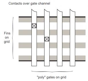
In the continuing evolution of Moore’s Law, the device structure and device/metal pitch lithography get the lion’s share of attention. The lowly contact typically gets little notice, despite its key impact on cell layout efficiency. In the advanced technology offering roadmap, Samsung Foundry emphasized contact litho and process enhancements as an enabler for increased density – look for “contact over gate channel” design styles to emerge.

(8) diffusion breaks and stressors
Another emerging cell layout topology is to reduce the distinct “diffusion breaks” between cells.
The isolating dummy gates provide lithographic uniformity. In the advanced technology presentation, Samsung Foundry also highlighted the ongoing focus on “stressor engineering” associated with the dummy gates, to improve carrier mobility and device performance.
(7) security IP
One of the best quotes of the day came from Hong Hao, SVP Marketing, in a presentation entitled “Enabling the Connected World” – “There is no safety without security.”
Samsung Foundry has invested in a suite of security IP offerings, in support of the “EVITA” security standards for automotive subsystems, for the fully-networked automobile: http://www.evita-project.org/

In addition to the ISO26262 and AEC-Q100 design verification and qualification requirements, the EVITA standard will also emerge as a lingua franca for automotive engineers.
A comparable IP security platform for IoT applications will be available from Samsung Foundry in 2018 – e.g., secure processing unit, crypto unit, root-of-trust unit.
(6) FD-SOI technology enhancements
Samsung Foundry has focused on their FD-SOI technology roadmap. The 28FDS node has been in high volume manufacturing for some time. “There are 17 products currently in HVM.”, according to SD Kwon, SVP, Logic Process Architecture.
Two significant enhancements to 28FDS were presented:
a) the characterization/qualification of RF device models, in anticipation of 5G mmWave communications adoption
- f[SUB]max[/SUB] > 400GHz, 110GHz device characterization, RVT/LVT devices
- customer product tapeout in 2018
b) an embedded MRAM offering by YE’18
- qualification testing underway: HTS, HTOL
- retention testing (115 degrees, 1KHrs)
- endurance testing (105 degrees, 1M cycles)
Also, a follow-on to 28FDS was introduced – 18FDS.
The 18FDS v0.1 PDK will be available in September, 2018, the v1.0 PDK on 5/19, and the v1.2 PDK on 12/19 (with eMRAM support). The operating voltage will be reduced from 1.0 V for 28FDS to 0.8V for 18FDS.
The 18FDS node will offer +22% performance or -37% power, and -35% area compared to 28FDS. An ultra-low leakage to ultra-low Vt device selection will be available. As with 28FDS, RF device characterization and eMRAM support will be available. This node leverages the existing BEOL lithography and process modules from the (mature) 14nm FinFET node.
(5) AiP
Also in support of the anticipated demand for 5G mmWave products, the Samsung Foundry presentation on advanced packaging highlighted the “Antenna-in-Package” offerings that will be available.
(4) advanced technology roadmap
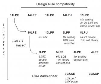
Samsung Foundry presented a two-dimensional roadmap – see the figure below.

One axis denotes design rule compatibility with PPA gains achieved through cell design and (incremental) device and litho updates. Customers seeking specific power, performance, or area gains will have additional technology options. The number of nFET/pFET fins in the cell height may be reduced in the cell library, to achieve greater density in successive nodes. A ULVT device is introduced for some nodes.
The other axis is the innovation progression, with generational litho and device engineering enhancements (more on that shortly).
Another technology option that Samsung Foundry is pursuing is the qualification of a “near Vt” cell library. The operating voltages will be 0.4V for 14LPC and 0.35V for 10LPP.
(A personal comment – I’m not sure the comprehensive methodology for parasitic extraction and reduction, delay calculation, noise analysis, and noise impact on delay methodologies for near Vt operation are quite ready yet… definitely worth more investigation.)
(3) FO-PLP packaging
FanOut-Wafer-Level technology (FO-WLP) has been a boon to designers seeking to implement high pin-count chips and/or to integrate multiple die in a low-cost, small-footprint package. A wafer carrier is used for attachment of good die (face-down), which are then encapsulated in a backside molding compound. After the carrier is separated, the replacement wafer of die and molding compound is presented for further processing.
Samsung Foundry has adapted this technology, to provide a significant throughput/cost enhancement. “We recognized that the wafer-level substrate for FO-WLP is inefficient around the wafer circumference. We have modified the process flow to introduce a panel substrate, an offering we call FO-PLP.”, explained Dae-Woo Kim, VP Packaging Development.

Innovation often arises from reviewing the most fundamental concepts. FO-PLP mass production has started.
(2) 7LPP and EUV
If you have been following the semiwiki articles on the progress of EUV, you are likely aware that Samsung Foundry decided to go “all in” on the deployment of EUV lithography for the 7nm node. The highlights of the 7LPP node are:
- manufacturing throughput: 1300 WPD in 2019, with a 250W EUV source (sustained)
- -46% area, +17% perf. / -48% power compared to 10FF
- two SC libraries available: 7.5T (3 nFET / 3 pFET fins) and 6.75T (2 / 2)
There were some very interesting comments relative to 7LPP that I thought were of specific note.
“The design complexity is reduced with the 7LPP design rules… it’s like going back to the future… it is as easy to use as 28nm.” (IP designer)
“The accuracy of our OPC (predictive) modeling is far improved… we are seeing far fewer litho hot spots.” (Samsung Foundry)
I hadn’t given much thought to the relative difficulty of mask data generation and optimization for the (broad deployment) EUV process. I found it interesting that lithography simulation accuracy is significantly improved.
(1) 3GAAE
The biggest news of the forum (IMHO) was the very aggressive schedule provided for the introduction of the 3nm gate-all-around nanosheet-based technology offering.
“We are pulling in the 3nm node introduction. The initial PDK will be available next year.”, E.S. indicated.
The (preliminary) specifications for 3GAAE are:
- 1.2X performance over 7LPP
- 0.5X power from 7LPP
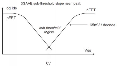
The unique nature of the gate-channel electrostatics of the gate-all-around structure offer near-perfect sub-threshold characteristics.

“We are looking forward to the design flexibility of stacked nanosheet devices, transitioning away from the quantized device width of the FinFET era.” (IP designer)
Miscellaneous
There were some other quotes of note:
“I originally thought that FD-SOI was going to be a one-node solution… Samsung Foundry is clearly crafting this technology toward the market.” (EDA provider)
“The decision to pursue EUV for 7LPP was a bold move. With the roadmap presented today – especially for 3GAAE – Samsung Foundry is continuing to be aggressive.” (EDA provider)
“We will be providing the required IP in the appropriate technology for emerging application markets, from the high-performance requirements of 112Gbps networking and GDDR6 memory bandwidth to the ultra-low leakage devices for power-sensitive products. And, we will continue to focus on security-compliant IP offerings.” (Samsung Foundry)
Is Moore’s Law done? Not yet.
For more information on Samsung Foundry, please visit the following link:
https://www.samsungfoundry.com/foundry/homepage.do
-chipguy
Share this post via:


Is Intel About to Take Flight?