
As EUV lithography is being targeted towards pitches of 30 nm or less, fundamental differences from conventional DUV lithography become more and more obvious. A big difference is in the mask use. Unlike other photolithography masks, EUV masks are absorber patterns on a reflective multilayer rather than a transparent substrate.… Read More

Author: Fred Chen
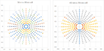
Pattern Shifts Induced by Dipole-Illuminated EUV Masks

Revisiting EUV Lithography: Post-Blur Stochastic Distributions
In previous articles, I had looked at EUV stochastic behavior [1-2], primarily in terms of the low photon density resulting in shot noise, described by the Poisson distribution [3]. The role of blur to help combat the randomness of EUV photon absorption and secondary electron generation and migration was also recently considered… Read More
The Challenge of Working with EUV Doses
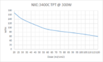
Recently, a patent application from TSMC [1] revealed target EUV doses used in the range of 30-45 mJ/cm2. However, it was also acknowledged in the same application that such doses were too low to prevent defects and roughness. Recent studies [2,3] have shown that by considering photon density along with blur, the associated shot… Read More
Blur, not Wavelength, Determines Resolution at Advanced Nodes
Lithography has been the driving force for shrinking feature sizes for decades, and the most easily identified factor behind this trend is the reduction of wavelength. G-line (436 nm wavelength) was used for 0.5 um in the late 1980s [1], and I-line (365 nm wavelength) was used down to 0.3 um in the 1990s [2]. Then began the era of deep-ultraviolet… Read More
Cautions In Using High-NA EUV

High-NA EUV has received a lot of attention ever since Intel put the spotlight on its receiving the first 0.55 NA EUV tool from ASML [1], expected in 2025. EUV itself has numerous issues which have been enumerated by myself and others, most notoriously the stochastic defects issue. There are also a host of issues related to the propagation… Read More
Stochastic Effects from Photon Distribution Entropy in High-k1 EUV Lithography
Recent advances in EUV lithography have largely focused on “low-k1” imaging, i.e., features with pitches less than the wavelength divided by the numerical aperture (k1<0.5). With a nominal wavelength of 13.5 nm and a numerical aperture of 0.33, this means sub-40 nm pitches. It is naturally expected that larger… Read More
Stochastic Origins of EUV Feature Edge Roughness
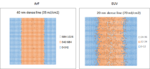
Due to the higher energy of EUV (13.3-13.7 nm wavelength) compared to ArF (193 nm wavelength) light, images produced by EUV are more susceptible to photon shot noise.
Figure 1. (Left) 40 nm dense (half-pitch) line image projected onto wafer at 35 mJ/cm2; (Right) 20 nm dense (half-pitch) line image projected onto wafer at 70 mJ/cm2.… Read More
Contrast Reduction vs. Photon Noise in EUV Lithography
The stochastic behavior of images formed in EUV lithography has already been highlighted by a number of authors [1-3]. How serious it appears depends on the pixel size with which the photons are bunched. Generally, though, for features of around 20 nm or less, even 1 nm can have at least a +/- 15% gradient across it, which is still a
SALELE Double Patterning for 7nm and 5nm Nodes

In this article, we will explore the use of self-aligned litho-etch-litho-etch (SALELE) double patterning for BEOL metal layers in the 7nm node (40 nm minimum metal pitch [1]) with DUV, and 5nm node (28 nm minimum metal pitch [2]) with EUV. First, we mention the evidence that this technique is being used; Xilinx [3] disclosed the… Read More
Calculating the Maximum Density and Equivalent 2D Design Rule of 3D NAND Flash
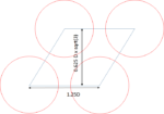
I recently posted an insightful article [1] published in 2013 on the cost of 3D NAND Flash by Dr. Andrew Walker, which has since received over 10,000 views on LinkedIn. The highlight was the plot of cost vs. the number of layers showing a minimum cost for some layer number, dependent on the etch sidewall angle. In this article, the same… Read More


Intel: Pushing EMIB Forward: Design Methodology Insights with Synopsys Tools