You are currently viewing SemiWiki as a guest which gives you limited access to the site. To view blog comments and experience other SemiWiki features you must be a registered member. Registration is fast, simple, and absolutely free so please,
join our community today!
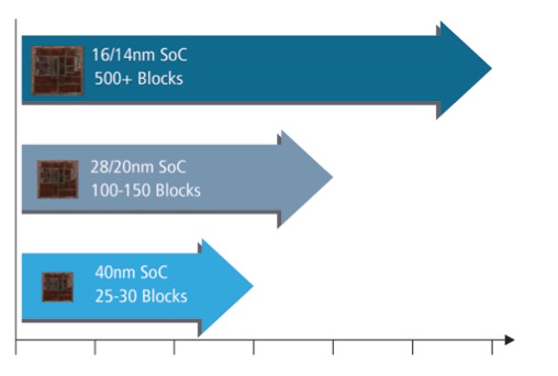
Combine the pressures of Moore’s Law which enable billion transistor SoCs and the shortened time to market from consumer electronics product cycles and you have the perfect storm for EDA tool vendors. A modern SoC can have 500 or more blocks, creating both a design and verification challenge. How in the world do you write … Read More
The attraction to an IP-based design methodology is that you can assemble an SoC from ready-made IP blocks, saving you valuable engineering development and verification time, while reducing risks from having to develop something from scratch and hoping that they meet industry standard specs. ARM is well known for supplying … Read More
The personal computing market started out back in the late 1970’s, with IBM being a relative late-comer in 1981, however over many decades we’ve seen the unit volumes steadily increasing each year driving demand of semiconductors of all types. IC Insights is a research company that follows the personal computer … Read More
Since 1978 I’ve seen many trends in the semiconductor design world: transistor-level IC design, gate-level design, RTL coding, High Level Synthesis (HLS) and IP re-use. We’ve witnessed the growth in design productivity enabling chips starting with just thousands of transistor all the way up to billions of transistors… Read More
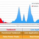
On your last SoC project how well did your dynamic power estimates match up with silicon results, especially while running real applications on your electronic product? If your answer was, “Well, not too good”, then keep reading this blog. A classical approach to dynamic power analysis is to run your functional testbench… Read More
For SoC designers attending DAC in June you probably want to check out the EDA vendors that enable design collaboration among your engineers and designers that are spread out across a building, campus or the globe. Dassault Systemes does offer tools and methodologies for: Design collaboration, requirements and IP management.… Read More
Every SoC project that I know of wants to finish on time, under budget, and maximize profits per device. When I first started out doing DRAM design I learned that we could maximize profit by doing shrinks of existing designs, move from ceramic to plastic packages, and reduce the amount of time spent on a tester. Today, the economic … Read More
My typical DACtrip is a blur of non-stop interviews with EDA, IP and Semiconductor vendors followed by a few dozen blogs to share what I’ve learned. I just became aware of something a bit different at DAC this year by talking with Jill Jacobs, an organizer for an event dubbed Heart of Technology (HoT) where they raise money for… Read More
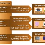
We live in very interesting times, you can wear an Android watch from Samsung that uses 14 nm FinFET technology, attend the 52nd DAC conference in June to learn about EDA and IP vendors supporting FinFET, and read about research work for new devices down to 5 nm. TCAD is that critical software technology that enables the development… Read More
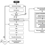
Digital IC design has been largely automated with high-level languages, RTL coding, logic synthesis, and automated place and route tools. What about analog IC layout automation, is it possible? A few EDA companies think that it is possible and even practical. In recent memory there were two companies really focused on analog … Read More


Consolidation and Competition: Who is Winning the $4.5 Billion Interface IP Race?