You are currently viewing SemiWiki as a guest which gives you limited access to the site. To view blog comments and experience other SemiWiki features you must be a registered member. Registration is fast, simple, and absolutely free so please,
join our community today!
Semiconductors continue to surge and lead technology sectors all over the world. TSMC has always been my economic bellwether and 2019 was another great year as the TSM share price almost doubled. But it looks like the best is yet to come with TSMC significantly increasing CAPEX to cover 7nm and 5nm demand.
TSMC CEO C.C. Wei increased… Read More
Over the last 40 years, Bernard has worked with semiconductor and EDA companies in hands-on, management and consulting roles in engineering, sales and marketing. He most recently co-founded Atrenta where he created and led the development of SpyGlass, retiring as CTO when Atrenta was acquired by Synopsys. Post-retirement,… Read More
The media is trying to disparage the semiconductor industry again. It’s hard to not take this type of desperate journalism personal. Semiconductor people are the smartest and hardest working people in the world and we deserve better, absolutely.
TSMC founder sees trade dispute as ‘reality show with no script’… Read More
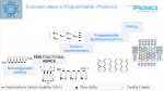
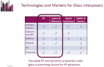
I recently wrote about this year’s Cadence Photonics Summit. As I mentioned in that post, it was a fascinating event with several companies providing useful and informative presentations. You can access some of the presentations on the event site. One presentation, given by Jose Capmany of iPronics, was especially interesting… Read More
I would guess that most people have seen or at least heard of the Matrix movies but how many people can remember who vanquished the earth to begin the series? It was artificial intelligence (AI) of course which seemed pretty far fetched 20 years ago, but today not so much. In fact, for those of us in the AI know it seems quite likely in some… Read More
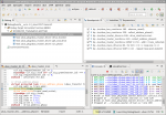
Every few months, I touch base with Cristian Amitroaie, CEO of AMIQ EDA, to learn more about how AMIQ is helping hardware design and verification engineers be more productive. Quite often, his answers surprise me. When he started describing their Design and Verification Tools (DVT) Eclipse Integrated Development Environment… Read More
On November 13, Cadence held its annual Photonics Summit. Cadence has been hosting this event for several years with the intention of advancing the photonics industry. With this event, Cadence has been a catalyst in furthering photonic product development. It’s quite remarkable that Cadence hosts such an event in a field where… Read More
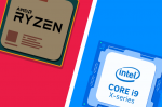
The Intel versus AMD rivalry is legendary amongst us Silicon Valley AARP members and is one of the reasons why the semiconductor industry is as competitive as it is today, absolutely.
AMD’s boisterous corporate culture started with AMD’s co-founder and long time CEO Jerry Sanders. Jerry was the ultimate showman but his credo “People… Read More
One of the many benefits of blogging for SemiWiki is the free conference passes and buffet lunches, absolutely. IEDM is one of the more prestigious semiconductor conferences, now in its 65th year, is being held at the Hilton Hotel in San Francisco’s famed Union Square this week. This year more than 1,910 semiconductor professionals… Read More
Bob Swan is really starting to grow on me. Admittedly, I am generally not a fan of CFOs taking CEO roles at semiconductor companies but thus far Bob is doing a great job. This comes from my outside-looking-in observations and from the people I know inside Intel, absolutely.
Bob did a fireside chat with Credit Suisse at their 23rd annual… Read More


Captain America: Can Elon Musk Save America’s Chip Manufacturing Industry?