You are currently viewing SemiWiki as a guest which gives you limited access to the site. To view blog comments and experience other SemiWiki features you must be a registered member. Registration is fast, simple, and absolutely free so please,
join our community today!
SEMI Forecasts 15% Increase in Fab Equipment Spending for 2015
With worldwide capex growth of 8%, fab equipment spending is expected to increase by 15% in 2015, according to the most recent edition of the SEMI (www.semi.org) World Fab Forecast. SEMI’s data also predicts a slowdown of fab equipment spending in 2016 to low single … Read More
As a reminder, the Synopsys v. Mentor drama started when Synopsys filed a Complaint for Declaratory and Injunctive Relief on the same day (September 27, 2012) as they entered into an agreement to acquire emulation provider EVE (ZeBu emulator systems), which competes with Mentor’s Veloce family of emulators. Apparently, upon… Read More
The long running legal action between the top two NVM IP companies is now finished after close to five years of lawyering. By the way, I write about this stuff in hopes of limiting the future earning power of lawyers that prey on our R&D budgets. This one is significant because Kilopass was not successful in a patent infringement… Read More
TSMC ♥ UMC?by Daniel Nenni on 03-18-2015 at 8:00 pmCategories: Semiconductor, TSMC
The relationship between TSMC and UMC is one of the more interesting ones in the fabless semiconductor ecosystem in my opinion. Both are headquartered in Hsinchu Taiwan and it is very hard to visit one company without seeing the other as they have facilities right across the street from each other. They also share humble beginnings… Read More
Take a look at the figure below and tell me this information did not come from inside Apple. The question is: Was it voluntary or involuntary? Inquiring minds want to know! There are some minor surprises which I will get to in a minute but the actual source information is spot on to what I have heard the past few quarters. This spicy little… Read More
In the traditional sense “Shift Left” is the process of making things simpler in an effort to make things faster. Shift Left was the theme of theDVCon keynote last week delivered by Synopsys co-founder and co-CEO Aart de Geus which is right on topic when it comes to modern semiconductor design and manufacturing, absolutely.
KEYNOTE:… Read More
In preparation for this blog I Googled around to get the latest information made available by Altera to see if it matches up with what I know from discussions amongst the fabless semiconductor ecosystem companies. Unfortunately when I Googled Altera+20nm+14nm the first three entries from the Altera website were Error 404 Page… Read More
You have to love when a professional journalist leaks a story and cites a “source close to the acquisition.” News flash: Anyone “close” to the acquisition is under NDA which is a legally binding agreement, not very professional if you ask me. Bloggers however can write whatever they want but since I was actually “close” to … Read More
Apparently that is the case. Honestly my choice would have been Mentor but I can easily make an argument for Cadence based on my discussions with the foundries and their top customers but more on that later.
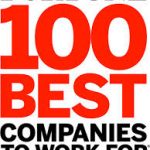
Fortune Magazine last week added Cadence to the 2015 list of “100 Best Companies to Work For” citing a cultural transformation… Read More
As big of a fan as I am of Social Media there is still nothing like getting up close and personal when collaborating with the fabless semiconductor ecosystem. After 30+ years in Silicon Valley if there is one thing I have learned it’s that “showing up” is the #1 key to success, absolutely.
Speaking of showing up, each year there are three… Read More


Enhancing Multi-Domain System Simulation with FMI Co-Simulation