The increasing demand for data communication throughput between system components has driven the requirement for faster SerDes IP data rates. The complexity of the transmit (Tx) and receive (Rx) signal conditioning functions has correspondingly evolved. As a result, the simulation methodology for SerDes electrical interface verification needs to encompass the entire signal path, while maintaining simulation efficiency. To best address system modeling requirements with the wide diversity of SerDes implementations, the electronics industry adopted a new modeling approach – the I/O Buffer Information Specification-Algorithmic Modeling Interface (IBIS-AMI) – as maintained by the IBIS Open Forum consortium (link).
Background
A serial lane is used to transmit data over a differential wire pair, where the system physical backplane (or other PCB motherboard + daughter card topology) represents a significant electrical “distance”. Multiple lanes are commonly integrated into a “link” – e.g., a SerDes IP block may provide a data communications link comprised of 8 lanes.
Each data bit in the serial stream is denoted in the time domain as a unit interval (UI) – the electrical topology of the lane between components will incorporate many UI’s. For example, at very high data rates, a UI could be comparable in physical dimension to a through-board signal via. As a result, to maintain a suitably low bit error rate (BER), the accuracy of model extraction and simulation is paramount.
As illustrated below, there will be significant frequency-dependent insertion loss attenuation (IL) in the transmitted signal through the board trace materials and stack-up (e.g., FR-4, Megtron).
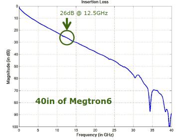
Figure 1. Example of insertion loss versus frequency.
The signal will also be subjected to reflection loss (RL) from impedance mismatches, which thus also impact IL. Additionally, near-end and far-end crosstalk losses (NEXT, FEXT) from neighboring switching activity also degrade the signal. As the (effective) clock for the series data is embedded in the signal transitions, any jitter in the time reference for each UI further complicates the clock-data recovery (CDR) at the Rx end.
Early SerDes electrical analysis used a simplified IBIS electrical model of the Tx driver and Rx receiver, merged with the extracted (S-parameter based) loss model of the SerDes lane. SerDes architects were then responsible for merging this analysis with the equalization functionality in the Tx and Rx blocks.

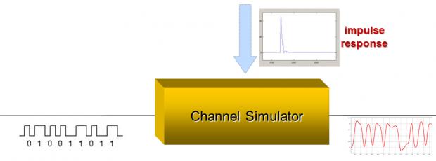
Figure 2. Example of a Tx driver and Rx receiver IBIS model merged with the serial lane; the channel response characteristics are derived from the impulse response.
The introduction of the IBIS-AMI specification enabled architects to develop a comprehensive simulation model. EDA companies extended their signal integrity simulation tools in support of this additional model capability. Yet, the adoption of IBIS-AMI models by SerDes IP developers to release to SoC customers was progressing slowly.
IBIS-AMI Model Generation
I had the opportunity to chat with Ken Willis, Product Engineering Architect at Cadence about the IBIS-AMI modeling features, and the novel developments at Cadence to help accelerate the adoption rate.
Ken began,“Since the introduction of PCIe (@ 2.5Gbps), designers have understood the critical requirement for full channel simulation of serial links, including equalization models. The Algorithmic Modeling Interface definition was added to the basic IBIS specification. However, IBIS-AMI model generation requires a unique skill set – part SerDes architect, part signal integrity engineer, part software developer. This need for this diverse expertise impeded the adoption of IBIS-AMI by IP developers. The Sigrity System SI team at Cadence recognized this issue, and released the AMI Builder.” (video link).
Ken continued, “AMI Builder provides a wizard-based flow. SerDes designers utilize a library of algorithms to define their architecture. These algorithmic building blocks have been developed in close collaboration with the Cadence internal IP team. Each wizard includes a broad set of implementation options and parameters for the SerDes IP designer to select. The generated IBIS-AMI model is directly compilable into the Sigrity SI simulation platform.”
For example, consider the signal conditioning typically incorporated into the Tx side of the SerDes lane. A data value transition includes a significant spectral energy at high frequencies. Due to the IL characteristics of the signal trace, this energy is severely attenuated – to compensate, an “emphasis” is applied to the transition edge. Also, there will be remaining signal energy at the Rx after the UI time interval – a phenomenon denoted as “inter-symbol interference” (ISI). To reduce this energy, both “pre-cursor” and “post-cursor” signal energy derived from adjacent data values may be incorporated into the Tx waveform provided to the driver.
A feed-forward equalizer (FFE) SerDes block is typically included in the architecture, with weighted “taps” representing the contribution of successive cursors, which ultimately add/subtract to the driver current.

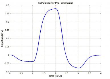
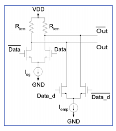
Figure 3. FFE signal emphasis at the Tx end of the SerDes. The top figures illustrate the data waveform from the FFE. The schematic in the bottom figure illustrates a simple emphasis circuit with the current and delayed data input “taps” — the “delayed” data also influences the signal current at the differential outputs.
The AMI Builder library includes a Tx FFE algorithm, with a wizard to assist with defining the options for the cursor tap configuration and tap coefficients.
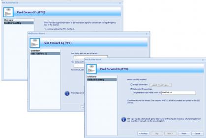
Figure 4. The AMI Builder FFE wizard options.
A general SerDes architecture typically includes several blocks, as illustrated below.
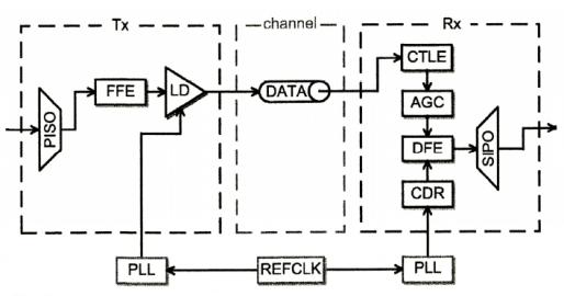
Figure 5. SerDes architecture example (PISO: parallel-in, serial-out; SIPO: serial-in, parallel out)
The signal conditioning at the Rx typically includes:
- agc (automatic gain control): amplifies the signal magnitude after Tx equalization and trace losses
- ctle (continuous-time linear equalizer): an example of an analog CTLE filter is shown below, both passive and active; digital CTLE implementations are also common
- cdr (clock data recovery): using the time reference at the Rx, the clock phase is adjusted to the optimal capture point in the data UI time window
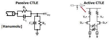
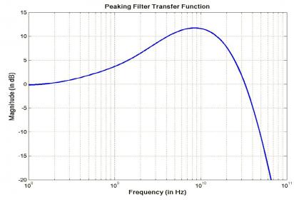
Figure 6. Examples of simple analog CTLE filters; a typical active filter response curve is shown.
The common eye diagram depicts equalized (superimposed) data waveforms, illustrating magnitude and phase (jitter) variations. The CDR aligns the capturing clock edge at the horizontal center of the eye; the vertical maximum of the eye is compared to the (differential) voltage margin associated with the Rx clocked “slicer” circuit that stores the incoming data value.
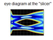
Figure 7. Eye diagram after Rx signal equalization
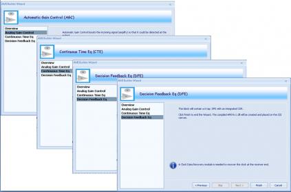
Figure 8. Illustration of the AMI Builder wizards for Rx blocks
Ken highlighted, “The IBIS-AMI spec supports a variety of representations of SerDes blocks. As an example, for the CTLE filter, designers could provide a text file with: the pole-zero rational functions in s-parameter format, a mag/frequency description, or the step function response. AMI Builder will synthesize and plot the filter response.”
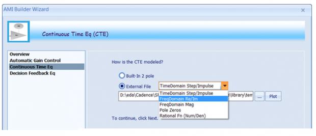
Figure 8. AMI Builder CTLE wizard
Ken continued, “Architects have the flexibility to construct the AMI Builder model to fit their specific configuration. For example, the positioning of the CTLE could be swapped with the AGC. If there is a need for a user-defined block model not present in the library, designers can provide their own C-code – say, for an AGC with unique compression or magnitude clipping characteristics.”
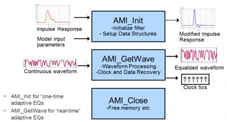
Figure 9. IBIS-AMI model interface API’s
I asked Ken, “Once a SerDes IP developer has solidified their internal implementation with AMI Builder, how is the IBIS-AMI model released to the end customer?”
Ken replied, “The IP developer defines which parameters in the IBIS-AMI model are reserved and which are editable. For example, end user-defined parameters could range from SerDes IP configuration specifics to the overall system jitter impairment.”
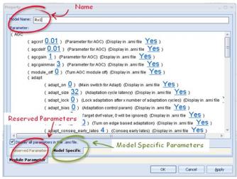
Figure 10. Illustration of reserved and user-defined parameters in the IBIS-AMI model
“What’s ahead for IBIS-AMI and the AMI Builder?”, I inquired.
Ken replied, “The first wave of IBIS-AMI users are SerDes IP developers and customers. The advent of very high-speed DDRx parallel interfaces also requires signal equalization, and thus comparable approaches. The modeling of the parallel interface clock strobe compared to serial clock recovery requires attention, to accurately represent the analog strobe waveform as the timing reference.”
(For example, see the follow DesignCon 2018 paper on DDR5 AMI model generation, describing the collaboration between Micron Technology and Cadence – link.)
“Also, the evolution of a SerDes lane to a pulse-amplitude modulation waveform for multiple-level encoding will require AMI modeling focus – for PAM-4, equalization models need to correct 4 signal levels.”, Ken added.
IBIS-AMI models are now de rigueur for SerDes IP system integration. SerDes designers need to incorporate this model (and the related configuration documentation) into their IP customer enablement deliverables. Yet, the expertise needed to prepare and verify this complex model requires diverse skills – kudos to Cadence for providing the automation aids to expedite development of IBIS-AMI models.
-chipguy
Share this post via:


Comments
There are no comments yet.
You must register or log in to view/post comments.