 It is no secret that custom ICs are getting larger and more complex and this has driven chip design teams to split up into smaller teams to handle the manual or semi-automated routing of the many blocks and hierarchical layers that go to make up such a design. These sub-teams don’t just need to handle the routing within their own block(s) but also integrate the routing between the blocks and also address the challenge of creating correct top-level routing (that overflies the block) within the assigned part of the die.
Using informal approaches, such as verbal and email status reports, is no longer enough and makes the routing of a large custom chip become the long pole in the tent, very labor-intensive and with a schedule that determines the overall schedule of the entire chip. Once you add in congestion issues, advanced-node parasitic effects, the fact that the design itself is probably not stable and undergoing incremental change, then the process becomes almost impossible. Even “industry standard” routers are unable to complete top level routing challenges because they were not designed to fully address the complex combination of specialized topologies, hierarchical design rules and DFM requirements (via redundancy, via orientation, via enclosures, wire spreading, etc) that are required to achieve successful on-time design closure for AMS and custom ICs.
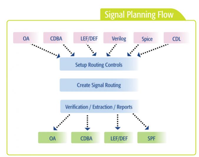
 What is needed is a fully automated approach to signal planning. The key is to integrate the process with the block placement tasks and the use of intelligent, routing aware pin-placement algorithms to address multi-topology routing problems. Providing a tool with tight integration of these tasks means that designers can explore the implications of different placement alternatives before deciding on an optimal solution. And in a much faster time than doing it manually or semi-automatically.
One critical consideration is the routing style required to handle these complex top-level and block routing tasks. A manhattan routing style is used to avoid jogs, thus reducing the number of vias required and minimizing wire length, in turn reducing timing delays and power. Nets can be sorted during routing to avoid crossing routes, thus reducing crosstalk and other noise. Of course users must be able to define constraints for the router, such as width, shielding requirements, maximum and minimum widths on each layer and identifying matched signal pairs.
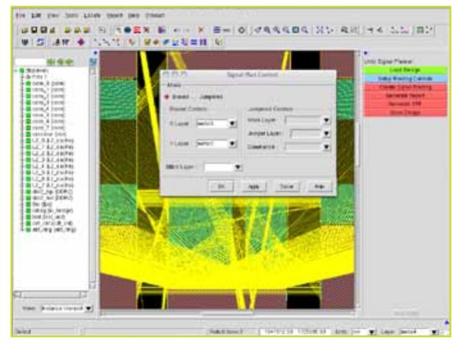
Another way to optimize area and improve productivity is to use a router which supports multiple-bias routing as well as strictly biased X-Y routing. With its jumpered-mode designers can define complex schemes where all routes in both horizontal and vertical biases can use the same metal layer efficiently, allowing a separate layer to be used as a jumper layer for channels where a layer change is required to route effectively. Further, many semiconductor manufacturers use routers that support special optimization for bus routing and compact signal routing, allowing them to take advantage of specialized semiconductor vias and via directions resulting in still more compact routing.
More information on PulsIC’s Unity Signal Planner is here.
Note: You must be logged in to read/write comments
Share this post via:


The Intel Common Platform Foundry Alliance