





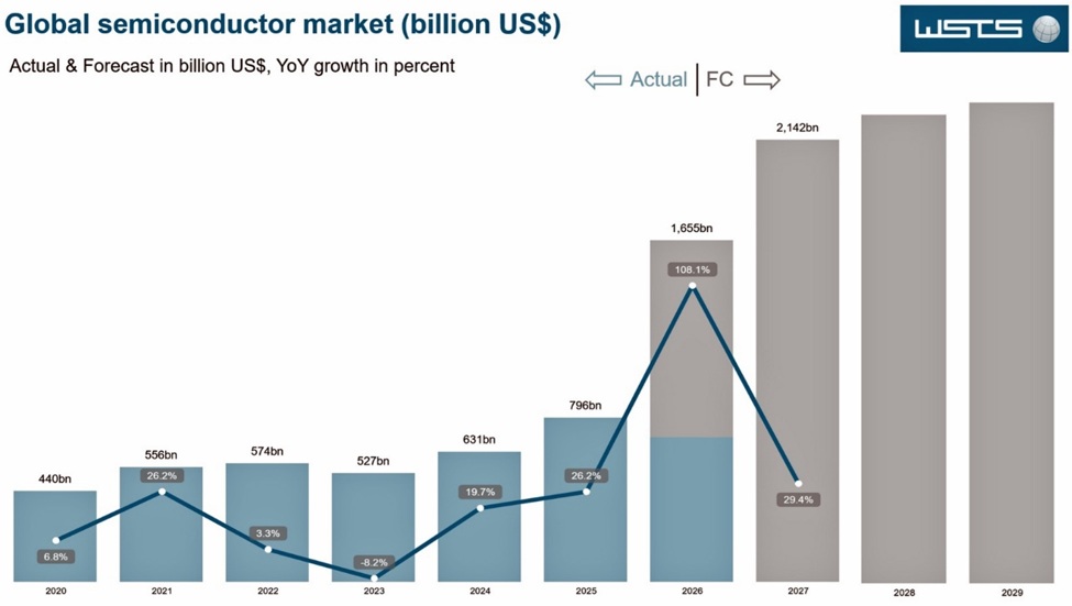
Champagne is an unusual opening act for a semiconductor conference. At SEMICON West 2026, October 13 to 15, at the Moscone Center in San Francisco, it served a purpose. The toast marked an industry that has already crossed $1 trillion in annual revenue, almost four years ahead of earlier projections.
WSTS (World Semiconductor Trade Statistics) put first-half 2026 sales at $702 billion, double a year earlier, and its August update points to roughly $1.66 trillion for the full year, with memory up about 300%. SEMI chose its theme to match: the road from one trillion to two.
By the numbers
SEMI expected more than 35,000 attendees over the three days on a sold-out floor of over 1,500 booths. Final attendance had not been released when this was written. By SEMI’s own figure, the exhibitor count is more than 700 companies and organizations, covering the whole microelectronic supply chain, from EDA and IP, fabless designers and the big IDMs to equipment and materials.
Four topics ran through almost every room: AI scaling, heterogeneous integration, advanced manufacturing and supply-chain resilience. Behind them sat an enviable problem. Demand is extraordinary; the hard part is meeting it within the limits of power, cost and production readiness.
The CEO Summit stage
Each morning (8:30 to 11) ran under its own banner: “Semiconductors Today” on Tuesday, “Transform Tomorrow” on Wednesday and “Meeting the Industry’s Needs” on Thursday.
The session I had circled was Sassine Ghazi’s fireside chat with Ed Sperling of Semiconductor Engineering. The Synopsys CEO described how the company has embedded agentic AI across its entire, very large product portfolio. Few EDA leaders have been this explicit about where the design flow is going. It also raised a question well beyond EDA: what happens when AI takes a growing role in designing the hardware it runs on? Speed is the easy part to demonstrate. Proving that the silicon comes out right is harder.
Other sessions worth the early start:
- Lalitha Immaneni (VP, Semiconductor R&D, Intel Foundry) on the system era and scaling AI through heterogeneous integration.
- Scott Gatzemeier (Corporate VP, Front End US Expansion, Micron) and Kevin Younis (COO, Empire State Development) on the partnership behind large domestic fab projects.
- Bill Frauenhofer (Executive Director, Semiconductor Investment and Innovation, U.S. Department of Commerce) and David Reeder (CEO, Entegris) on policy and the U.S. supply chain.
- Timothy Costa (VP and GM, Industrial and Computational Engineering, NVIDIA), David Jarzynka (CEO, Brooks Automation) and Thomas Sonderman (CEO, SkyWater Technology).
- Public-sector voices, including Brian Stone of the National Science Foundation and the mayors of San Francisco, San Jose and Phoenix. Kate Gallego’s presence was fitting: Phoenix takes over the show next year.
Two afternoon panels filled the same stage: a Geopolitical Summit on Tuesday, and on Wednesday “From Fragile to Future-Ready: AI-Powered Resilience for the $2T Semiconductor Supply Chain.”
A day for design
Tuesday also brought something SEMICON West long lacked: a full day on design. “Bridging Design and Manufacturing with AI,” organized by the ESD Alliance, a SEMI Technology Coalition, and chaired by Ming Zhang of PDF Solutions, ran 10 talks and one panel with standing-room only at many sessions. Yatin Trivedi, Head of Semiconductor Center of Excellence (CoE) at Capgemini Engineering, served as afternoon moderator and organizer of the lunch panel.
TSMC’s L.C. Lu opened with “Scaling Leadership Silicon with AI.” Applied Materials, Cadence, Cerebras, Intel Foundry, Lam Research, PDF Solutions and VerifAIX followed. The range was wide: wafer-scale computing redesigned for hyperscale AI, AI-enabled system-technology co-optimization (STCO) at advanced nodes, secure data platforms from front end to advanced packaging, IP in AI-based design, a trust layer for autonomous chip design, and agentic AI in the fab. McKinsey’s Aaron Aboagye closed with “Design at AI Speed,” on compressing time-to-silicon.
The day’s lesson: design now depends on packaging, process and fab data, and the fab needs earlier sight of what designers intend. AI can carry that exchange, but only with usable data, secure collaboration and trust in automated decisions.
Agentic AI: What It Costs, What It Returns
The economics of agentic AI received particular attention during an IEEE-hosted panel moderated by Silvaco CEO Wally Rhines. Featuring executives from Applied Materials, Cadence, Lam Research, Intel Foundry, and Sandisk, the discussion was framed around a simple question: What does agentic AI actually cost, and what does it return?
The question goes beyond the price of computing resources. Deploying autonomous AI agents in semiconductor design and manufacturing requires access to reliable data, integration with established engineering tools, and rigorous validation of results. The potential rewards, however, extend beyond engineering productivity. Faster design iterations, shorter verification cycles, improved manufacturing yield, and reduced time to silicon deliver significant economic benefits.
The real test of agentic AI will therefore be less about how many engineering tasks it can automate and more about whether it can demonstrably reduce development time and manufacturing costs without compromising correctness.
Same Industry, Different Clocks: AI Adoption in Design vs. Manufacturing
In a session titled “AI Discontinuities in Design and Manufacturing,” Rhines explained why chip design took up AI some four years before manufacturing did. The reason, he argued, is scale. Design already deals with a vast number of parameters and attributes, but manufacturing involves orders of magnitude more. Training foundation models on that much data would take hyperscale data centers, at enormous cost and with an energy bill to match. Agentic AI is changing the equation. By splitting the problem into narrow tasks, each handled by a smaller specialized model, it sidesteps the need for one giant model, and SEMICON West 2026 showed how quickly manufacturing is taking advantage of it.
Beyond the main stage
Advanced packaging was the other strong thread. The Advanced Packaging and Heterogeneous Integration Summit tied chiplets, 2.5D and 3D integration, high-bandwidth memory and co-packaged optics to production realities: thermal density, inspection, yield and equipment readiness. For AI processors this is the crux. An architecture is only as good as the memory, interconnect and cooling that can be built and assembled at a sensible cost.
The smart manufacturing program covered digital twins, agentic and physical AI, and increasingly autonomous factories. Sustainability sessions dealt with energy, emissions, water and circularity; supply-chain sessions with visibility and resilience. Growth on the scale forecast needs all of it.
And there was beer. Tuesday evening’s Oktoberfest-style WestFest at Moscone South let conversations run on without a presentation clock.
PDF Solutions CONNECT 2026
On October 15–16, at the tail end of SEMICON West 2026, PDF Solutions held its 2026 CONNECT Conference at the Westin St. Francis in San Francisco. The two days were packed with keynotes and technical sessions, mostly from PDF Solutions specialists, with a few customer presentations adding real-world perspective.
My full report will follow shortly.
Conclusions
The trillion came early, and memory carried it. Nobody on stage was celebrating for long. The talk had already moved to two trillion and to whether fabs, power and people can keep up.
Design has finally earned a full day at a manufacturing show. AI is the reason: once the same models touch layout, process and yield, the wall between the two worlds starts to look expensive.
And the show is following the fabs. The next SEMICON West opens in Phoenix in March 2027. San Francisco got a good farewell.
Also Read:
Design the Right Chip: Why Prototyping Has to Be Easy
S2C Prodigy Complete Prototyping Solutions—and Why They Matter
Shift Left with S2C Prodigy: From RTL Verification to Real-World Software Validation
Share this post via:


ChipAgent Raises $134Million and Why it Matters