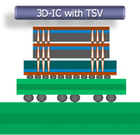
Two conferences on 3D, one just over and one coming up next week. The one that was just over was hosted by Georgia Tech, the 3rd Annual Global Interposer Technology Workshop (GIT). I wasn’t there but my ex-colleague from VLSI Technology Herb Reiter was. Herb has become very much associated with all things 3D since he led the working group created by GSA to coordinate their activities. He has written up his “trip report” over on the EETimes website. The big conclusion:”In a mega-panel moderated by Matt Nowak, a 3D stacking expert at Qualcomm, more than a dozen experts discussed a few technical and many business challenges related to interposers. They concluded the technology is ready but we need lower costs.”
I wrote earlier in the year about Xilinx and Micron who are using interposer and 3D designs. For now these are limited to very high priced devices that can absorb these costs. But if More than Moore is going to be an alternative to the huge number of process steps required for 10nm and 7nm (I’m assuming EUV won’t work well enough, but your opinion may vary) then it has to be economic not just for the highest price chips.
Herb’s overall conclusion:”This and similar data points during the workshop confirmed my fears that in many companies, management as well as system and IC designers still see interposer technology as a topic only for the packaging experts and of no or very limited impact on their own work or their company’s future. I believe risky projects and new technologies such as 3D chip stacking have to be sold to high-level management with their benefits to the business justified extensively.”
Coming up next week is the 10th Annual 3D Architectures for Semiconductor Integration and Packaging conference at the Hyatt Regency in Burlingame on December 11th to 13th. I will be going to that one and there will be blog(s) about it to enjoy with your holiday eggnog.
The opening keynote is by Doug Yu of TSMC’s integrated interconnect and packaging division on Wafer Scale System Integration Technology. As you may know, TSMC has a 3D technology they call CoWoS (Chip on Wafer on Substrate) which I assume will be one of the topics he will cover.
The second day keynote is by Kiavan Karimi of Freescale on Role of Advanced 3-D Packaging Architectures in Support of the Internet of Things (IoT) Edge/sensing Node devices. The IoT is for sure going to be cost-sensitive and so it will be interesting to see his opinion on whether we are on track to have costs coming into line.
Herb’s report is here. Details on 3D ASIP are here.
More articles by Paul McLellan…


The Intel Common Platform Foundry Alliance