Last night the IEEE Silicon Valley Chapter had a panel session that was in some ways a preview of some of what will be discussed at the Electronic Design Process Symposium in Monterey next Thursday and Friday. At EDPS Herb Reiter organized a session on FinFET, 3DIC and FD-SOI (sort of how many buzzwords can you get into one set of titles).… Read More

Tag: 2.5dic
3D: Atlanta and Burlingame
Two conferences on 3D, one just over and one coming up next week. The one that was just over was hosted by Georgia Tech, the 3rd Annual Global Interposer Technology Workshop (GIT). I wasn’t there but my ex-colleague from VLSI Technology Herb Reiter was. Herb has become very much associated with all things 3D since he led the … Read More
3D: the Backup Plan

With the uncertainties around timing of 450mm wafers, EUV (whether it works at all and when) and new transistor architectures it is unclear whether Moore’s law as we know it is going to continue, and in particular whether the cost per transistor is going to remain economically attractive especially for consumer markets … Read More
Dimensions of Electronic Design Seminars
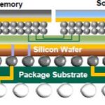
ANSYS and Apache are putting on a new series of seminars about designing future electronic systems. These are only getting more complex, of course, cramming more and more functionality into smaller portable devices with good battery life (and not getting too hot), integrating multiple antennas into a single platform, and TSV-based… Read More
3D Thermal Analysis
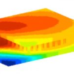
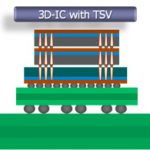
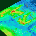
Matt Elmore of ANSYS/Apache has an interesting blog posting about thermal analysis in 3D integrated circuits. With both technical and economic challenges at process nodes as we push below 28nm, increasingly product groups are looking towards through-silicon-via (TSV) based approaches as a way of keeping Moore’s law… Read More
Cadence at Semicon West Next Week: 2.5D and 3D
Next week it is Semicon West in the Moscone Center from Tuesday to Thursday, July 10-12th. Cadence will be on a panel session during a session entitled The 2.5D and 3D packaging landscape for 2015 and beyond. This starts with 3 short keynotes:
- 1.10pm to 1.25pm: Dr John Xie of Altera on Interposer integration through chip on wafer on