Summary
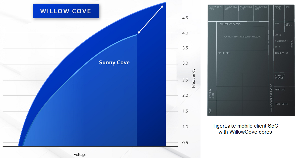
At the recent Intel Architecture Day 2020 symposium, a number of technology enhancements to the Intel 10nm process node were introduced. The cumulative effect of these enhancements would provide designs with a performance boost (at iso-power) approaching 20% – a significant intra-node enhancement, to be sure. The initial release of CPUs in this 10nm “SuperFin” process is scheduled for this Fall, as part of the 11th-Generation TigerLake mobile client product family announcement, based on the WillowCove core. (The Sapphire Rapids Xeon server processor on an enhanced SuperFin process will ship in 2H21.)

Figure 1. Performance boost for the WillowCove core, and a TigerLake SoC block diagram.
Background
CPI for Yield
After a process technology reaches production volume qualification status (“v1.0”), fabrication engineers remain focused on continuous process improvement (CPI). These ongoing improvements span a wide range of areas, from additional materials quality inspections to photolithography exposure window optimizations to (deposition and/or etch) equipment updates. Collectively, these new manufacturing steps fall under the broad heading of statistical process control (SPC). The goal of this CPI effort is to improve fabrication yield, from both defect density reductions and reducing the (3-sigma) performance variation endpoints.
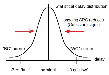
Figure 2. Illustration of the overall (Gaussian) performance distribution, and the common “3-sigma” WC/BC design targets.
The transition to a new CPI-driven process variant is typically done with the encouragement of the foundry’s customers, as yield is improved, although some customers may wish to review the engineering updates with the foundry to assess any product re-qualification requirements. A key characteristic of this CPI effort is that no (major) lithography design rule modifications are introduced – only an assessment of the need for re-analysis of electrical characteristics and/or post-silicon re-qualification.
A Process Node “Kicker”
There is another class of CPI-based enhancements, commonly known as a mid-life kicker. After customer parts are shipping in volume, a more significant set of process enhancements may be available, potentially including lithography design rule updates. A long-life, high-volume product might be a candidate for the engineering investment to re-target an existing design to the new process variant, to offer a product mid-life “kick” to the performance specifications.
In the era of Dennard scaling for CMOS technology, these mid-life process variants were commonly associated with the introduction of a half-node, typically a broadly-applied 90% “shrink” of the photolithographic design rules. Ideally, most of the physical lithography design rules supported this 0.9X multiplier, leveraging the capability to adjust the mask aligner’s optical reduction ratio for the mask-to-photoresist focal length. The intent was to minimize the need for physical design changes, re-using masks whenever possible. Existing designs would be shrunk and re-analyzed for electrical integrity. (I/O cells, mixed-signal circuits, and SRAM arrays required more focus than digital library cell-based blocks.) Thus, the evolution of 0.5um à 0.45um through 90nm à 80nm half-node process introduction and product lifetime extension was a common occurrence.
Process Node Extensions
The era of half-node scaling ended with the introduction of several new process innovations:
- damascene-based Cu interconnect and via patterning (with trench liners)
- aggressive optical-proximity correction algorithms on mask data, and forbidden pitch design rules (extending the life of 193nm wavelength exposure, with immersion)
- sophisticated dummy insertion and fill algorithms (for litho and CMP uniformity)
- multi-patterning mask data decomposition (to enable ongoing pitch reduction with 193i exposure)
As a result, the CPI engineering team focused on material improvements and deposition/etch enhancements to the baseline process, and (potential) physical design rule updates that would offer a performance boost. The common nomenclature was to refer to this new process extension as the “plus” version at the existing node. (Indeed, successive process variants kept adding plus signs.)
Unlike the half-node shrink of an existing design, these enhanced process variants would require significant physical design re-implementation to realize the available performance gains – e.g., block re-composition using new cell libraries, new SRAM array generation. For new designs, an evaluation of the performance, power, area, cost, and reliability for the baseline versus “+” and “++” offerings would be used for process selection.
FinFETs and CPI
The introduction of FinFET devices (initially with Intel’s 22nm process) has led to a myriad of CPI opportunities. As illustrated below, engineering focus has been applied to realize a fin profile with more vertical sidewalls, for improved electrostatic control of the gate-to-fin channel.
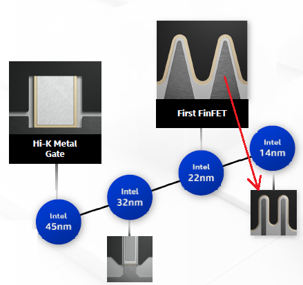
Figure 3. Illustration of the evolution of the FinFET channel profile.
The raised source/drain epitaxial growth regions influence the transistor behavior in multiple ways:
- high concentration impurity introduction for reduced Rs and Rd
- transfer of (compressive or tensile) material stress to the channel region, influencing the free carrier mobility
- an increased gate-to-source/drain parasitic capacitance
The figure below illustrates the additional parasitic capacitances (Cgs, Cgd, and Cgx) due to the three-dimensional geometry of the gate traversal over multiple device fins.
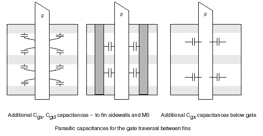
Figure 4. There are unique parasitic capacitances due to the FinFET geometry. The raised S/D epitaxial regions (with M0 interconnect) add to the Cgs and Cgd parasitics.
At each FinFET process node, all foundries have introduced “plus” versions for improved performance.
Intel’s 10nm “SuperFin” process announcement
At the recent Intel Architecture Day, a major kicker to Intel’s 10nm process was introduced.
The Intel presentation initially highlighted the process advancements that were incorporated into the baseline 10nm process, as illustrated below.
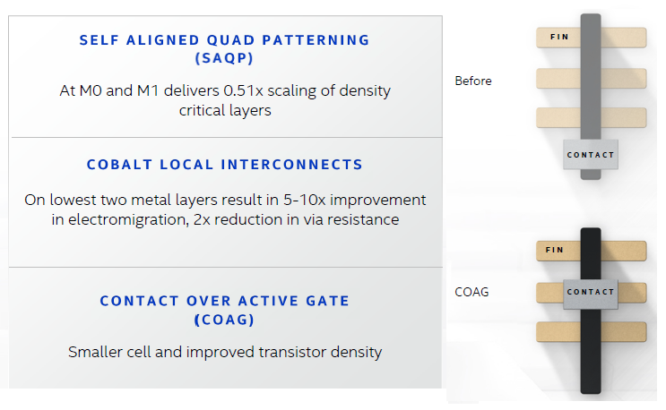
Figure 5. Intel 10nm baseline process enhancements
There were acknowledgements from the presenters that the goals for 10nm process scaling were extremely aggressive, and these corresponding process enhancements took longer than originally planned to reach production yield status.
The new 10nm process variant includes several CPI characteristics:
(1) reduced damascene liner thickness
As illustrated in the figure below, a liner material (of higher resistivity) is deposited on the damascene trench prior to metal deposition for improved adherence. Reducing the requisite liner thickness reduces the effective resistance, thus reducing the total interconnect R*C delay.
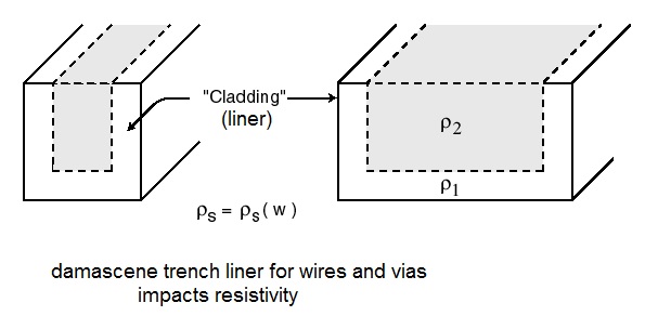
Figure 6. Damascene-based interconnect and via cross-section, utilizing a liner material
(2) new epitaxial S/D growth process
An enhancement to the raised S/D growth process step results in greater material stress in the fin channel, enhancing carrier mobility, and thus device current.
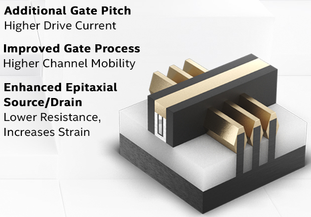
Figure 7. Illustration of the raised S/D epitaxial grown on the S/D sides of the FinFET gate
(3) physical design rule update to support increased gate-to-gate spacing
It may seem counterintuitive that increasing the device gate pitch in circuit layouts would result in a performance improvement. Yet, referring to the FinFET parasitic capacitance figure above, the parasitics are an intricate combination of Cgs, Cgd, Cgx, Csx, Cdx, Rs, and Rd, which depend on both 2D and 3D topologies. (Rgate has already been improved from the introduction of contact-over-active-gate design support.)
When combined with the new raised S/D epitaxial growth and channel stress enhancements, a greater gate pitch could certainly result in better performance.
(4) improved MIM capacitor structure
A significant decoupling capacitance must be connected to the power distribution network (PDN), to reduce power supply rail transients when large switching currents are required. The total decoupling is a composite of both external capacitance (e.g., surface-mount caps on the package), and die-internal capacitance. The internal capacitance consists of the “intrinsic” capacitance of the PDN interconnect (and junction nodes) and the “explicit” decoupling integrated into the design. The explicit capacitance is provided by decoupling cells and a unique metal-insulator-metal (MIM) parallel-plate structure incorporated into the BEOL metallization stack.
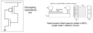
Figure 8. Decoupling library cell and MIM capacitance structure
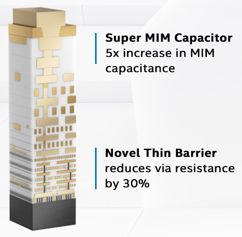
Figure 9. Illustration of the MIM addition to the BEOL
Intel announced an enhancement to the MIM structure in 10nm, providing “5X” improved areal decoupling density.
Although the larger logic gate pitch reduces the die area available for decap cells, the increased MIM capacitance density more than compensates. Indeed, by reducing supply voltage droop, Intel is realizing a net performance gain.
A Cumulative Performance Boost approaching 20%
As was shown in Figure 1, the cumulative performance effect of these 10nm improvements approaches 20% (@ iso-power). The figure below illustrates the typical Ion versus Ioff comparison curves for successive process nodes – the horizontal line depicts the Ion (performance) gain at the same Ioff (leakage power) for a reference device in the two nodes.
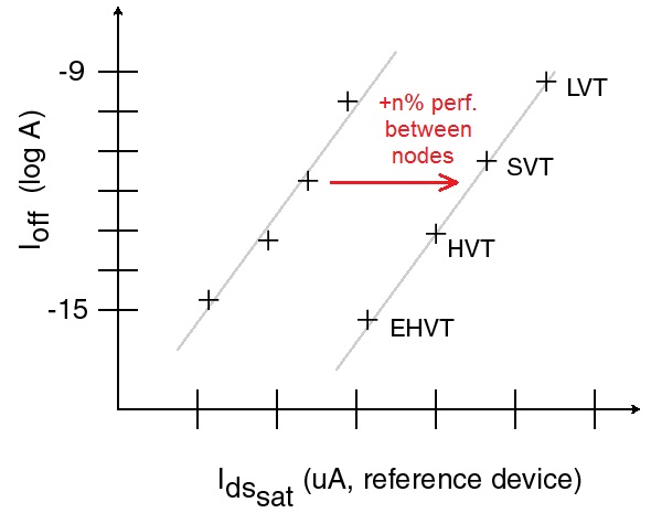
Figure 10. Typical illustration of the Ion versus Ioff curves for two process nodes
The ~20% performance improvement represents the typical gain between successive nodes – realizing this gain as an extension to the 10nm node is a very significant CPI announcement.
The marketing team at Intel has designated this process variant as “10SF”, where SF is short for “SuperFin”. An anecdotal comment was made by one of the presenters, “There were already so many process ‘+’ versions for 10nm, it was getting hard to keep them straight – a new naming convention was needed.
Intel will be releasing their TigerLake mobile client processor family this Fall, using the 10SF technology. It will be extremely interesting to see how the TigerLake PPA compares to other product implementations.
For more information on the Intel Architecture Day announcements, please follow this link. A wealth of presentation videos and materials are available, covering not only the 10SF announcement, but also the latest CPU and GPU architectures, the FPGA roadmap, (2.5D and 3D) packaging technology highlights, and advanced interconnect strategies.
Sources:
Figures 1, 3, 5, 7, 9: Intel
Figures 2, 4, 6, 8, 10: T. Dillinger, VLSI Design Methodology Development
-chipguy
Share this post via:


Comments
One Reply to “A “Super” Technology Mid-life Kicker for Intel”
You must register or log in to view/post comments.