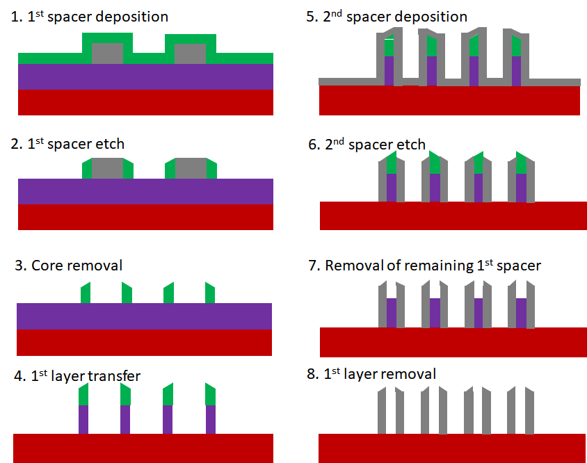
Self-aligned quadruple patterning (SAQP) is the most widely available technology used for patterning feature pitches less than 38 nm, with a projected capability to reach 19 nm pitch. It is actually an integration of multiple process steps, already being used to pattern the fins of FinFETs [1] and 1X DRAM [2]. These steps, shown schematically in Figure 1, allow lines originally drawn 80 nm apart to generate lines which are ultimately 20 nm apart (effectively 10 nm resolution). This is important, as it is well beyond the resolution of any high volume lithography tool, including EUV (13 nm resolution) [3].
Figure 1. SAQP process flow.
Feature grouping
The process naturally categorizes features into three groups: core, shell, boundary (Figure 2)[4]. The shell features naturally form loops which need to be cut. Likewise, the boundary constitutes a mesh which also needs to be separated into segments. Consequently, the SAQP process must conclude with lithography steps which cut or trim previously defined shell and boundary features. By comparison, the older SADP process only has two groups, core and boundary [5].
Figure 2. Separation of SAQP-generated features into core (C), shell (S) and boundary (B) categories. The green indicates the second spacer. The core and boundary features are expected to be made of the same material, while the shell feature is made of a different material.
An alternative SAQP process
Under an alternative SAQP process flow (Figure 3), the shell feature is actually the remnant first spacer material, while the core and boundary are a different material, either the substrate or a gapfill material. Hence, they are indicated by different colors in Figure 2. The fact that they are different materials suggests that they can be selectively etched. This enables some opportunities for hard-to-do patterning [6].
Figure 3. Alternative SAQP process flow, where instead of gaps, different materials fill different regions.
Allowing a prohibited combination
A particularly handy application is the combination of minimum pitch and 2x minimum pitch features. Such a combination is generally forbidden in a single exposure with k1<0.5 [7]. A particularly prohibitive combination would be lines at minimum pitch, with breaks at 2X minimum pitch (Figure 4, left). The diffraction pattern of the line breaks is a much weaker signal than that of the lines themselves, since they occupy a much smaller area. It also degrades faster with defocus [7]. Such a combination also cannot be fixed with assist features [8], as there is no room to insert them for minimum pitch lines. On the other hand, with selective etching, a mask feature is allowed to cross the intervening line in the middle (Figure 4, right). This greatly simplifies the cutting and avoids the edge placement errors that may arise with separated cuts at the two locations [6].
Figure 4. Left: The line pitch and the line break pitch (=2X line pitch) are not compatible. Right: The incompatible pitches may be combined with the assistance of selective etching. In this case, only the material in the blue areas is etched; the red areas are not affected by this mask.
More tractable multipatterning
With selective etching, the use of three masks is a must – one is needed to define the separated A/B regions, a second one is used with A-selective etch, and the third one with B-selective etch. However, selective etching (in combination with SAQP) also makes multipatterning more tractable by allowing more tolerance in overlay and the minimum number of masks to allow the combination of minimum line pitch and line breaks spaced at double the minimum line pitch.
References
[1] https://spie.org/news/6378-self-aligned-quadruple-patterning-to-meet-requirements-for-fins-with-high-density?SSO=1
[3] https://www.asml.com/en/products/euv-lithography-systems/twinscan-nxe3400c
[4] T. Ihara, T. Hongo, A. Takahashi, C. Kodama, “Grid-based Self-Aligned Quadruple Patterning Aware Two Dimensional Routing Pattern,” 2016 Design, Automation & Test in Europe, p. 241.
[5] K. Nakayama, C. Kodama, T. Kotani, S. Nojima, S. Mimotogi, S. Miyamoto, “Self-Aligned Double and Quadruple Patterning Layout Principle,” Proc. SPIE 8327, 83270V (2012).
[6] A. Raley, N. Mohanty, X. Sun, R. A. Farrell, J. T. Smith, A. Ko, A. W. Metz, P. Biolsi, A. Devilliers, “Self-aligned blocking integration demonstration for critical sub-40nm pitch Mx level patterning,” Proc. SPIE 10149, 101490O (2017).
[8] J. G. Garofalo, O. W. Otto, R. A. Cirelli, R. L. Kostelak, S. Vaidya, “Automated layout of mask assist-features for realizing 0.5 k1 ASIC lithography,” Proc. SPIE 2440, 302 (1995).
Share this post via:


Intel’s Path to Technological Leadership: Transforming Foundry Services and Embracing AI