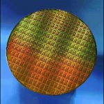
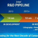
SILVACO 073125 Webinar 800x100

Virtual Platforms plus FPGA Prototyping, the Perfect Mix

Virtual Platforms plus FPGA Prototyping, the Perfect Mix
by Paul McLellan on 06-03-2012 at 8:59 pm

There are two main approaches to building a substructure on which to do software development and architectural analysis before a chip is ready: virtual platforms and FPGA prototyping.

Virtual platforms have the advantage that they are fairly quick to produce and can be created a long time before RTL design for the various blocks is available. They run fast and have very good debugging facilities. However, when it comes to incorporating real hardware (sometimes called hardware-in-the-loop HIL) they are not at their best. Another weakness is that when IP is being incorporated, for which RTL is available by definition, then creating and validating a virtual platform model (usually a SystemC TLM) is an unnecessary overhead, especially when a large number of IP blocks are concerned.

FPGA prototyping systems have the opposite set of problems. They are great when RTL exists or something close to its final form but they are hopeless at modeling blocks where there is no RTL. Their debugging facilities vary since it is not possible to monitor every signal on the FPGA but you never know which ones you need until a bug occurs.

Synopsys have products in both these spaces. Virtualizer is a SystemC/TLM-based virtual prototype. Synopsys acquires Virtio, VaST and CoWare’s virtual platform technologies so somewhere under the hood I’m sure these technologies are lurking. And according to VDC they are the #1 supplier of virtual prototyping tools.

They also have an FPGA based ASIC prototyping system called HAPS, which is also the market leader.

Projects often use both of these. Early in the design cycle they use a virtual platform since there isn’t any RTL. Later, when RTL is nearly complete, they switch to the FPGA approach so that they guarantee that the software is running on the “real” hardware.

Now Synopsys have combined these two technologies into one. That is, part of the design can be a virtual prototype and part of the design can be represented as an FPGA-based prototype. The two parts communicated through Synopsys’s UMRBus which has been around for a couple of years. This brings the best of both worlds and removes the biggest weaknesses of each approach. And, as a design progresses, it is no longer necessary to start in the virtual prototype world and make a big switch to FPGA. It can starts as a mixture and the mixture can simply change over time depending on what is wanted. There are libraries in both worlds, processor models, TLM models, RTL of IP, daughter boards. All these can be used without needing to be translated into the other world.

Here’s an example. A new USB PHY and a device driver. In between a DesignWare USB core, an ARM fast model with some peripherals (as a virtual prototype) and Linux. This can all be put together an run communicating with the real world (in this case a Windows PC).


Understanding and Designing For Variation in GLOBALFOUNDRIES 28nm

Understanding and Designing For Variation in GLOBALFOUNDRIES 28nm
by Daniel Nenni on 06-03-2012 at 8:30 pm

On Wednesday there is a User Track Poster Session that examines the design impact of process variation in GLOBALFOUNDRIES 28nm technology. For those of you who are wondering what process variation looks like at 20nm take this 28nm example and multiply it by one hundred (slight exaggeration, maybe).

Variation effects have a significant impact on nanometer circuit designs. Variation causes performance loss, yield loss, and re-spins, resulting in delayed time to market and financial losses. To address this challenge, GLOBALFOUNDRIES provides variation models that can be used to simulate process variation effects in the design flow. This enables designers to improve their designs and make them robust to variation effects.

This poster session examines the design impact of process variation in GLOBALFOUNDRIES 28-nm technology. Variation effects are compared between GLOBALFOUNDRIES’ 28-nm and 40-nm technologies, as well as between different types of variation within the 28-nm technology. A design example will be discussed that demonstrates the application of variation-aware design in GLOBALFOUNDRIES 28-nm technology.


Solido Variation Designer was used to perform variation-aware analysis and design in this work. Solido Variation Designer is a variation-aware custom IC design tool that leverages variation data in GLOBALFOUNDRIES models to provide efficient, accurate variation-aware design. This tool made it possible to perform thorough analysis in a variety of variation analysis and design tasks, including: fast PVT corner analysis, sigma-driven statistical corner extraction, high-sigma Monte Carlo analysis, identification of variation-aware design sensitivities, and rapid design iteration.

Speaker:
Pei Yao – GLOBALFOUNDRIES, Milpitas, CA
Authors:
Pei Yao – GLOBALFOUNDRIES, Milpitas, CA
Richard Trihy – GLOBALFOUNDRIES, Milpitas, CA
Jiandong Ge – Solido Design Automation, Inc., Saskatoon, SK, Canada
Kristopher Breen – Solido Design Automation, Inc., Saskatoon, SK, Canada
Trent McConaghy – Solido Design Automation, Inc., Saskatoon, SK, Canada
Person of Interest: Daniel Nenni – SemiWiki.com, Silicon Valley, CA


Industry Standard FinFET versus Intel Tri-Gate!

Industry Standard FinFET versus Intel Tri-Gate!
by Daniel Nenni on 06-03-2012 at 6:00 pm

Ever since the “Intel Reinvents Transistors Using New 3-D Structure” PR campaign I have been at odds with them. As technologists, I have nothing but respect for Intel. The Intel PR department, however, quite frankly, is evil. Correct me if I’m wrong here but Intel did not “reinvent” the transistor. Nor did they come up with the name Tri-Gate. If not for prior art, Intel would certainly have trademarked it, my opinion.

As I previously wrote, other than the unique profile chosen by Intel for their Tri-Gate implementation, there really is no key technical distinction between Tri-Gate and the industry standard term FinFET. According to Dan Hutcheson, CEO of VLSI Research, who follows Intel rather closely:

The reason why Intel calls its FinFET a Tri-Gate is that it is a subspecies of the technology. The original FinFET was a bigate. When Intel first developed theirs (way back in the last decade) out of respect for Chenming they named it a Tri-Gate, so as not to draw from UCB’s work. Out of respect? What does that say about the rest of the industry drawing from Chenming’s work that is using the FinFET moniker? Plus, Dan says, the real importance of the Tri-Gate is not so much the third gate, but the fact that it is so much easier to manufacture than a bi-gate. That was the real contribution of Intel.

According to my sources this is not entirely true. The original paper(s) from Chenming’s group at UC-B did propose a “dual gate” (possibly even independent) structure. In the original proposal, the top surface of the FinFET would receive a thicker dielectric than the sidewalls, and not contribute to the device current. If the fin was covered by a single, continuous gate material, that would be a “dual gate”. If the gate material was etched and the sidewalls were covered by separate gates, that would be an “independent dual gate”. (Offering two independent input signals to a FinFET device provides some unique power/performance tradeoff optimizations not available with a single input signal to the transistor.)

However, lots of researchers pursuing FinFET fabrication realized that the “dual” gate (especially the dual-independent option) would be very difficult to fabricate with high yield in production. As a result, technical papers began to emerge with the triple-gate option, where the (thin) gate dielectric was also present on top of the fin, in addition to the sidewalls. The third gate surface on top of the fin is not as effective as the gate on the two sidewalls, as your note indicates.

Here’s an example of some of the triple-gate research:

Burenkov and Lorenz, “Corner effect in double and triple gate FinFET’s”, 33rd Conference on European Solid-State Device Research, 2003, p.135-138.

So, Intel was among many to pursue triple gate FinFET fabrication. And, they were certainly not the only research team to use the term “tri-gate” 10+ years ago:

Breed and Roenker, “Dual-gate and Tri-gate FinFET’s: Simulation and Design”, International Semiconductor Device Research Symposium, 2003, p. 150-151.

So, the use of the term is not really in deference to Chenming or UC-B — it’s a “de facto” standard term that the industry has used for the FinFET fabrication option that Intel has chosen.


Spyglass by Atrenta

Spyglass by Atrenta
by Paul McLellan on 06-03-2012 at 4:27 pm

I’ve been helping get booths set up at DAC in Moscone for the last couple of days. Atrenta’s booth shows their new branding that I talked about last week. Now you can see what they are doing in this picture of their booth. As I sort of guessed they are leading with the Spyglass name. The booth says everywhere “Spyglass by Atrenta.” I don’t know if this is a baby step to eventually rebranding the company as SpyGlass and maybe even they don’t know themselves.

And every morning at DAC they vacuum the carpet so that it is SpyGlass Clean. OK, that was pretty lame…


Did You Know Venus is Transiting the Sun During DAC 2012?

Did You Know Venus is Transiting the Sun During DAC 2012?
by Daniel Nenni on 06-02-2012 at 2:27 pm

On Tuesday, June 5th, starting at 3:05 pm in San Francisco, the planet Venus will cross, or transit, the sun. If you stop by Ciranova’s DAC booth #1608 anytime on Monday or Tuesday, they will give you a free pair of solar viewing glasses that will let you view the transit safely.

According to the NASA website, Transits of Venus across the disk of the Sun are among the rarest of planetary alignments. Indeed, only seven such events have occurred since the invention of the telescope (1631, 1639, 1761, 1769, 1874, 1882, and 2004). Per Wikipedia:

A transit of Venus across the Sun takes place when the planet Venus passes directly between the Sun and Earth, becoming visible against the solar disk. During a transit, Venus can be seen from Earth as a small black disk moving across the face of the Sun. The duration of such transits is usually measured in hours (the transit of 2004 lasted six hours). A transit is similar to a solar eclipse by the Moon. While the diameter of Venus is almost four times that of the Moon, Venus appears smaller, and travels more slowly across the face of the Sun, because it is much farther away from Earth.

Interesting stuff!

Even more interesting is the new Ciranova Helix layout automation solution to enable Agile Layout, a dramatic improvement over traditional, manual layout techniques. Using Agile Layout, IC design teams are able to start layout sooner, refine the circuit based on feedback from layout, and finish layout faster.

Because traditional layout takes so long and is so hard to change, layout designers seldom start before the circuit design is nearly complete. This means that circuit designers must wait weeks or months after their circuit is complete to learn whether the layout will meet performance and area targets.

Using an Agile layout flow, design teams can start layout early, as soon as the first blocks of a design have been completed. Helix produces initial layout results very quickly, so circuit designers can get early feedback on performance, parasitics and area. Layout designers have time to refine their designs and test alternatives, often resulting in smaller, higher-performance layouts. With Agile Layout, layout is usually finished soon after circuit designers finish their last blocks.

Click HEREfor the new Helix FAQ. Then see Helix in action at DAC 2012 booth #1608 and pick up your free pair of solar viewing glasses!


DAC: Advice for Out-of-towners

DAC: Advice for Out-of-towners
by Paul McLellan on 06-01-2012 at 6:53 pm

I blogged several times over the last few weeks about places in San Francisco other than DAC at the Moscone Center. Since they are now spread all over the site it is not so easy to find them. So here they are again all in one place.

Places to eat and drink near the Moscone center

Interesting San Francisco bars

Where to get the best coffee

Eating in San Francisco

Other things to do in San Francisco, how to be a tourist

Have a great time in San Francisco, it’s a great city.


DAC: there’s an App for that

DAC: there’s an App for that
by Paul McLellan on 06-01-2012 at 5:00 pm

Bill Deegan has produced a new version of his iPhone DAC app for this years conference. You can download it for free from the Apple App Store here. It is basically a mobile version of the DAC conference brochure with schedules for the various events (which it can add to your calendar if you decide you are interested) and the floorplan of the tradeshow.

Last year the App was iPhone only but Bill has also been working on an Android version. It should be available sometime over the weekend. I’ll update this blog entry with the link when there is one.

UPDATE: Android App is here.

UPDATE: The events database now has the evening cocktail receptions. To ensure you’ve loaded the latest events data please do the following: Navigate to DAC49 apps’s home screen. Click on “Events By Title”, click back to home screen, and then click “Events By Title” again.


Apple Will Build In America

Apple Will Build In America
by Ed McKernan on 05-31-2012 at 8:10 pm

As Apple races towards $200B in revenue, sometime in 2013 and perhaps $300B by 2015, Tim Cook knows it is in Apple’s best interests to start building a sizeable percentage of iPhones and iPADs in the US and soon. At the All Things D conference this week, Walt Mossberg asked Cook about Apple’s manufacturing presence in China and “if Apple envisions having big manufacturing in the U.S.?” To which Cook said: “I want there to be.” He then proceeded to communicate that someday assembly could be moved to the US and that “We should do more semiconductor things in the U.S.” I read this as a strategy that leads to a significant differentiator relative to Apple’s competitors (i.e. Samsung, HP and Dell).

For Apple to extend its lead amongst competitors, it must continue to build Brand Equity and Goodwill in all the regions of the World that it sells its products. Soon that will include all six continents. Goodwill can be built by expanding its presence into a number of communities in the form of jobs and charity. Austin is home to some of Apple’s planned expansion and the Samsung fab that builds the processors powering the range of iOS devices. Discussions at the school boards now include buying iPADs for elementary and middle school kids. Dell PCs are not being considered.

Expand that thought to include the Federal Government and every statehouse and your talking about a huge market expansion that awaits Apple in the coming years. One way that Apple can make the transition easier from PCs to Apple iPADs, MAC Airs and iPhones is by letting the buyers know that a majority of the components are made in America as well as final assembly being completed here. Dell and HP will not have the financial flexibility to follow in Apple’s path nor will Microsoft be able to stop the train as it leaves the station.

Apple’s meteoric rise has caught many by surprise but to go this next step, building in America, is reminiscent of Toyota and Honda’s rise in the 1970s and 1980s. The demand for their cars was so great that Detroit was about to go under save for government imposed import restrictions on cars and 25% tariffs on trucks. The Japan automakers got the message and began transplanting assembly plants across a number of states with local suppliers included. The import quotas were made moot.

What does this mean for the semiconductor industry? As Apple has imposed labor work rules in Chinese plants, expect that they will also impose supplier requirements that meet their long-term strategic goals. I believe it when Tim Cook says he wants to source more semiconductor components from the US and that he wants to eventually set up assembly here. The Goodwill he generates will vault Apple past his current competitors and even more important, past Samsung. Look for Apple to fab with Intel in a US plant on preferential terms. I think price is what keeps Apple out of Intel today, but this will change. Look for a closer relationship with Micron for DRAM and NAND Flash. Other suppliers like Qualcomm, Broadcom and Cirrus may have to build at Global Foundries in New York unless TSMC sets up shop in the US. To not build in the US brings many downside scenarios in play with Apple that would more than offset any manufacturing cost increase. Time to be proactive and grab the ring.

Finally, a point that has to be highlighted to understand the ruminations of this blog. It is the background of Tim Cook, son of a shipyard worker from Robertsdale, Alabama and once a worker in a Paper Mill plant and Aluminum factory that has caught my attention. I come from an area of the country that, like Cook’s, was heavy blue collar based. And one summer, I too worked in a Paper Mill (in Pennsylvania). When you grow up in these surroundings, you always feel the tug to do something that is meaningful not just in Silicon Valley but in the rest of America. I believe this is what is driving Cook’s vision in making Apple the World’s Greatest Corporate Citizen. A part of this vision means bringing the computer industry back to America. It would be a huge gift to this country if we end up several years from now where we began in the 1970s. I believe we just witnessed the first sketches on the canvas of Tim Cook’s long-term plans.

FULL DISCLOSURE: I am Long AAPL, INTC, QCOM, INTC