Mobile applications require CMOS image sensor devices that have a low signal-to-noise ratio (SNR), low power, small area, high resolution, high dynamic range, and high frame rate. CMOS image sensor imaging performance is noise limited requiring accurate noise analysis on the pixel array electronics and column readout circuitry.
Image sensor noise sources can be categorized as spatial and temporal noise sources. Spatial noise sources include dark fixed pattern, light fixed pattern, column fixed pattern, row fixed pattern, defect pixels, dead and sick pixels, scratches, and so on. In the case of dark fixed pattern, the dark current becomes very small in deep nanometer processes and its effect is typically not noticeable during normal pixel operation.
Temporal noise is random in nature and fundamentally limits image sensor performance. Temporal noise includes kT/C noise, flicker noise (1/f), dark current shot noise, photon shot noise, power supply noise, phase noise, ADC quantization noise, and so on. Temporal noise dominates the pixel random noisefloor and is the main source of noise in the readout circuitry.
With the Berkeley Design Automation Analog FastSPICE (AFS) Platform, designers can use transient noise analysis to verify the impact of temporal random device noise on the readout circuitry, including ADCs and comparators, with nanometer SPICE accuracy. In addition, designers can include post-layout parasitics and characterize the circuit for process variation and device mismatch.
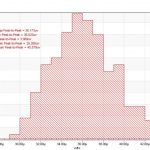
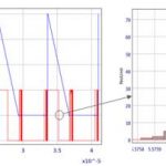
In the case of comparators, as illustrated in the plots, AFS transient noise analysis quantifies absolute jitter in the trigger point with nanometer SPICE accuracy. This accuracy is important, because the comparator is a sharp transition circuit where small noise can cause large waveform perturbations.
For full-circuit functional verification of CMOS image sensor devices, the AFS Platform has the accuracy, performance, and capacity to handle multiframe verification of a representative subset of the full array and readout circuitry with nanometer SPICE accuracy.
Further reading: CMOS Image Sensor Verification Hot Topic:
http://www.berkeley-da.com/prod/hot_topic_req.html
Berkeley Design Automation, Inc. is the recognized leader in nanometer circuit verification. The company combines the world’s fastest nanometer circuit verification platform, Analog FastSPICE, with exceptional application expertise to uniquely address nanometer circuit design challenges. More than 100 companies rely on Berkeley Design Automation to verify their nanometer-scale circuits. Berkeley Design Automation was recognized as one of the 500 fastest growing technology companies in North America by revenue in 2011 and again in 2012 by Deloitte. The company is privately held and backed by Woodside Fund, Bessemer Venture Partners, Panasonic Corp., NTT Corp., IT-Farm, and MUFJ Capital. For more information, visit http://www.berkeley-da.com.
lang: en_US