BannerforSemiWiki 800x100 (2)

Xilinx’s UltraScale vs Arria 10 – Non dolet, Paete

Xilinx’s UltraScale vs Arria 10 – Non dolet, Paete
by Luke Miller on 03-18-2014 at 9:30 pm

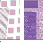
The DSP48E2 (I do not come up with these names… Could have named it a multiplier thingy) in the Xilinx 20nm UltraScale family (I do not come up with these names… Could of named it Virtex-8, or Luke-8) is simply amazing. Today was good, as I began playing with UltraScale tools and seeing how the DSP checks out. I also encourage you to check out the Altera 20nm node and you will once again see quite a difference between the families. In fact Altera says they are ‘redefining the midrange’ at the 20nm node… and for the Stratix-10, ‘Delivering unimaginable performance’. I am holding back on that one, in fact dear reader you could add in the punch line here. I was humming ‘it’s a small world after all’, picturing tattoo from Fantasy Island, yelling De FPGA, De FPGA Boss!

Xilinx claims that the complex multiplier in the 20nm UltraScale will need ½ the DSP resources it needed in the 28nm node. That is a big deal, as in my field, RADAR/EW complex multiplication is important. For example, the wife asks me to cut her hair. That is input A, input B is I keep saying no but decide to do it. The output C is a very complex situation that involves sobbing, and that is me sobbing. That is a true story by the way (No I didn’t cry, I embellished a bit), and it turned out exactly like I said it would. My dear, dear Manly reader, may I suggest you never cut your wife’s hair, ever. My dear, dear feminine reader, do not ask your man to style your hair, you will really regret it and will take 3 months to forgive your guy. I know, pray for my family.

In the UltraScale 20nm Kintex 115, we have 5500 DSP. There are 3600 DSP in the largest 28nm Virtex-7 FPGA, so you say ‘well that is only a 1900 DSP increase.’ I say you spoiled designer you! Remember the Virtex-2 Pro Days, with a whopping 232 18×18 multipliers, see how you are spoiled? Ok, the 1900 DSP increase in actually much more than that when you factor in clock frequency, bit widths, and efficiency. For most configurations, the complex multiplier that used 8 DSP slices in 28nm will only need 4 DSP in UltraScale 20nm. That is 1900 + 2X GMACs gained when performing complex multiplies.

For example, if you wanted a system that needed 1375 18×27 complex multiplies you could do this in one UltraScale Kintex-115. Altera’s Arria-10, would need 1.63 Arria’s. And I know it is very hard to purchase a 0.63 FPGA so I think you need 2 Altera FPGAs. Altera’s Data sheet says you need 2 Variable DSP’s for one complex multiply and there are 1678 Variable DSPs, that means you can only have 839 complex multiplies. 1375/839 = 1.63.

Wait… Now wait! Hold, hold…hold.. On here… in a George Bailey voice. This is for an 18×27 Complex Multiply, and the 1.63 Arria’s was for 18×19…Well I was conservative, and I did not even discuss gigabit transceivers. But the Xilinx KU115 can move 2 Terabits over 64 x 16 gb/s Transceivers. Arria-10, not so much with 48 x 17.4 gb/s transceivers = 1.67 Terabits.

Xilinx KU115 = 5520 DSP x 741 MHz x 2 = 8180 GMACs
Arria10 GX660 = 3356 DSP x 500 MHz x 2 = 3356 GMACs

Arria base multipliers are 18×19 and Xilinx is 18×27, this means as in most systems you will need to use more multipliers to achieve most applications. How many systems do you know that use 18×19 for filter applications? Most systems have digital processing gain that effectively use the Xilinx DSP slice. Xilinx’s DSP is close to 3X better than Altera.

By the way a history lesson from Wikipedia, reader beware, the Name Arria:

“Arria (also Arria Major) was a woman in ancient Rome. Her husband Caecina Paetus was ordered by the emperor Claudius to commit suicide for his part in a rebellion but was not capable of forcing himself to do so. Arria wrenched the dagger from him and stabbed herself, then returned it to her husband, telling him that it didn’t hurt (“Non dolet, Paete!”). Her story was recorded in the letters of Pliny the Younger, who obtained his information from Arria’s granddaughter, Fannia.

Ok..Right… Let’s name an FPGA after a lady who stabbed herself to prove it didn’t hurt to her husband. Sounds like me cutting my wife’s hair! – Non dolet, Paete.

Anyways, Xilinx of course has all your FPGA ranges covered, they call it the ‘low end series’ (I assure you I do not come up with these names, Low End? Arria? How about Super Duper Value FPGA?). Looking at Xilinx’s 28nm, 20nm, there is no other device that comes close to it. So you are using Altera why? Can someone explain to me where the measurable advantage is? How about TI’s DSP chips, why? You can program Xilinx’s FPGAs using C/C++ very easily which excellent QoR, and Floating Point for Xilinx FPGAs are trivial. Considering GPU’s? Think again about using FPGAs SEU, Power and Reliability are many times better than GPUs. Xilinx clearly is the leader in the FPGA realm and it did not happen by accident. Check them out today, you will not be disappointed.

lang: en_US


Atmel on Tour at AT&T Park

Atmel on Tour at AT&T Park
by Paul McLellan on 03-18-2014 at 5:02 pm

OK, it’s not exactly AT&T park…it’s the parking lot. But they have a huge semi loaded up with lots of cool Atmel stuff to show off some of the things that their customers are doing with their microcontrollers and display technology, primarily focused on the internet of things (IoT). I went down to check it out, which would have been a lot easier before I moved house since they are a few hundred yards from my old place. They will be in Napa on 23-242th March and then Las Vegas on 26th. There are lots more cities too.


First up is one of the smart watches (coincidentally Google just announced their entrance into this market today too). It contains two Atmel microcontrollers, one ARM Cortex to do the work and another 8-bit AVR microcontroller to handle I/O and to wake up the application processor when there is work to be done. It also has a wireless charger (on the left) which is a good idea given that the watch is waterproof and so the case can be completely sealed.

Next up was some Philips technology for controlling dozens of lights for color and brightness from an iPad. Each bulb (actually an LED or a strip of LEDs) has a Zigbee mesh network microcontroller and can vary its color across the spectrum.


Then a Black and Decker cordless drill. One problem companies in the power tool business have is that they would like their tools to only work with their batteries. They obviously have a financial interest in doing this but it is a huge liability problem too. Their products tend to be build overseas and sometimes the designs get stolen and batteries with crummy cells or electronics are sold as genuine. And it is Black and Decker that gets sued when one of these catches fire, which is a real issue with battery control. The bigger the battery, the bigger the problem. In fact it is one of the things that Tesla had to focus on to build power packs the size they need using the same lithium-ion technology used in cellphones, laptops and cameras. Using a chip that costs well under $1 with Atmel’s security software it is possible to make batteries that authenticate. They communicate over the power lines when the battery is changed and if the authentication fails with either the drill or the charger then it simply will not work. Some of the inkjet printer manufacturers have started to do this too, to ensure that only genuine cartridges are used, since their business model depends on cheap printers and making money on ink. Putting up the cost of the printer cuts their market share a lot but not selling ink means they can’t make money.


Finally a technology I’ve seen before, which is Atmel’s flexible display technology called Xsense. The touchscreens look exactly like the transparencies we used to use on overhead projectors, although actually a bit thinner. They can be flexed in use although the initial applications seem to tend more towards being able to build screens that are not flat: watches that wrap around your wrist, curved tablets and so on.


They also had a 3-D printer. I’ve written before how Atmel has over 90% market share of the microcontrollers for this market. As the prices come down, these are clearly going to get much more widely available. The one they had printed in plastic (you can also get them that print metal and how about this one printing a house out of concrete, in 24 hours).

Later there was a panel session on Internet of things with people from Atmel, ARM, Humavox (wierless charging) and August (IoT door locks). I won’t try and describe the whole panel, this blog is already too long. The most interesting aspect was that everyone was very concerned about security and privacy. After all, if you control the door lock through your smartphone you want to make sure nobody else does, and you probably don’t want just anyone to know all the times at which you come and go. Especially if they can correlate that with where your self-driving car took you, who you called and so on. As more and more data ends up in the cloud, this will be a bigger and bigger problem. There was also a worry about small companies being taken over by the likes of large ones: you may not care that Google knows the temperature in your living room, but you probably do care if they know everything above and can sell that information to monetize it.

Full details of Atmel’s Tech on Tour are here.


More articles by Paul McLellan…


Social Media at Carbon Design Systems

Social Media at Carbon Design Systems
by Daniel Payne on 03-18-2014 at 11:12 am

Started in 2002 Carbon Design Systems has ESL (Electronic System Level) modeling and validation tools for complex SoC design. With their software you can:

  • Perform system level model generation of existing and 3rd party IP directly from RTL for use in any virtual platform
  • Do performance analysis & optimization of SoC architectures
  • Enable pre-silicon firmware debug

Continue reading “Social Media at Carbon Design Systems”


Mentor U2U Is On April 10th

Mentor U2U Is On April 10th
by Paul McLellan on 03-17-2014 at 7:19 pm

If you are a Mentor user, U2U, the Mentor User group is coming up on April 10th. This is an all day event at the DoubleTree. The event is free. Registration starts at 8am and the agenda itself starts at 9am. There is a reception from 5-6pm in the evening.

There are three keynotes. At 9am: Wally Rhines, CEO of Mentor. The Big Squeeze. For decades, we’ve known it was coming and now it’s here. Moore’s Law—which is really just a special case of the “learning curve”—can no longer drive the 30% per year reduction in cost per transistor, beginning with the 20/16/14 nm generation. Either we find innovations beyond just shrinking feature sizes and increasing wafer diameter or we slow our progress down the learning curve, introducing innovative new electronic capabilities at a slower rate than in the past. There are lots of alternatives, including a reduction in profitability of the members of the supply chain, to keep the progress continuing at the same rate as the last fifty years.

At 10am: Ashok Krishnamoorthy, the chief technologist at Oracle (the part that used to be Sun Microsystems). Optical Interconnects at a Turning Point – The Opportunity and Prospects for Silicon as a Photonics Enabler. Interconnect will play a major role in overall system performance and energy consumption for future computing systems. Current optical links can provide the required bandwidth, but are relatively expensive and power-hungry. VCSEL-based optical modules can improve the situation greatly, and will help optical interconnects penetrate deeper into computing systems. Recent advances in high-density, ultra-low energy silicon photonic links are likely to make them the preferred solution in the long term as density, bandwidth, and energy efficiency are jointly optimized.

At 1pm: Shawn Han, VP Foundry Marketing at Samsung. Solutions to Smart Mobile Devices. Samsung have done a great job in becoming a real force in foundry, most famously making most of Apple’s Ax chips. Expect them to be come even more of a force at 16nm. This is billed as a “special session” rather than a keynote so I have no idea what to expect.

Outside the keynotes, the day is organized into 8 parallel tracks: Calibre I and II, CustomIC/AMS, Place & Route, Silicon Test and Yield Analysis, Functional Verifications, PADS, PCB.

Some talks that look especially interesting looking are:

  • How to achieve fast power and ground analysis at the full chip level (Broadcom)
  • How to design and verify silicon photonics components (University of British Columbia)
  • How to take advantage of the TSMC9000 IP reliability program (TSMC Technology)
  • Achieving required power, performance, area (PPA) on ARM cores (ARM)
  • How Sherlock Holmes and Dr. Watson Track Down a Yield Limiter (Aptina Imaging)

The full detailed agenda is here(pdf). Free registration is here.


More articles by Paul McLellan…


A Fill Solution for 20nm at TSMC

A Fill Solution for 20nm at TSMC
by glforte on 03-17-2014 at 5:12 pm

By Jeff Wilson, Mentor Graphics

We’ve talked about the new requirements for Fill in IC design for advanced nodes in previous blogs on this site. This time I’d like describe the fill solution that Mentor and TSMC have jointly developed to meet the requirements of fill for TSMC’s 20nm (N20) manufacturing process.

The traditional purpose for metal fill was to improve planarity in the chemical-mechanical polishing (or planarization) process. However, at advanced nodes fill is also used to manage effects related to electrochemical deposition (ECD), etch, lithography, stress, and rapid thermal annealing (RTA). TSMC’s N20 design rules require fill shapes to be evenly distributed and also require a greater variety of fill shapes (see figure). Designers need to add fill not just to metal layers, but also to poly, diffusion, and via layers. Other requirements of the newer technologies include analysis of density gradients, as well as absolute density. Additional constraints include perimeter and uniformity of fill spanning multiple layers. In many cases, multiple fill layers are interdependent.

Comparison of Front-End of Line (FEOL) fill at 65 nm and 20 nm. Fill shapes are no longer just squares, but now require support for multiple layers with a specific pattern to achieve higher density targets. (source: Mentor Graphics)

The collaborative solution from TSMC and Mentor for TSMC’s N20 fill requirements uses the Calibre® YieldEnhancer product’s SmartFill technology, which performs fill and analysis concurrently to ensure that the fill patterns meet TSMC’s forbidden pitch, multi-layer fill, and double patterning rules. Concurrent analysis of the layout also helps designers ensure that timing constraints are met by balancing the amount of fill against unwanted parasitic effects (i.e., added capacitance) as the fill process is being performed. The addition of double patterning (DP) at N20 also adds a new dimension to fill. Metal fill, like all the shapes in the layout, must be colored and decomposed into two masks. Fill observes DP rules to balance the light emitted through the mask to improve design uniformity.

Implementation of these requirements for 20nm required new technology development for SmartFill in the areas of core algorithms, support for multi-layer fill shapes and shape groupings, and repeatable cell-based fill patterns. The SmartFill solution uses the Calibre interfaces to integrate with full custom environments like Pyxis, Virtuoso, and Laker, and place and route tools such as Olympus-SoC, IC Compiler and Encounter to support net-aware fill. Designers can provide a list of critical nets that receive special treatment during the fill procedure and the filling engine can make informed fill placement decisions based on both the type of signals and which signals are timing-critical.

A key advantage of the SmartFill solution at TSMC is that it allows designers to meet IC fill constraints in a single pass with reduced impact on circuit performance and no manual intervention. The approach produces a relatively small post-fill GDS database size, which enables faster data transfers and quicker turnaround times, and the implementation fits into existing design flows to support final timing verification.

References
For more detail on the fill solution used at TSMC for 20nm, download the related white paper, “Advanced Filling Techniques for N20 and Beyond – SmartFill at TSMC.”

Author
Jeff Wilson is the DFM Product Marketing Manager in Mentor Graphics’ Calibre organization. He is responsible for the development of products that address the challenges of CMP and CAA. He previously worked at Motorola and SCS. Jeff received a BS in Design Engineering from Brigham Young University and an MBA from the University of Oregon.


GSA Silicon Summit Is On April 10th

GSA Silicon Summit Is On April 10th
by Paul McLellan on 03-17-2014 at 1:01 pm

The annual GSA Silicon Summit is coming up in a few weeks. It is on April 10th at the Computer History Museum. Registration is at 9am and the meeting itself gets started at 9.45am. The summit finishes at 2.15pm. There are three sections during the day, and lunch is provided.

The first section is on Advancements in Nanoscale Manufacturing. The session will open with an overview detailing the challenges of continued gate scaling, as well as the industry’s exploration of alternative materials and processes in the fabrication of nanoscale structures and the resulting applications that may be enabled. A Panel Discussion will follow to address some of the challenges involved in implementing alternative CMOS solutions as well as recent advancements made in nanoscale engineering. It is presented and moderated by Joe Sawicki of Mentor. The panelists are Dan Ambrush of Sematech, Rob Aitken of ARM, Paul Farrar of the Global 450mm consortium, Peter Huang of TSMC and John Kibarian of PDF solutions.

The second session is on Innovative Solutions. The session will open with an overview on how manufacturing and packaging innovations are allowing improvements in semiconductor design, driving increased functionality and performance to fulfill new opportunities arising in the digital economy. A Panel Discussion will follow and explore the current and future advances of integrating digital, RF, analog/mixed-signal, memory and sensors in close proximity to achieve increased performance from a scaling, material and process perspective. It is presented and moderated by Gary Bronner of Rambus. The panelists are Jim Aralis of Microsemi, Charlie Cheng of Kilopass, Peter Gammel of Skyworks, Lawrence Loh of Mediatek and Mark Miscione of Peregrine Semiconductor.

After lunch the third session is on Enabling a 2.5D/3D Ecosystem. Holding great promise for enabling heterogeneous integration and reducing design complexity, the session will provide an overview on where the industry stands in terms of developing and commercializing 2.5D/3D technology and what remains to be done. A Panel Discussion will follow and address the use case for utilizing 2.5D/3D technology, as well as the business needs within the supply chain in order to ignite 2.5D/3D adoption and market growth, changing it if possible, from a nascent alternative to a mature option. The session is presented and moderated by Javier De La Cruz of eSilicon. The panelists are Calvin Cheung of ASE, Gil Levy of Optimaltest, Bob Patti of Tezzaron, Riki Radojcic of Qualcomm, Arif Rahmen of Altera and Brandon Wang of Cadence.

The detailed agenda, including a link for registration, is here.


More articles by Paul McLellan…


The Technology to Continue Moore’s Law…

The Technology to Continue Moore’s Law…
by Eric Esteve on 03-17-2014 at 11:59 am

Can we agree about the fact that the Moore’s law is discontinuing after 28nm technology node? This does not mean that the development of new Silicon technology, like 14nm or beyond, or/and new Transistor architecture like FinFET will not happen. There will be a market demand for chips developed on such advanced technologies: mobile applications or high performance computing to name a few. These applications exist, where more IP (multiples CPU, GPU, SRAM and various “functions”) have to be integrated into a single SoC, running faster than the previous generation but with a better power efficiency. But, when you add to this specification that a single SoC (platform) will have to ship by several dozen of million units, if not hundred, to fit with economics requirements, you realize that only a few applications will be concerned, not the majority. We have seen in a previous blog that the entry ticket for 14nm FinFET was close to $200 million (International Business Strategies, Inc. 2013 report). When you take a look at the picture below, you realize that the Manufacturing Fabs CAPEX (normalized to 1K Wafer per week) has increased by 86% from 28nm planar to 14nm FF. Going further in technology is possible, and will happen, but no more according with Moore’s law. We may even mention the last node marking Moore’s law limit, it’s 28nm!

So, what will happen to the mainstream semiconductor industry, in order to benefit from Moore’s law similar dynamic, if targeting smaller technology node is no more the solution, as it was for now the last 50 years? Our industry will have to be smart! We could say smarter than Moore!

There are certainly solutions, and most probably more than one track to explore. Smart packaging can be a way to increase density (board density instead of chip density), if you place side by side (2D) or pile up (3D), also lowering power dissipation, as the chip to chip interconnections will be shorter and far less capacitive inside the package, thus C*V[SUP]2[/SUP] will decrease. Another approach, directly linked with Silicon processing, can make sense: targeting Fully Depleted Silicon On Insulator (FD-SOI) technology. If you take a look at the above table, you can see that blindly following Moore’s law from 28 bulk, to 20nm bulk and 14nm FF lead to a performance improvement but also a cost increase. The reasons are process related, as we can see on the next picture:

The Bulk transistor architecture that we are using for decades is reaching limits at 20nm. These limits are linked with the law of physics, and lead to the following issues:

  • Transistor Channel Level: High Cost process flow and more critical process steps (impacting yield, then cost too)
  • Heavily Doped Wells (left of source, right of drain): High variability, forcing to a longer minimum gate length and severe layout limitations (impact on density, design becoming more and more complex to handle)
  • high leakage current: this one is a severe limitation, as it can annihilate the benefit gained on dynamic current improvement
  • Weak process compensation: in fact, the design/process co-optimization is low; we will see that Forward Body Bias effect in FD-SOI is a very smart way to compensate the process related variations, which exists whichever the technology.

Then, we can clearly see two possible routes. The closer to the previously known as Moore’s law is to design a FinFET transistor architecture, and to move one technology node further, leading to 14nm FF (apparently 20nm will not be used for long). We will see on the next picture the cost impact of this 3D technology. The other route is to manipulate the Silicon substrate and create a thin buried oxide, the FD-SOI technology, and stay with 2D (planar) architecture, moreover, stay with 28nm gate length!

If you compare the number of mask layers, and even more important the number of critical layers, 14nm exhibits 66% more critical layers than 28nm. Not a surprise, 14nm FF process will cost 38% more than 28nm. This is the right time to remind that SOI wafer cost is $500 higher than regular wafers. If you want to make a complete cost analysis, you also have to remind the 86% CAPEX increase to build the wafer fab! If you remember the wafer cost analysis published a while ago, CAPEX is a pretty heavy part of a processed wafer cost. If you multiply CAPEX by 1.86, that means that you will have to sell 86% more 14nm FF wafers than 28nm FDSOI to compensate this over CAPEX! Or you just say that 14nm FF is more expensive than 28nm FDSOI…

Thus, can we already say that FD-SOI is smarter than Moore?

Let’s take a look at these few examples: (1) CPU, GPU and Logic, (2) Memories and (3) Analog & High-speed, and try to analyze the FD-SOI benefits in respect with 28nm Bulk.

  • CPU, GPU and Logic: here we search for high performance, and power efficiency. FD-SOI technology exhibits excellent leakage power behavior (in fact, there is no source to bulk or drain to bulk leakage!), and the dynamic power can be lower by 30% (at equivalent performance, as described here), we can tick the power benefit. Performance: we have written about this high speed data networking ASIC, designed by a chip maker claiming for a 30% performance improvement, thanks to the Forward Body Bias effect. By the way, you can benefit from one of these 30% at the same time, or decide to optimize for the best performance to power efficiency, for a mobile application for example…
  • Memories: again the Silicon On Insulator technology direct benefit is the lower leakage compared to bulk, thus a SoC designer may optimize the architecture of an embedded IC, integrating more memory or designing for lower power.
  • Analog & High-speed: almost any SoC will integrate Analog (ADC or DAC) or High-speed PHY to support interface protocols (DDRn, USB 3.0, PCIe etc.). Paul has shown in this blog that FD-SOI analog performance is far beyond bulk one. This is going with a better figure of merit for high-speed IP.

So, can we say that a technology that exhibits lower cost than Bulk HPM & FinFET, a better reliability and yield, thanks to true process compensation through body bias and flexibility of usage is smarter than Moore? I would guess so…

From Eric Esteve from IPNEST

More Articles by Eric Esteve…..

lang: en_US


Xilinx & Apache Team up for FPGA Reliability at 20nm

Xilinx & Apache Team up for FPGA Reliability at 20nm
by Pawan Fangaria on 03-17-2014 at 12:00 am

In this age of SoCs with hundreds of IPs from different sources integrated together and working at high operating frequencies, FPGA designers are hard pressed keeping up the chip reliability from issues arising out of excessive static & dynamic IR drop, power & ground noise, electro migration and so on. While the IPs are tested and verified in isolation, their real test begins when all types of IPs (digital, analog, mixed-signal etc.) interface with each other and works together inside an SoC. An integrated analysis, verification and optimization methodology must exist, not only for the chip but also with package and board included, that can sign-off the system for power noise reliability as well as electro migration (EM).

Although the electrical concepts for verifying these appear to be simple, large design sizes with varying degrees of complexities including mixed-signal, multi-voltage, low noise margin etc. make the task a great challenge for designers. The static IR drop works on DC pattern (with average current); it is good to determine early gross weakness of the design but cannot represent true transient noise analysis. Dynamic transient analysis takes into account the actual leakage and transient switching currents. Typically the P/G network is extracted into RLC circuit and Spice level simulation is done for transient noise analysis. However, due to large size and complexity of RLC network, using Spice is not a viable alternative. Fast-Spice simulators have appeared, yet they may not be sufficient to complete the P/G analysis for large SoCs in a reasonable time and can have issues with their methodology in identifying IR and EM bottlenecks.

Xilinx
has developed an integrated comprehensive single pass flow for static and dynamic voltage drop analysis both at IP as well as full-chip level. It uses Apache’sTotem and RedHawk platform for analysis and simulation.


[Static and Dynamic Voltage Drop Analysis Flow]

IP data is provided in GDSII layout, Spice netlist in DSPF/SPEF format, and testbench or input vectors in Spice format. For an IC or SoC, package layout is also needed. Also, technology parameters in industry standard format (iRCX, nxtgrd), device model data, and layer mapping information are required. Simulations are performed with pre-characterization and layout data; then analysis is done for any design weakness or hotspot. Interactive fixing and analysis are done to resolve issues and then a clean transistor level model is written out for full-chip level analysis. This flow is able to perform analysis for large IPs while maintaining Spice level accuracy by using several techniques.


[Circuit Modeling Detail]

The non-linear nature of the circuit is transformed into linear by pre-characterizing the current, intrinsic resistance and device capacitance for each transistor and replacing every transistor by its own model. The RLC elements of P/G network and associated package/board are extracted and simulated for P/G noise in the circuit. The transistor models act as current sink while parasitic network provides the impedance. The capacitance can come from various sources such as P/G mesh, device diffusion and gate, signal line, and on chip. The linear circuit is then solved by proprietary solver technology and voltage/current can be obtained at every wire, via and transistor.


[GDSII Modeling and Simulation Flow Using Totem]

GDSII
data is used to create model of the power and ground geometries along with the locations of transistors. A high performance & capacity RLC extraction engine (that exploits the regularity in P/G mesh) is used to obtain the parasitic of the P/G network for all power domains with selective inclusion of capacitance and inductance of the mesh as needed (not needed for static analysis).

For static analysis, an average or peak device current is used and the DC voltage/current is computed for each wire and via starting from the voltage sources to the transistors. For transient analysis, the true characterized transient current profile is used along with the associated effective transistor resistance and capacitances and time-domain current and voltage waveforms are computed for each wire and via.

The electro-migration for wires and vias is simultaneously determined based on the current flowing through the P/G mesh and violations checked against the limits defined in the technology file. For static analysis, DC or average EM limits are checked. For transient analysis, average, RMS and peak EM limits are checked.


[Signal EM Analysis with Vectored Approach]

The signal interconnect EM is verified in a similar manner where switching currents for transistors connected to signal nets are pre-characterized and used to model the average, RMS and peak currents on a signal net and compared against the limits specified in the technology file. This can be done in vectored as well as vector-less approach. In vector-less approach, the current waveform at a driver output is constructed based on certain basic parameters provided for a net under analysis. The vector-less approach can be used to gain 100% coverage and be able to sign-off EM on each signal net in the semiconductor design.

By aligning with the bottom-up approach of FPGA designs where IPs are developed separately and integrated together, this methodology promotes IP reuse. The challenge is to perform IP level validation and then model top level connectivity with IP level design constraints such as maximum allowable voltage drop. The CMM blocks can be used for full-chip analysis of mixed-signal design without compromising accuracy and runtime.

More details of this methodology can be referred in a technical paperjointly authored by Sujeeth Udipi at Xilinx and Karan Sahni at Apache, and presented at DesignCon 2014.The paper also suggests about the type of analysis required for different types of design styles in order to save time without loss of accuracy.


More Articles by Pawan Fangaria…..


Cadence is all about Semiconductor IP!

Cadence is all about Semiconductor IP!
by Daniel Nenni on 03-16-2014 at 9:00 am

Cadence continues on its quest to be a top semiconductor IP supplier which is a good thing since the semiconductor world now revolves around IP. Cadence CEO Lip-Bu Tan mentioned IP 14 times during his keynote and he was followed by the president of Imagination Technologies and the CEO of recently acquired Tensilica. I was not afforded the slides for these presentations so we will leave it at that for now. I did sneak a quick photo of this slide which is a nice overview of the current Cadence IP offering.


Semiconductor IP will also be a focus at the IEEE EDPS conference next month. Last year I organized FinFET day, this year it will be IP day:

If you look at the Semiconductor IP usage trends over the last five process nodes (65nm, 40nm, 28nm, 20nm, 16nm) the number of unique IP per tape-out is increasing while the ability to re-use IP across nodes is dropping. And thanks to the ultracompetitive mobile market with new products coming at us every day, design cycles are incredibly short and complex. In this session we will explore the Semiconductor IP challenges facing the fabless semiconductor ecosystem.

Coincidentally, Cadence VP of IP Martin Lund will be keynoting:

Every chip is different. So the promise of IP that will work for all doesn’t quite match up to reality. Even with standards-based IP, design teams often request specialized interfaces, memory structures, and other changes so the IP fits better in their SoC. How close are the IP companies getting to delivering IP the way chip designers really want? How close are we to the promised Lego-like approach to chip design with off-the shelf IP? And what are IP companies working on to close the gap?

Also joining us at the podium:

eSilicon: Patrick Soheili, VP, Business Development and VP and GM, IP Solutions
IPextreme:Warren Savage President and CEO
Arteris:Kurt Shuler VP Marketing
TSMC:Lluis Paris,Deputy Director, IP Portfolio Management
Mentor:Carey Robertson, Director of Product Marketing, Mentor Graphics
Atrenta:Bernard Murphy CTO

And my most favorite EDA CEO, Wally Rhines, will be keynoting the Thursday night dinner:

THE BIG SQUEEZE
For decades, we’ve known it was coming and now it’s here. Moore’s Law-which is really just a special case of the “learning curve”-can no longer drive the 30% per year reduction in cost per transistor, beginning with the 20/16/14 nm generation. Either we find innovations beyond just shrinking feature sizes and increasing wafer diameter or we slow our progress down the learning curve, introducing innovative new electronic capabilities at a slower rate than in the past. There are lots of alternatives, including a reduction in profitability of the members of the supply chain, to keep the progress continuing at the same rate as the last fifty years. Dr. Rhines will review the mathematical basis for the dilemma and, with his brand of humor, provide a roadmap of possibilities for the decade ahead.

EDPS Early bird registration is open now, I hope to see you there!

More Articles by Daniel Nenni…..

lang: en_US