webinar IPXACT banner

Coverage Driven Verification for Analog?

Coverage Driven Verification for Analog?
by Pawan Fangaria on 09-26-2014 at 1:00 am

We know there is a big divide between analog and digital design methodologies, level of automation, validation and verification processes, yet they cannot stay without each other because any complete system on a chip (SoC) demands them to be together. And therefore, there are different methodologies on the floor to combine analog and digital designs together and simulate and validate them together. In case of verification, digital design verification is highly automated based on assertions applied through readily available languages, however analog design verification is mostly done manually on an ad-hoc basis. Although a good level of effort has been done in the semiconductor design and verification community to automate validation of analog digital mixed-signal (AMS) designs through a single testbench which may utilize UVM methodology, a dedicated automation for verification planning of analog design is still essential to cover today’s increased design complexity, large variation in device characteristics and meeting specifications across all process corners to ascertain coverage and quality of verification.

Mentor Graphicshas developed a novel methodology for analog design verification planning which uses Coverage Driven Verification (CDV) in the similar manner as is done in digital world. It utilizes a requirement tracking system that links the design specification to CDV and tracks the status of verification through several stages.

Each design specification is linked to one or more items in the test plan and vice-versa. All items in the test plan are linked to simulation results. Analog design simulation is primarily Spice based and uses multiple analyses such as transient, AC, RF and Monte Carlo at various PVT corners. The .EXTRACT and .SETSOA constructs of Spice with boundary conditions can be used to ascertain if a selection being tested passes or fails or is within the boundary limits, thus providing a way to decide on testbench setup and stimuli to test the cover points. The methodology uses UCIS(Accellera unified coverage interoperability standard) APIs and database to represent the coverage data in a standard way that can be accessible through different tools from different vendors. The verification status along with coverage data, dependencies and any change impact can be reported at various levels such as Executive Summary, Project Status or at the granularity of cover points, as required for different stakeholders.

Most of the analog design characteristics such as transient and frequency domain characteristics presented in an architecture or specification document can have their corresponding cover points captured in a test plan which can be in the form of an Excel spreadsheet. The requirement tracking and verification planning can be done with existing tools with some enhancements required to accommodate analog design characteristics. Mentor uses Reqtracer for requirement tracking, Eldo for Spice simulation and Questa for viewing, merging, analysis and reporting of the UCIS database.

Mentor’s verification team used an OPAMP design for proof of concept of this verification methodology. In the above picture is the illustration of how cover points are implemented by using the EXTRACT and SETSOA constructs in Spice netlist. In this example, nine different tests covering PVT and parameters sweep along with transient, frequency domain, and quiescent analysis are setup in a regression environment. Simulation is done for each test and corner, results are post-processed using a custom script and the UCIS API is used to write the data into the UCIS database.

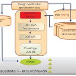
Above picture shows how specifications are extracted from a MAS (Microarchitecture or specification) document and linked to test plan and tests are linked to simulation results. There can be one-to-one, one-to-many or many-to-one relationships. This provides the actual status of verification against the defined objectives. Different views of reports representing the overall status of verification can be obtained from this. Upstream and downstream dependency graphs for each verification objective in the test plan can also be drawn for analysis.

Questa coverage viewer is used to view and analyze the merged simulation result from UCIS database against the goals set for each objective in the test plan. This analysis provides real-time information about the overall coverage along with failing tests (e.g. slew rate in this case) and any coverage holes for which cover points are not implemented (e.g. quiescent current specs in this case). The UCIS data can be analyzed in multiple ways as per individual needs by using command line interface. The bottom part of above example shows failing cover points in ‘red’ color along with their failure counts. By adding user attributes in UCIS, these can be linked to generate debug information. With the progress of the design, effort is put to remove the coverage holes, convert failing tests to pass and improve coverage for design closure. Trend analysis graph of coverage against goal can also be plotted to assess maturity of the design at certain intervals.

Questa SIM – UCIS Framework enables CDV methodology for analog designs (with a few enhancements to existing digital verification flows), thus unifying verification methodology for digital and analog designs. Read this whitepaperwritten by Atul Pandey, Guido Clemens and Marius Sida at Mentor Graphics for more details.

More Articles by Pawan Fangaria…..


Electro-Thermal Simulation of Power Transistors

Electro-Thermal Simulation of Power Transistors
by Daniel Payne on 09-25-2014 at 4:00 pm

Power transistors are commonly used in applications like: hybrid vehicles, electric vehicles, automotive, home appliances, LED lighting, TVs, power and energy. In the old days an engineering team could build their device with power transistors, then after production run some thermal testing to see if they guessed the proper junction temperature, which in turn effects performance like current drive and Rdon. That approach of build first, measure later leads to product iterations costing time and money. There is a better way today, and it involves simulating the electro-thermal behavior prior to tape-out, while still in the design phase when you have engineering options to improve thermal performance.Related: EDA for Power Management ICs at DAC

One of the challenges for IC designs in general is that as you turn the power supply on then current begins to flow in the transistors, and this current heats up the transistor which then changes the electrical performance of the device. Hot-spots on an IC will decrease the current flow in transistors in that local region. It’s not really accurate to assume that the entire die is at a constant temperature across all dynamic input conditions any more.


Temperature in Top-down, cross-cut view

I followed up with Dundar Dumlugol of Magwelby phone to get more details about their approach to modeling heat flow across chip and package for power devices. They’ve been offering an EDA tool called PTM-ET (Power Transistor Modeler, Electro-Thermal) for the past two years that answers engineering questions like:

  • What is the Temperature across my chip?
  • How does heat flow as a function of time?
  • Where should I place thermal sensors in my IC layout?
  • Will my device have thermal runaway?
  • What are the IR drops in my layout?
  • How does changing my package affect temperature?

How Electro-Thermal Simulation Works
The PTM-ET tool first reads in your IC layout as a GDS II or OpenAccess file, along with a technology file provided by the foundry. Using a 3D solver the simulator can calculate the dynamic currents and Joule self-heating in metal and active area. Active devices are modeled based on SPICE results and internally saved as table models for faster simulation speed. All of the electrical and thermal equations are solved self-consistently by using non-linear, iterative techniques.

With this approach you can model heat conduction through metal interconnect, the substrate, lead frame, clips, bond wires, package and PCB.Related: Ensuring ESD Integrity

Accuracy
With any type of simulation it’s natural to ask how accurate the predicted results are compared with measurements. Results presented at the Therminic 2013 conference show good correlation between simulated and measure results of temperature as a function of time:

These simulated results are within a few percent of measured data, which is accurate enough to make engineering decisions like: changing the IC layout, choosing a different package, making new pad placements, adding contacts, or moving the thermal sensors.

Results
A customer designed a display driver circuit, and the PTM-ET tool then simulated their circuit by creating 250K mesh nodes. To perform 0.5ms of transient simulation required just 10 minutes of CPU time and the simulated results were within 5% of measured values.


Temperature in cross-section Metal and substrate

Another customer design was a power management IC with 23 heat sources, and included the package thermal model. Input for a dynamic Electro-Thermal (ET) simulation came from SPICE and the simulation required under 1 hour of CPU time to cover 2ms of time. A static ET simulation took just 10 minutes of CPU time, using about 1M mesh nodes.


Chip-level ET simulation results

Summary
IC engineers designing circuits with power transistors now have a methodology to simulate and analyze the electro-thermal characteristics prior to tape-out. Using such an approach as this will reduce the number of silicon spins required to meet specifications, and confirm that you’ve selected the right package and IC layout to mitigate thermal issues.


TSMC Delivers First FinFET ARM Based SoC!

TSMC Delivers First FinFET ARM Based SoC!
by Daniel Nenni on 09-25-2014 at 9:00 am

Right on cue, TSMC announces 16nm FinFET production silicon. I believe this is the original version of FinFET versus 16FF+ which is due out in 1H 2015. I will confirm this next week at the TSMC OIP event in San Jose, absolutely. Either way this is excellent news for the fabless semiconductor ecosystem and I look forward to the first tear down of a TSMC FinFET SoC in comparison to an Intel FinFET SoC. TSMC 20nm compared quite favorably against Intel 14nm in regards to density and 16FF will do even better.

Let’s not forget that The Chairman (TSMC’s Dr. Morris Chang) speculated that TSMC would not win a majority FinFET market share in 2015. To me this was a head fake to rally the troops. Morris has done this before on conference calls, he is a very clever man. As I mentioned previously, I have never seen TSMC more energized during my last Taiwan trip. Hschinsu on a whole was really buzzing with activity and it was all about FinFETs no matter where I went.

HSINCHU, Taiwan, R.O.C., Sept. 25, 2014 /PRNewswire/ — TSMC (TWSE: 2330, NYSE: TSM) today announced that its collaboration with HiSilicon Technologies Co, Ltd. has successfully produced the foundry segment’s first fully functional ARM-based networking processor with FinFET technology. This milestone is a strong testimonial to deep collaboration between the two companies and TSMC’s commitment to providing industry-leading technology to meet the increasing customer demand for the next generation of high-performance, energy-efficient devices.

For those of you who don’t know, HiSilicon is the ASIC design division of communications giant Huawei. I first encountered HiSilicon in 2008 during an IP licensing negotiation involving SMIC. More recently I visited the new HiSilicon design center in Taiwan. You will be hard pressed to find a leading SoC company without a design center near Hsinchu so they can seamlessly integrate with TSMC. HiSilicon has 100+ people there now and I’m told they are still hiring.

“Our FinFET R&D goes back over a decade and we are pleased to see the tremendous efforts resulted in this achievement,” said TSMC President and Co-CEO, Dr. Mark Liu. “We are confident in our abilities to maximize the technology’s capabilities and bring results that match our long track record of foundry leadership in advanced technology nodes.”

The other interesting thing about this design is that it uses 3D IC packaging combining 28nm mixed signal and 16nm logic chips. TSMC calls this CoWoS (Chip-On-Wafer-On-Substrate) which allows you to integrate multiple chips into a single device. We have written aboutCOWOS many times before and this is an excellent example. To save time and minimize cost you can integrate 28nm blocks with leading edge CPUs for your SoC.

“We are delighted to see TSMC’s FinFET technology and CoWoS[SUP]®[/SUP]solution successfully bringing our innovative designs to working silicon,” said HiSilicon President Teresa He.”This industry’s first 32-core ARM Cortex-A57 processor we developed for next-generation wireless communications and routers is based on the ARMv8 architecture with processing speeds of up to 2.6GHz. This networking processor’s performance increases by three fold compared with its previous generation. Such a highly competitive product can support virtualization, SDN and NFV applications for next-generation base stations, routers and other networking equipment, and meet our time-to-market goals.”

Congratulations to TSMC, HiSilicon, and the entire fabless semiconductor ecosystem for this incredible achievement. And for those who predicted that fabless FinFET chips would “Happen in 2016 at the earliest or never at all”… There are no words left for you.

Also Read: Intel’s 35% Density Advantage Claim Explored

More Articles by Daniel Nenni…..


Atmel Expands Wireless Portfolio

Atmel Expands Wireless Portfolio
by Paul McLellan on 09-25-2014 at 7:00 am

Recently someone described the Internet of Things (IoT) as being the semiconductor classification that we used to call ‘other’. It’s a nice line but actually I think IoT really is something different from what we were already doing before. Although it is a market that cuts across medical, automotive, home-electronics, wearables and more, there really is a lot of commonality, the biggest one being connectivity. It really isn’t IoT if it isn’t, directly or indirectly, connected to the internet.

One company that is well positioned to ride the IoT wave is Atmel. They have a very broad range of microcontrollers at different power/price/performance points along with a number of connectivity solutions. Earlier this week they announced a new set of Wi-Fi SoCs and modules as part of its SmartConnect wireless portfolio. There are two new turnkey SoCs (WILC1000 and WINC1500) and four new modules featuring the SoCs.

The WINC1000 is an IEEE 802.11b/g/n network controller. The WILC100 is an IEEE 802.11b/g/n IoT link controller. These SoCs came to Atmel in the acquisition in July of New Port Media (NMI) and they have been seamlessly integrated in just two months.

Expanding on Atmel’s Wi-Fi offering, the WILC1000 and WINC1500 are SoC solutions optimized for battery-powered IoT applications. These wireless SoCs feature fully integrated power amplifiers for the industry’s best communication range, without compromising cost or performance. Both the WILC1000 and WINC1500 are add-on solutions which can connect to any Atmel MCU or eMPU targeting a wide range of Internet of Things (IoT), consumer and industrial applications. Both products are available either as fully-certified modules ready for production to accelerate a designer’s time-to-market or as discrete SoCs for customers requiring the highest design flexibility.

The WILC1000 and WINC1500 provide multiple peripheral interfaces including UART, SPI, SDIO and I2C. The only external clock source needed is a high-speed crystal or oscillator with a wide variety of reference clock frequencies supported (between 12 – 50 MHz) and are IEEE 802.11 b/g/n, RF, baseband, MAC certified. The WILC1000 is available now as a chip and three different modules. The WINC1500 is available now as a chip and a module, with an evaluation kit, featuring Atmel’s SAMD21 MCU.


More articles by Paul McLellan…


Strategic Materials Conference

Strategic Materials Conference
by Paul McLellan on 09-24-2014 at 8:00 pm

SEMI’s Strategic Materials Conference is coming up fast, on September 30th and October 1st next week at the Biltmore in Santa Clara. This year’s theme, Materials Matter—Enabling the Future of IC Fabrication and Packaging, will take a broad look at what is driving the demand for new materials, and how material suppliers are being impacted by the value chain they serve.

The semiconductor industry has reached a major inflection point: no longer is device scaling and performance driven solely by reductions in feature size. Higher device performance using less power requires the incorporation of many new materials to maintain the industry’s cadence. These material needs to span across the spectrum from fabricating 3D transistor structures, to accelerating interconnect speeds, to packaging the devices in the appropriate form factors for use in phones, tablets and devices encompassing the internet of things. SMC will discuss market opportunities and examine how to win in this “Age of Materials”.

The two keynote speakers are from the biggest IDM and the biggest fabless semiconductor company: Intel and Qualcomm. Matt Nowak of Qualcomm gives the opening keynote on Materials Innovation for the Digital 6th Sense Era. On Wednesday morning, the keynote is delivered by Tim Hendry of Intel on Strategies and New Models for Creating an Affordable Material Supply Chain.

New this year are:

  • Device Makers Session: Materials Challenges for Emerging Technology and Devices
  • Market Trends Session: Economic/Material Trends/Emerging Technology Trends

There are also sessions (with multiple presentations) on Supply Change Challenges, Advanced Memories, Advanced Packaging/TSVs and “beyond 10nm”, the Material Manufacturers Perspective.

The complete agenda for the conference is here. The conference is almost sold out so online registration has been closed. Call Lin Tso at 408 943-7920 for availability if you want to go.


More articles by Paul McLellan…


The Must Read FPGA Book – Secrets Inside

The Must Read FPGA Book – Secrets Inside
by Luke Miller on 09-24-2014 at 1:00 pm

Crockett, Elliot, Enderwitz & Stewart is not a law firm, thank goodness… what you’ll find is that these folks are the authors of the world famous book entitled, now hold on here for a title, this is a creative one “The Zynq Book”, It is free, get your download here. Every designer should have this book no matter what FPGA parts they use. There is also a FREE companion “The Zynq Book Tutorials” when you get to the download page.

Zynq hands down is the most influential FPGA SoC of ALL time. The Zynq Book is already on Amazon’s Top 10 Best Seller list. That really is impressive. Why, because Xilinx SoC is for real and is opening new realms for FPGA design all over the world. A quick Chapter list is below:

CHAPTER 1 Introduction
CHAPTER 2 The Zynq Device (“What is it?”)
CHAPTER 3 Designing with Zynq (“How do I work with it?”)
CHAPTER 4 Device Comparisons (“Why do I need Zynq?”)
CHAPTER 5 Applications and Opportunities (“What can I do with it?”)
CHAPTER 6 The ZedBoard
CHAPTER 7 Education, Research and Training
CHAPTER 8 First Designs on Zynq
CHAPTER 9 Embedded Systems and FPGAs
CHAPTER 10 Zynq System-on-Chip Design Overview
CHAPTER 11 Zynq System-on-Chip Development
CHAPTER 12 Next Steps in Zynq SoC Design
CHAPTER 13 IP Block Design
CHAPTER 14 Spotlight on High-Level Synthesis
CHAPTER 15 Vivado HLS: A Closer Look
CHAPTER 16 Designing With Vivado High Level Synthesis
CHAPTER 17 IP Creation
CHAPTER 18 IP Reuse and Integration
CHAPTER 19 AXI Interfacing
CHAPTER 20 Adventures with IP Integrator
CHAPTER 21 Introduction to Operating Systems on Zynq
CHAPTER 22 Linux: An Overview
CHAPTER 23 The Linux Kernel
CHAPTER 24 Linux Booting

And for all of you Dummies Altera also has an ebook out which you can download HERE.

Ok, like any great product the idea and or the concept gets copied. Do not fall into the FPGA marketing hype. Xilinx has skipped the 20nm Zynq and will have a part that will blow your mind at 16nm, blogs coming soon. Why the node skip? Zynq at 28nm will cover your needs and as I said in an earlier blog, the competition at 20nm is not good. Simply adding in an ARM and calling it a SoC is not going to cut it. The point is, Xilinx executes near flawlessly which is proven today by shipping the 20nm UltraScale ahead of all competitors using the same fab (level playing field).

Also, do not fall into the marketing trap that you need hard floating point, why if soft gets you what you need without the sacrifice of fixed point? If you use the Arria 10, you will lose 5 TMACs of performance when compared with the Xilinx KU115. Yes, you may get 1.5 TFLOPs from Arria10, and 1.3 TFLOPS from Xilinx at 20nm, but are you willing to give up 5 TMACS for that 0.2 TFLOP advantage? The Xilinx KU115 will give you roughly 8.5 TMACS, while the Arria10 comes along with about 3.5 TMACS. Any engineer knows that is not a good deal, especially at least in my realm there is about an 80% fixed point arithmetic to 20% float.

The other marketing angle for the hard float is to appeal to the engineer to say that quantization analysis is just so complicated and hard, so just float your whole design. I frankly find that almost offensive and talking down to the world’s best designers of systems. Do marketing people really think that world class engineers do not know how to design systems? Try floating a CIC filter… Yikes. Bottom line, Floating point is not free and it will cost you in performance, hard or soft.

Not only does Xilinx have the silicon advantage, but the best tools to program using a higher level language. Altera can hype all they want about their OpenCL solution, the proof will be in the pudding, and one will see that Xilinx’s OpenCL solution will in fact be many times better. Chapter 15, Vivado HLS is my favorite chapter. I will keep saying this but Vivado HLS is simply the tool of the decade and will only keep getting better. Xilinx acquiring AutoESL to buy Autopilot was simply genius. All the blogs, PowerPoint, videos may not convince you but try the tool, and you will not be disappointed, especially if you are a VHDL/Verilog code monkey like me. Enjoy the free book and show the world what your Zynq can do!


Explaining HAPS-DX in an elevator

Explaining HAPS-DX in an elevator
by Don Dingee on 09-24-2014 at 7:00 am

Every development team has been through this challenge: finding a tool that looks fantastic, then heading off to the manager one or two levels up who has enough signature authority for the purchase order. Signatures for amounts reading more than a couple of trailing zeros on POs are rarely free, or painless. Continue reading “Explaining HAPS-DX in an elevator”


AMD Design IP Deal with Virage Logic… Oops… Synopsys

AMD Design IP Deal with Virage Logic… Oops… Synopsys
by Eric Esteve on 09-23-2014 at 9:59 am

Whoever has said that history never repeats itself should read this recent PR from AMD! The news can be summarized in three points:

  • Multi-year agreement gives AMD access to a range of Synopsys design IP including interface, memory compiler, logic library and analog IP for advanced FinFET process nodes
  • Synopsys acquires rights to AMD’s interface and foundation IP, and hires a team of engineers from AMD with IP R&D expertise
  • These agreements enable AMD to realize ongoing engineering efficiencies and focus engineering efforts on product differentiation

The deal content is in these first two points: AMD can get access to the most expensive IP from Synopsys, because designed for advanced FinFET process nodes, in exchange, Synopsys will hire a team of IP expert engineers from AMD, and get rights for existing AMD’s interface and foundation IP. By the way, FinFET is such a wonderful process that the extra cost for IP compared with bulk is not negligible as I have heard about 1/3[SUP]rd[/SUP] more…

This deal is very similar with a previous deal between AMD and Virage Logic in 2008, when the IP vendor was paid by AMD with rights to PCI Express, USB or SATA IP instead of cash to compensate the memory compiler and logic libraries. Thanks to this deal, Virage Logic had entered into Interface IP market, 18 months before to be acquired by Synopsys for $315 million in cash. No design team was involved in the 2008 deal, but this came less than one year later, when “NXP transfer over 160 employees and the assets associated with selected advanced CMOS libraries, IP blocks and SoC architecture along with other classes of semiconductor IP”. In both cases, these deals have helped Virage Logic to quickly develop their IP port-folio, in particular by including Interface IP.


The above picture, extracted from the “Interface IP Survey” last version (Release 6), has been specifically designed for Semiwiki and Linkedin readers. This is a graphic view of the ASIC and ASSP design start for HDMI, SATA, PCIe, USB 2, USB 3.0, Ethernet, MIPI and DDRn memory Controller IP. If you look at a form (between a circle to an ellipse), the “diameter” (the larger lenght) is proportional to the total number of design starts including such IP function, internally developed or acquired from an IP vendor. In the real life, some SoC may integrate several IP, so the forms may recover each other. For example, we know that an Application Processor SoC may integrate MIPI, HDMI, USB 3.0 and LPDDRn. On the other hand, some of these interfaces are not supposed to be integrated in the same ASIC/ASSP, like Ethernet and MIPI, so the forms are not recovering. SATA is an exception: there are too few design starts, so the form is small and can’t recover with every protocol it should, and MIPI & PCIe should recover a little bit, but the forms are too far. That’s the model limitations, but the picture gives a good view of the respective adoption rate of the various protocols.

The largest by far is (LP)DDRn. If you agree with the System-on-Chip definition, an “IC integrating a Processor (CPU or GPU) core”, you realize that about 100% of the SoC will integrate a memory controller. The more intuitive definition linked to the word “system” suggests that a SoC will be at the hearth of an electronic system, so the chip is expected to “interface” with other IC and with the outside world. That’s the reason why the DDRn form is not only the largest but this recovering with most of the other forms, representing the interface protocols.

From a business point of view, we have shown in a previous post that these interface protocols have exhibited a very strong growth during the past 5 years, and are expected to grow again during the next 5 years. That’s why the rights for interface IP from AMD had a great value 5 years ago for Virage Logic and today for Synopsys. I should have a more precise figure in the next few days, but I suspect the IP business generated with the above mentioned protocols to reach between $900 million to $1 billion by 2020…

When traditional EDA business is almost flat since many years, you better understand why the interface IP “cake” can attract Synopsys and Cadence, and also why these two companies are heavy investors. I don’t think only about the acquisitions that both companies have done during the last three or four years. As a matter of fact, each of them is building a large engineering team, if I mention 1,300 engineers, only dedicated to Design IP for Synopsys, I am probably below the real number as of today (certainly in fact, as this number does not take into account the above mentioned team from AMD). I guess that we can expect to soon get IP related news from Cadence…

You may find additional information here and the Table of Content for “Interface IP Survey 2010-2013 – Forecast 2014-2020” will be available soon (you may contact me through Linkedin if you want to receive it as soon as it will be completed).

Eric Esteve from IPNEST


The TSMC iPhone 6!

The TSMC iPhone 6!
by Daniel Nenni on 09-23-2014 at 7:00 am

Fortunately Paul McLellan and I missed IDF. Paul was atop Mt. Kilimanjaro and I was in Taiwan signing books. After reviewing the materials and watching the videos we really didn’t miss much in regards to mobile so no regrets. The Apple event would have been fun even though I won’t be buying an iPhone6 or an iWatch and I will tell you why.

In case you missed it, the first iPhone 6 tear down is up on iFixit and surprise-surprise it is filled with silicon from TSMC’s customers (Apple A8, Qualcomm: modem, PM IC – RF transiever – LTE receive and envelope tracking, Murata wifi module, Broadcom touchscreen controller, NXP NFC, and chips from Skyworks, InvenSense, Avago and TriQuint). The absence of Samsung silicon was not a surprise however and it supports my theory that, given the choice, fabless companies will partner with pure-play over IDM foundries, absolutely. The fact that Samsung and Apple have intellectual property issues and Samsung has constant anti Apple advertisements probably does not help either but that comes with competing with your customers I suppose.

Also Read: Intel Core M vs Apple A8!

14nm may be a different story. Intel 14nm did not fit Apple’s requirements so they must choose between TSMC and Samsung or more than likely use a combination of both. 10nm will also be a different story as I have seen the Intel Foundry people at Apple and have heard tales of them aggressively pushing 10nm foundry services. Unfortunately, Intel corporate is still saying they have a 2-3 year lead on 10nm over the foundries and a 45% density advantage which is not true at all. As I mentioned before, the foundries are on schedule for 10nm product tape-outs in Q4 2015. Intel may have 10nm silicon out by then but I highly doubt it will be from foundry customers and the claimed 45% density advantage at 10nm is absolute nonsense. This goes against Intel’s credibility and trust is a significant factor when fabless companies choose a foundry partner, believe it.

Today, Intel Custom Foundry is suffering the same challenge as Samsung Foundry. Other groups within these companies are pissing off the fabless semiconductor ecosystem. This same thing happened at the start of the fabless revolution. The first fabless companies rented space from IDMs but when they started to need more fab space or once they started competing with the IDMs the relationship soured. As a result, the pure-play foundry model became dominant and the rest is history.

In regards to the iPhone6, I find it funny that we worked so hard to make things smaller and now they are getting bigger! I don’t wear a watch so unless the iWatch does something truly amazing I don’t want the additional interrupts. The problem I have with the iPhone6 is the processor speed. I expected the dual cores to clock in at 2GHz versus the paltry 1.4GHZ. The A6 is 1.3GHz, the A7 is 1.3GHz, and the A8 is 1.4GHz. The A7 jumped from 32 to 64-bit so I can understand the comparable GHz but what is the A8’s excuse?

I think I know but I would like to hear your theories in the comment section before I share mine.


Really Apple? Tanazania Leads US in Mobile Payments

Really Apple? Tanazania Leads US in Mobile Payments
by Paul McLellan on 09-23-2014 at 1:00 am

I was in Tanzania a few weeks ago. One of the conceits that we have in the US is that we lead the world in technology. That is true in many areas but in mobile the US is a laggard. Just look at the fuss made about NFC payments in the new iPhone given that Japan had mobile payments over a decade ago.

Another area where the US is a laggard, or maybe it is the same area, is the capability to move money around by phone. In rough numbers, the world has only 2B bank accounts, 1B credit cards but 7B mobile phones. If you were starting from scratch you wouldn’t base a payment system on giving every customer cards and giving every merchant a reader, you would find a way to leverage the mobiles that everyone already has.

The area where this is most advanced is the area where banking is least advanced so there is not really any infrastructure to compete with. That is the M-Pesa system (pesa is the swahili for money) first introduced in Kenya and then in Tanzania. Driving around in Tanzania there were M-Pesa signs everywhere. Every bar, every little store, even little tents set up at the side of the road. M-Pesa was launched in 2007 by Vodafone subsidiaries.


How successful is M-Pesa? In a nice coincidence the Economist published just the table that I needed over the weekend. In Kenya, there are more accounts than there are people. In Tanzania there are only about 420 accounts per 1000 people but the value of all the transactions is a staggering 65% of GDP. It is “only” 55% in Kenya with even greater penetration. It is even 18% in Afghanistan (where it is called Roshan but it is still run by Vodafone).

People use M-Pesa for all sorts of things but one thing is that children working in cities can easily transfer money back to the villages where their parents live. In the past, since there were banks only in the city, there was no way to do this other than getting on a bus for what might be a very long round trip. The child goes to an M-Pesa store and pays the money in to transfer it to his or her own phone account. Then they transfer it to the parents account using the cellphone network. The parent goes to an M-Pesa store, shows the code on the phone and collects the cash.

Another area where US centric opinion tends to underestimate things is the size of internet and mobile businesses in China. For instance, China Mobile has over 750M subscribers. So that is not just twice the entire US population, it means that it is almost 3 times as big as the US carriers (AT&T, Verizon, T-Mobil, Sprint etc) put together. They plan to put in about 500,000 LTE base stations in the next few years. The scale is amazing.

How about internet commerce? Amazon is the world leader, right? Not even close. Since Alibaba just went public in New York last week you might already have seen this, but Alibaba is over twice times Amazon’s size, with $269B versus Amazon’s $116B. They do an astounding $9,368 per second of business. I sometimes like to point out that a modern semiconductor fab depreciates at around $20/second but this is a couple of orders of magnitude larger.


There was lots of noise when WhatsApp was purchased by Facebook. In China, the equivalent service is called WeChat (you can use it in the US too but it is mostly people who know someone in China who seem to). It makes far more money per person than WattsApp (although it has fewer subscribers but is growing exponentially).

So don’t assume the US leads in everything unless you actually know the facts.


More articles by Paul McLellan…