webinar IPXACT banner

Samsung 14nm FinFET Design with Cadence Tools

Samsung 14nm FinFET Design with Cadence Tools
by Daniel Payne on 09-22-2014 at 5:30 pm

The first consumer products with 20nm processing are arriving in 2014 like the 2 billion transistor A8 chip in the iPhone 6, however at the 14nm node there are new designs underway to continue the trend of Moore’s Law. To get a better feel for the challenges of designing with 14nm FinFET technology I watched a 23 minute video presentation by Dr. K.K. Lin of Samsung over at the Cadence site. I prefer listening to real EDA tool users instead of vendor presentations, because I get to learn their methodology and the benefits compared to previous approaches.

Related: What Apple Talked about on 9/9/2014

Samsung decided to create two versions of 14nm FinFET: 14LPE (early version) and 14LPP (lower power). You can start prototypes now and expect production by end of 2014. Other foundries have re-used much of their 20nm planar technology into 14nm FinFET, resulting in little size reduction whereas Samsung has an aggressive 78nm poly pitch that enables about 10% smaller areas. Performance improves up to 20% and power is reduced by 35% when going from 20nm planar to 14nm FinFET with Samsung. Cadence users have complete PDKs (Process Design Kits) available now.

Related: A Deeper Insight into Quantus QRC Extraction Solution

The Virtuoso tools from Cadence enable 14nm design using the IC12 tech file with features like:

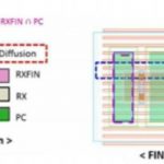
Pcells provide layout automation of FinFET transistors by adding FIN dummy above and below the device, plus quantized fingers:

Layout cell instances can be abutted to avoid any of the complex violations found in 14nm. DPT started at the 20nm node and continues at 14nm, so with Virtuoso you can interactively view any of the DPT issues like: coloring loop detection, color shorts and DPT DRC errors.


For custom IC designs you can perform interactive routing with a Virtuosofeature called pin to trunk (P2T), and designers at Samsung have measured turn-around time improvements between 14% and 63% on: source/drain routing, gate routing and general routing. The new Virtuoso space-based router (VSR) used on 14nm can improve routing productivity by up to 75%.

Related: What’s New with Circuit Simulation for Cadence at DAC

The impact of LDE issues is reduced in Virtuoso by an architecture that enables quick iterations between layout and simulation, even before the design is LVS clean. Using three automation features (Analog Placement, P2T and VSR) provided a 24% schedule reduction compared to older, more manual methods.

Related: Designing an SoC with 16nm FinFET

View the entire 23 minute video here at the Cadence site, and there’s no registration required.


Expansion at Calypto through Real Value Addition in SoC Design

Expansion at Calypto through Real Value Addition in SoC Design
by Pawan Fangaria on 09-22-2014 at 1:00 pm

When we get the notion of expansion of a company, it always provides a positive picture about something good happening to boost that expansion. There can be several reasons for expansion such as merger & acquisition, formation of joint venture or partnership, large customer orders and so on. However, organic expansion which happens due to real value addition into the products that drives customer demand and satisfaction brings eternal cheer and confidence among company’s workforce leading to ever increasing value of the products and the company’s general ecosystem.

These are the thoughts which came to my mind when I met Sanjiv Narayan, VP & Managing Director at Calyptoin its Noida office. Sanjiv has been a good friend of mine since my Cadence days; I admired his knowledge of synthesis, optimization and verification domain. He heads Calypto’s Noida site which has a strong committed workforce of about 60 people; 90% of the workforce is involved in R&D development, that’s quite impressive. Since we had met after a while, we had a long conversation on several aspects; I am summarizing some of the prominent ones below.

Accommodating the current team comfortably and looking forward to further expansion driven by growing adoption of their products, Calypto has already moved (this is the third time in last ten years) to a new facility equipped and ready to accommodate a larger team. The India team provides major R&D support to all product lines of Calypto. Sanjiv expects the new office to be able accommodate an additional 50% growth in headcount and Calypto is already aggressively hiring for R&D and Application Engineering positions in India. Calypto is seeing rising business and increased usage of their tools in Asia Pacific (AP) region. They already set up an office in Korea earlier this year to support Calypto’s Korean customers. The expanded Application Engineering and Services workforce in Noida will support the entire AP region. Calypto is also setting up an office in Bangalore – it should be operational before the end of the year.

So, what’s driving this expansion? Of course, Calypto has a pioneering product portfolio at system and RTL level coupled with the semiconductor industry’s unique formal verification technology; Catapult HLS tool, PowerPro power optimization tool at RTL level and SLEC sequential equivalence checker. What’s unique about them – Catapult can synthesize hardware descriptions written in either C++ or SystemC to RTL, no proprietary or specific standard is needed; PowerPro is reported to provide the best power saving in the industry with functionally clean RTL proven at the gate level; SLEC is the most versatile formal verification tool that can accurately check (through its unique sequential equivalence checking capability) equivalence between C++/SystemC and RTL (SLEC HLS) and RTL and optimized RTL (SLEC RTL and SLEC Pro) which may be obtained either manually or through the use of PowerPro.

Naturally, Calypto is gaining customers’ attention, increasing customer base and seeing consistent growth in its revenue over the years with top semiconductor companies using their products. To know more about their products/technologies and general technical learning, attend some of the upcoming events where Calypto is presenting –

Sep 25, 4:00 PM – 5:30 PM atDVCon India in Bangalore

Tutorial on “Low Power Design & Verification Using HLS” to be presented by Sanjiv Narayan, Sandeep Dagar, Vikas Tyagi and Vishal Sinha

Oct 1-2, 11 AM – 6 PM atARMTechCon in Santa Clara Convention Center, CA

Exhibit at Booth #715

Also read:
Accelerating SoC Verification Through HLS
How to Reduce Maximum Power at RTL Stage
Designing the Right Architecture Using HLS

More Articles by Pawan Fangaria…..


Is Number of Signoff Corners an Issue?

Is Number of Signoff Corners an Issue?
by Daniel Nenni on 09-22-2014 at 12:00 am

Semiconductor companies continue to use the traditional corner-based signoff approach that has been developed more than 40+ years ago and has since remained mainly unchanged as an industry paradigm. Initially it had 2 corners, namely Worst Case (WC) and Best Case (BC) with the maximum and minimum cell delay respectively. Note that wire and via delays were negligible. Later, the number of corners increased to 4 and after that it has been growing exponentially, especially during last 10-15 years. Figure below illustrates the spread of timing signoff corners used in different design companies.

Number of timing signoff corners
One can see that the number of corners grows exponentially with increase of variation sources for each new technology node. Some people believe that it is possible to reduce corners, but it may be risky to remove any so-called “redundant” (or dominated, or less important, etc.) corners. For example, {SS-process + Fast-Metal} is needed for the setup check, because a violation may happen in a path where launch and data paths are cell-delay dominated and capture is metal-delay dominated. So, using only {SS-process + Slow-Metal} may lead to missing violations. Some companies also ignore a need for more corners to take into account Aging Degradation (AD), multi-voltage non-correlated or partially correlated domains (supplies), the temperature inversion, other effects (like the NTBI, Hot electron injection, etc.), FinFet, DPT (Double Pattern Technology), LSE (Layout Dependent Effects), etc., which may produce the extreme delays in some intermediate points.

Even with so many corners, there is no guarantee that we do not miss some violations due to non-linearity (like the cell delay vs. voltage) and even a non-monotonic behavior (like the temperature-inversion) for some variation-factors, and because of a non-perfectness of conventional tools and derating methods, and ignoring some physical phenomena like correlations. Also, we will need to add at least two more points for Aging Degradation (AD): the BOL (Begging-Of-Life) and the EOL (End-Of-Life).

Note that one can doubt if we really need to run BOL and EOL at all the PVT corners and is it fair to multiply all corners by 2. The answer is “yes ” and an explanation is similar to already used for some other variation-factors—most corners may not need to be run for BOL and EOL for typical paths, but there may be special not typical path structures (with cell- or net-delay dominations in different sub-paths) that need not “typical” age model. Let’s consider one example for hold check. A common mistake: There is no need for using SS library & EOL model, because all cell delays become slower. In reality, for some rare path structures, SS & EOL model is needed, because a violation may occur in a path where the launch and data paths are metal-delay dominated and the capture is cell-delay dominated.

Actually, even more corners may be needed because there is a need to add vias corners (or via RC-models) that are similar to the current wire RC models. Vias delays have become significant and are not correlated with RC-wire models. Example: the worst-case situation (corresponding to the minimum setup slack) is when the RC-worst model is used for wires and the RC-best model is used for vias. The capture path has big via delays with almost no wire delays; and cell delays are irrelevant here. Adding via models will increase the corner number by 4-5x.

Using so many PVT/RC/Via corners (>1000) may be not acceptable from the design time and costs considerations. Also, the number of signoff scenarios is a product of corners and modes (functional, test, etc.) and may become too big to be handled by the IC Compiler (ICC) or PrimeTime (PT) or other similar tools. Additionally, designers need to perform 10-30 ECO iterations for all those scenarios to close timing. The runtime has become a serious issue and may be a work-stop for emerging technologies.

Thus, the question is: Is the corner-based signoff and corner number becoming a serious problem?

More Articles by Daniel Nenni…..


Xilinx UltraScale leads the way on connectivity

Xilinx UltraScale leads the way on connectivity
by Luke Miller on 09-21-2014 at 10:00 am

Even though Xilinx FPGAs seem to keep growing in densities and gobbling up boards into a single part, there is still the need for chip to chip connectivity and of course backplane connectivity. Xilinx 20nm UltraScale, TODAY, can really move 28 gb/s over the back plane. This is something that you cannot do with Altera 20nm, they are limited to 17 gb/s for the backplane. Arria Chip-Chip they are behind as well, only at 28 gb/s. Xilinx 20nm UltraScale will get you at 33 gb/s chip to chip. Higher data rate means less lanes to do more.

Need some proof, please watch this video seeing REAL Xilinx UltraScale hardware working, and is available now. Also demonstrates that Xilinx is the leader in 400G/500G solutions as well. This is a great video and is really well done.

Now Altera will say Arria is midrange, wait for the Stratix-10. That is an interesting scenario. Do you know how hard it is to manage a family/product with one fab? Xilinx is the leader in execution, and it requires vast amount of engineering resources. So say you do end up designing in an Arria 10, do you think you are going to get the engineering support when the smooth Intel 14nm process starts to crank out wafer’s for Altera? Has Altera doubled its engineering resources? Both used the 20nm TMSC fab, Xilinx is faster and denser. What happened to Arria? Same process, why is DSP limited to 550 MHz and Xilinx 741 MHz? It is all about engineering and architecture.

The Xilinx Gigabit Transceivers are unleashing what I would call nothing short of a revolution. High speed serial is here to stay and JESD204b and Hybrid Memory Cube are absolutely tremendous. Of course Xilinx leads the way with these technologies. Here is an excellent video of the World’s first Hybrid Memory Cube 15G using an Xilinx UltraScale design. Please watch and enjoy, once again technology that is available here today.

For some of you, and that is many that still need DDR4, Xilinx UltraScale still does that, and is the world’s fastest and best in DDR3/4 solutions, not in simulation or in tools but in REAL silicon!

For more video’s on Xilinx UltraScale I encourage you to check out this link and really spend the time to clearly understand the advantages Xilinx has over Altera. And may I ask you, why are you using Altera? Wait till I get to write about 16nm, my oh my…


TCAD to SPICE

TCAD to SPICE
by admin on 09-21-2014 at 7:00 am

Power devices have historically been made from silicon (Si), which has reached the limit of electric power loss reduction. With the superior physical and electrical properties of silicon carbide (SiC), we can expect to see a significant expansion in the amount of electric power conversion of electrical equipment as well as reduced loss during conversion. One of the big steps in bridging the TCAD and design worlds is the capability to define the process in the TCAD environment and end up with SPICE models that allow designers to simulate the capabilities..

Next Tuesday, September 23rd, Silvaco have webinar TCAD to Spice Simulation of SiC and Si Power Devices. The webinar is from 10-11am Pacific time and is presented by Dr. Eric Guichard, who is Silvaco’s Vice President of the TCAD Division. He is responsible for all aspects of TCAD from R&D to field operations. Since joining Silvaco in 1995, he has held numerous positions including director of Silvaco France and most recently Director of Worldwide TCAD Field Operations. Dr. Guichard holds an MS in material science and a PhD in semiconductor physics from Ecole Nationale Polytechnique de Grenoble, France.

The webinar will provide a discussion of the methods used to design, simulate and optimize the performance of power devices using TCAD and SPICE simulations. Silicon has long been the semiconductor of choice for high-voltage power electronics applications. However, wide-bandgap semiconductors such as SiC have begun to attract attention due to their projected improved performance over silicon. Simulating SiC devices is more challenging relative to silicon-based devices. In this webinar Eric will review the requirements to accurately simulate SiC-based power devices. He will also present a completely automated TCAD to SPICE flow that helps reduce the cost and time taken to develop a Silicon-based IGBT power device.


What attendees will learn:

  • Key challenges of power device TCAD simulation
  • Key challenges of SiC TCAD simulation
  • TCAD simulation of SiC IGBT (Insulated gate biplolar transistor), Trench MOS and DMOS
    • 2D and 3D TCAD simulations (meshing, solver, physical models)
    • When to use 3D over 2D
  • Full TCAD to SPICE IGBT flow example
    • Process and Device simulations for IV curve generation
    • TCAD-based SPICE parameter extraction using HiSIM-IGBT compact model
    • Correlation between circuit performance and process variation
    • Circuit performance optimization

More details on the webinar including a registration link are here. If you cannot make this date and time then register anyway, you will get sent a replay link to the webinar soon afterwards.

More articles by Paul McLellan…


Intel’s 35% Density Advantage Claim Explored

Intel’s 35% Density Advantage Claim Explored
by Daniel Nenni on 09-20-2014 at 1:00 pm

The previous blog I did on the density difference between Intel 14nm and TSMC 20nm caused quite a stir and many interesting comments which I would like to address. After writing thousands of blogs on a wide variety of topics I have found that playing the devil’s advocate stimulates the most productive conversations and in this case it proved to be true. The Intel Core M vs Apple A8! blog went viral last week and resulted in some very interesting points made in the comment section that I feel should be explored in greater detail.

First is how we measure density. The semiconductor industry is all about packing more transistors in a smaller space. It is part of Moore’s Law, it is how we get less expensive consumer electronics, it is a badge of honor really. There are two transistor numbers you can use: the number of transistors in a design schematic and the number of transistors in the final layout which is then manufactured. The difference between these numbers varies but after taking a quick poll amongst leading edge design and layout people the range is 0-10% more transistors in the layout. Since density is a badge of honor most companies use the layout transistor count but if it serves a marketing purpose they will use the schematic transistor count. Either way, considering the point I’m trying to make, it doesn’t really matter.

Second, comparing the Intel Core M processor and the Apple A8 SoC is like comparing an orange to an apple but this is the only data we have today and it is a good starting point for a density discussion. The architectures are different (CPU vs SoC), the processes are different (20nm planar vs 14nm FinFET), and the companies are very different (IDM versus Fabless).

Third, the performance, power, and functionality of the chips are not part of this discussion. Tear downs and third party benchmarks will be required and they are not available yet. When they are, we can look back on this discussion and see if we were right and if not we can see where we went wrong. All in the interest of science, right?

Here is the argument: Intel claimed a 35% density advantage over TSMC during their November 2103 Investor Meeting using the middle slide above. Intel also used the Altera slide as support for their claim. TSMC rebuffed that claim during a quarterly conference call using the slide on the left.

According to Apple the A8, which is manufactured by TSMC on a 20nm planar process, has about 2B transistors on a 89mm2 die. According to Intel the Core M manufactured on a 14nm FinFET process has about 1.3B transistors on an 82mm2 die.

Given that:

[LIST=1]

  • According to TSMC, 16nmFF+ has a 15% density advantage over 20nm planar
  • We do not know what type of transistor count Intel and Apple uses but assume the worst case with a 10% variance (upsize Intel by 10%)

    Intel’s 35% density advantage claim just does not hold up, not even close. Time will tell, silicon does not lie, but for now TSMC’s density slide is much more honorable than Intel’s. And let’s not forget that Intel’s processes are highly specialized for a single product and TSMC’s processes serve a much wider range of applications. If true, this lack of density gap is really big news for the fabless semiconductor ecosystem, absolutely!

    More Articles by Daniel Nenni…..


  • Who will be “lucky dog” in 4G LTE basebands?

    Who will be “lucky dog” in 4G LTE basebands?
    by Don Dingee on 09-19-2014 at 5:00 pm

    The official term is “beneficiary rule”, but among colorful racing broadcasters, drivers, and fans it is more commonly referred to as the “lucky dog”: the driver who is down a lap, but gets to advance to the lead lap by virtue of being farthest ahead when a caution flag is raised.

    Qualcomm has lapped the entire field when it comes to cellular baseband chipsets, holding 66% market share according to the latest figures from Strategy Analytics. Continue reading “Who will be “lucky dog” in 4G LTE basebands?”


    MEMS+, Bringing MEMS into the Electronic World

    MEMS+, Bringing MEMS into the Electronic World
    by Paul McLellan on 09-19-2014 at 1:59 pm

    One of the things about MEMS devices is that they almost always live on a chip that also contains the electronics necessary to process the output from the sensor. For example, an on-chip accelerometer for a car airbag deployment will contain the electronics necessary to process the signal from the sensor and end up with something much closer to “we’re crashing, deploy the airbags” versus “we’re OK, don’t fire off the airbags.”

    The design of the MEMS devices themselves are typically done with some form of finite-element analysis (FEA), a very general approach to designing mechanical structures. However, these models of the device are very complex and slow to evaluate due to the huge number of degrees of freedom. This is fine for designing the device itself but for working with the electronics a simpler model of the device is required that is accurate enough for the purpose but is also fast to evaluate.

    What is required is a model that can be imported into Mathworks/Simulink or Cadence/Virtuoso and allows the circuits being designed to be evaluated with the MEMS device in place. In effect we want the input to the electrical simulation to be the input to the MEMS device, which is typically mechanical/force/temperature not the electrical signal it produces. So we input deceleration and then can see the signals that the sensor creates, how they are processed all the way up, potentially, to how the software in a microcontroller reacts. Other MEMS devices are more on the output side, such as mechanical switches or DLP mirrors, but the same idea remains. The electronics and the MEMS devices need to be cosimulated with enough accuracy on the MEMS side to ensure that the electronics is designed correctly but without requiring a model with such fidelity that the simulation is prohibitively slow. The traditional approach to doing all this has been to hand-craft a model. To make it possible to even do that, tye model is often over-simplified which can lead to errors slipping through the cracks.


    Coventor’s MEMS+ and other products are the tool of choice for MEMS designers. Over half the top 10, half the top 20 and half the top 30 are Coventor customers. So what is MEMS+? It is a tool for creating high order finite element models that run in MATLAB, Simulink, and Cadence instead of proprietary field solvers. It allows models of MEMS components to be constructed from parametric finite elements such as rigid shapes, flexible shapes, side electrodes, interdigitated combs and more. The basic building blocks of MEMS devices. Then models can automatically be generated for use in MATLAB/Simulink and Cadence. The models include mechanical, electrical and gas damping effects, and are small and fast enough for transient simulations, simulating in minutes on a standard laptop.

    The models are parametric so it is straighforward to vary the design to take account of, for example, manufacturing variability. For example, an interdigitated comb can take account of the thickness of the elements, the height, the sidewall incidence from over-etching etc.


    MEMS+ 5.0 was announced by Coventor recently. The key new features are:

    • Improved Reduced Order Model generation and export
    • Now exports Verilog-A and MATLAB/Simulink models (up to 100X faster than complete nonlinear models )
    • MATLAB/Simulink ROM’s support 3D result visualization
    • New option to include mechanical nonlinearities for frequency hysteresis (Duffing effect) and quadrature
    • Improved model library

      • New comb models for movable flexible structures
      • Improved side electrode and contact models
      • New squeezed film damping models for side electrodes
      • Support for modeling out-of-plane structures such as corrugations
      • New charge output for piezo-electrical layers
      • New generic spring and damper

    The SUN will NOT set on Oracle!

    The SUN will NOT set on Oracle!
    by Daniel Nenni on 09-19-2014 at 7:00 am

    Larry Ellison resigning as CEO of Oracle caught me by surprise. I definitely did not see that one coming. Talk about the end of an era, as a 30+ year Silicon Valley veteran there have been quite a few industry icons that stand out amongst the others: Dave Packard, Bill Hewlett, Gordon Moore, Andy Grove, Bill Gates, Steve Jobs, and Larry Ellison are definitely in my top ten. SUN Microsystems was also one of my favorites since I’m a computer person at heart and they changed the world. So when Larry Ellison rescued SUN from IBM I was ecstatic. Unfortunately the emails I have received today suggest that clouds may be coming to which I totally disagree.

    Early in my career I almost joined SUN but opted for a SUN compatible start-up called Solbourne Computer. Not one of my best ideas. In fact, it was my second worst career decision, joining Avant! being the first. I started my career with the mini-computer and saw a room full of compute power end up on a desktop with the first SUN System. That same compute power is now in a watch by the way. SUN really created the internet in the 1980s and rode the dot-com bubble into oblivion. Larry Ellison bailed SUN out in a $7.4 billion dollar acquisition in 2010 to better position Oracle in the server business against HP/Intel and IBM. Larry Ellison and SUN co-founder Scott McNealy were also good friends so that probably had something to do with it as well.

    Larry is probably the most ego fueled CEOs on my list and I will never forget what he said about cloud computing:

    “The interesting thing about cloud computing is that we’ve redefined cloud computing to include everything that we already do. … The computer industry is the only industry that is more fashion-driven than women’s fashion. Maybe I’m an idiot, but I have no idea what anyone is talking about. What is it? It’s complete gibberish. It’s insane. When is this idiocy going to stop?”

    I feel the same way about the Internet of Things. It’s called embedded IC design and we have been doing it for a lifetime, right?

    I had never really watched America’s Cup until Larry turned it upside down. Now I not only watch the races but my beautiful wife and I attend them whenever possible.

    “I enjoy the competition and the process of learning as we compete. The whole thing is just fascinating. I don’t know what I’ll do when I retire. When I go sailing, I look around … anyone want to race? I just love competing as opposed to just going out and watching the sunset.”

    Not only is Larry ultra competitive, he has no problem writing some very big checks and since the SUN acquisition is on his shoulders I’m confident those checks will continue. Thanks to Larry Ellison, Oracle is now a leading edge fabless semiconductor company and a key collaborator within our ecosystem. If you read the fine print on Larry’s resignation it says he will now lead software and hardware engineering full time without CEO interrupts. I think this is a VERY good thing for the fabless semiconductor industry, absolutely.

    More Articles by Daniel Nenni…..


    MIPI Alliance introduces C-PHY, Synopsys launch C-PHY VIP

    MIPI Alliance introduces C-PHY, Synopsys launch C-PHY VIP
    by Eric Esteve on 09-18-2014 at 12:05 pm

    The set of MIPI PHY specifications has enlarged during last night, as theMIPI Alliance has introduced the new C-PHY spec on September 17th, a physical layer interface for camera and display applications. “The MIPI C-PHY specification was developed to reduce the interface signaling rate to enable a wide range of high-performance and cost-optimized applications, such as very low-cost, low-resolution image sensors; sensors offering up to 60 megapixels; and even 4K display panels,” said Rick Wietfeldt, chair of the MIPI Alliance Technical Steering Group.

    The next day, Synopsys has released a new Native SystemVerilog-based MIPI C-PHY Verification IP to help enable engineers to verify interfaces such as MIPI CSI-2 v1.3, which includes the MIPI C-PHY. The MIPI MIPI C-PHY™ specification uses three-phase digital coding techniques. This means that a chip integrating MIPI C-PHY will use 3 pins to form 1 unidirectional lane (in fact a trio), the clock being embedded. Thus we don’t speak any more about Gb/s (Giga bit per second) but Gsym/s (Giga symbol per second), the symbol being formed by the lane trio. When a differential signaling technique (like for MIPI M-PHY) uses two wires to carry one symbol equal to one bit (minus the encoding, for example with 8b/10b, only 0.8 bit), the MIPI C-PHY will use three wires to carry one symbol equal to 2.28 bits. The benefit is that you reach (about) the same bandwidth with a MIPI C-PHY running at 2.5 Gsym/s on 3 wires than with a MIPI M-PHY running at 5.8 Gb/s on 2 wires. Designing at lower frequency (in this range) is probably easier, and the 2.5 GHz lane should generate less perturbation than the 5.8 GHz… don’t forget that the first application is mobile phone, thus avoiding to perturb RF signals can only be good!

    Synopsys providing the MIPI C-PHY Verification IP the same day the specification is introduced is already great news. But another PR was launched the same day: Synopsys has released the MIPI D-PHY v1.2, running up to 2.5 Gbps per lane, or an aggregated data throughput of up to 20 Gbps for high-resolution imaging applications. According with Synopsys, this new “MIPI D-PHY is 50 percent lower in area and power compared to competitive solutions, reducing silicon cost and extending battery life”. There is also an interesting quote from Sean Mitchell, senior vice president and COO at Movidius, saying that “The DesignWare MIPI D-PHY offered low power consumption, high performance and configurability options that were critical to the success of our Myriad 2 Vision Processing Unit”. If you take a look at Movidius web site, the Myriad 2 Vision Processing Unit targets the following applications:

    • Smartphone / tablet cameras
    • Wearables, action cameras, and electronic eyewear
    • Embedded devices (home automation, industrial, and robotics)

    If using MIPI D-PHY for Smartphone and Media Tablet looks pretty obvious, listing other applications like wearable and embedded devices is very interesting: MIPI technology is going outside of the mobile phone (or tablet) industry! In fact, we expect such information to become more common in the future. The benefits coming with MIPI technology usage like better power/bit efficiency, interoperability or availability of Off-The-Shelf ASSP running in 100’s million units in production (with a positive impact on price) should make MIPI powered IC a very attractive solution for wearable, IoT and embedded devices!


    I was about to miss the latest, but not least, MIPI related PR released the same day by Synopsys: “Leadcore Achieves First-Pass Silicon Success with DesignWare MIPI IP in Smartphone Application Processor SoC”. In fact Leadcore is a chinese Application Processor SoC maker, targeting a market which is probably the most competitive on a world-wide basis today, the Chinese mobile market.

    “With the tight time-to-market windows in the mobile market, we needed an established IP supplier that would provide high-quality and reliable solutions,” said Dijun Liu, vice president, Leadcore Technology. “We successfully integrated the DesignWare MIPI IP into our design within two weeks, letting us focus our efforts on the differentiating portions of our design. The DesignWare IP helped us meet our project schedule and improved our product’s time-to-market. We fulfilled our customer’s requirements by using DesignWare IP from Synopsys.”

    The MIPI specification integrated into Leadcore INNOPOWER LC810 is DesignWare MIPI D-PHY, compliant to the MIPI D-PHY interface specification v1.1, supports up to 1.5 Gbps and is configurable for host or device applications. So, if we summarize, Synopsys has launched Verification IP for MIPI C-PHY, compliant with MIPI CSI-2 v1.3, released the MIPI D-PHY v1.2, running up to 2.5 Gbps per lane, or an aggregated data throughput of up to 20 Gbps, and shared a customer success story, the Leadcore LC810 integrating MIPI D-PHY v1.1… We understand this quote from Joel huloux, chairman of the board of MIPI Alliance, “Over the last 10 years, Synopsys has played an active role in MIPI Alliance working groups, contributing to the development and proliferation of MIPI Alliance technology,” as Synopsys investment into MIPI technology is clearly strong.

    Eric Esteve – See “MIPI IP Survey & Forecast” from IPNEST