In December I signed up for an IoT “lunch and learn” hosted by Mentor Graphics. There were a number of surprising things about the session. The first and most obvious is that it was really a “breakfast-to-lunch and learn”. Starting at 9AM and going through the end of lunch, it was packed full of ‘learning.’ It was also packed full of attendees. Clearly people were interested to hear what Mentor was presenting on the topic of IoT. This is interesting because many people see Mentor as just an EDA company. But as the first presenter, Product Line Manager Andrew Caples, pointed out, Mentor has been involved in embedded software since 1986. And of course as an EDA company, they necessarily have vast experience with software.
Caples offered up some interesting concepts. Looking at total units produced, he divided up previous and current generations of computing. Mainframes had up to one million units produced; mini computers reached the 10 million mark. The number of units for Mobile is in the billions, and we can expect IoT to reach 10’s of billions. No matter how you define it, the internet of things covers a lot of use cases. On one end you have OpenADR, created by utility companies to manage and match electrical generation and demand on the power grid. On the other you have the quantified self (i.e. Fitbit) and things like knee joint monitoring devices.
According to Caples, 4 things are essential for the internet of things: connectivity, security, reliability and power management. In his talk he discussed each of these areas and how they can be addressed. The internet of things changes our previous computing models by adding a large number of external computing elements. External nodes are hard to update and have more difficult code traceability. The end nodes are more easily hacked. Caples’ assertion is that right now convenience is winning out over security.Bluetooth Smart often uses broadcast or “just works” pairing for the easiest connections. He pointed to Bluetooth Smart as having a weak 6 digit pin for key exchange. For Bluetooth Smart, Out Of Band (OOB) pairing is what should be used for the most secure connection, but it has the most complicated use model.
The way to secure end nodes starts at the lowest level of code. Then each level of code above that needs to be verified before runtime. This is called Root of Trust. Mentor’s widely used RTOS, Nucleus, supports Root of Trust with keys to create a hash to verify code prior to boot. Caples cited the example of Freescale’s i.MX processors that use a feature called High Assurance Boot (HAB) to verify boot code before it is executed.
ARM uses what it calls Trust Zone to ensure that only trusted code can access certain parts of the processor IP. This can help keep malicious code from accessing crypto blocks, certain devices and secure keys. One participant pointed out that Trust zone is all or nothing. So that means that a banking app that might need to use a crypto block would have full run of everything in the Trust Zone.
Caples also spoke about power management. No matter how many power optimization capabilities there are in the hardware, unless the software is built to use them there will be wasted power. Caples said that Nucleus has a rich set of features for managing hardware states to manage power. Developers can define system states for different operational modes. I was reminded of my Fitbit: it uses a low power mode to track my motion and then needs more system resources to sync to my smartphone. Operating points are used to control processor speed. Nucleus allows developers to set system states and operating points with a single API call.
The second talk was by Felix Baum, who oversees Mentor’s virtualization, Multi-OS and Multi-Core technologies. He dove deeper into the security aspects of the internet of things.
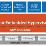
A growing technique for securing IoT and mobile platforms is partitioning tasks across processors. This way a secure wall can be built between critical functions and potentially malicious application code. Taking this a step further Mentor suggests using their Hypervisor to support virtual machines. Now a mix of operating systems can be used, and strong firewalls will exist between critical functions of the system and potentially vulnerable application code. This also works well for putting code that needs RTOS support on one machine and putting higher level OSs like Linux on another.
Baum outlined several scenarios where there is a mix of either homogeneous or heterogeneous cores. With current embedded CPUs it is feasible to run an RTOS in a virtual machine, or even in a bare metal environment (BME). Perhaps one processor is used solely to decrypt video and has specialized capabilities for this task. Another example is an elevator that does not need to use any resources until a BME core detects an occupant, at which time a Linux processor can be booted to interact with the user. In medical applications, tasks can be divided up for local and remote operations. Perhaps a medical device has a console at the bedside, but also occasionally needs to transmit data to a server for archival or subsequent analysis. These tasks can be coded for separate processors using the optimal OS and coding environment. Mentor’s Multicore Framework can facilitate this kind of development.
Data in the internet of things is vulnerable in several places. The most obvious is during transmission, but shared memory and IPC traffic are at risk, as well as data at rest. How many of us wipe our old phones before letting them out of our hands? Or do you prefer to smash them with a hammer? You have to think of the whole product lifecycle if you want to be comprehensive about security. Baum’s well taken point is that encryption does not equal security.
Mobile and embedded processors have evolved tremendously. The idea of multiple VMs running on multiple core CPUs in mobile devices would have seemed far-fetched a decade or two ago. ARM has even added type 2 virtualization to its A15 so that the Hypervisor itself can run as an application (guest) on a native OS. This means that even bare metal code or the guest operating systems are well contained within the underlying OS protections.
Mentor has a solid offering and lots of experience in the embedded space. It looks like Mentor has big plans for the internet of things and cloud computing. I’ll discuss the third presentation in another blog. The one teaser I can leave here is that it seems EDA companies are venturing far afield in looking for new business models. Look no further than Synsopsys’ acquisition of Coverity to get a sense of this.