webinar IPXACT banner

Customizable IP for HP and LP Audio Subsystems

Customizable IP for HP and LP Audio Subsystems
by Pawan Fangaria on 01-15-2015 at 4:00 am

Today, Smartphones and mobile devices have become center of innovation with multiple functions getting into them. Considering the audio or voice application, there can be multi-way conferencing, video chat, complete audio/video streaming, gaming, voice triggering and recognition,… you name an application, and it will be there on your Smartphone in most probability. While it has created so easy and flexible use of all these features in the hands of user, it has very significantly increased complexity in the hands of mobile SoC designers who need to deliver these features with high-performance, high-resolution, multi-channel audio stream processing, high quality speech recognition, always-on voice trigger, and all that at extremely low-power.

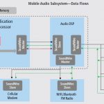
In audio/voice subsystems, DSP cores are used to handle data processing, compression, sample rate conversion, encoding/decoding, noise suppression etc. The audio DSP can be on an SoC along with the application processor or connected to the processor through a dedicated bus interface. The DSP core also connects to audio peripherals such as microphones and speakers, and cellular modem or WiFi/Bluetooth/FM radio combination through audio interfaces.

While this system is reasonably fine, the demand for high-performance audio data processing and voice over IP (VoIP) with improved noise suppression and noise-dependent volume control raises the DSP complexity and needs further improved architecture of the DSP and audio subsystem. Considering battery life criticality for mobile devices and always-on voice trigger, the system also needs to have very low-power profile. To satisfy these requirements, the DSP architecture must be very efficient with configurable memory and I/O partitions, advanced power management and scalable instruction set extensions. Along with DSP architecture, it is critical that audio data transport takes place in most efficient and optimized manner for low-power and high-performance. Interestingly, MIPI Alliance has also come up with new audio interface standards to optimize audio subsystem connectivity for the benefit of mobile industry. Let’s see in a greater detail the audio subsystem with improved architecture and new audio interface standards.

Here, the audio data transport is based on DSP-tunneled model instead of a common system memory to avoid multiple traversals of data on the bus hierarchy and the need to keep system memory and the bus hierarchy always powered. In the DSP-tunneled model, the audio data processing and transmit/receive through the audio interface are localized to the DSP processor with dedicated local memory and highly efficient FIFO-style interfaces; thus significantly reducing the power consumption.

The brand new audio interface standard used is Soundwire that is designed to support multiple devices including audio peripherals and DSP codec. It easily can be scaled up to support multiple data lanes to transport wide PCM audio samples between the application processor and the DSP codec. It can also be optimized to support the transport of narrow PDM samples to microphones and speakers on a single data lane. To minimize power, the standard defines a modified NRZI data encoding and double data rate for data transmission that minimizes active driving and switching of the bus wire load. The clock rate changing and clock stop protocols are well defined to minimize power consumption in always-on applications.

Cadenceis the leading provider of silicon-proven wide range of customizable IP for audio subsystem development. Cadence also leads the definition and development of the MIPI Soundwire standard.

Among Audio DSP IP, Tensilica Xtensa processor family offers highly customizable processor cores with high-efficiency instruction set architecture (ISA) extensions. A class of optimized HiFi processors targets various segments – HiFi Mini for voice trigger and recognition; HiFi EP for consumer electronics; HiFi 2 for mobile audio and voice; HiFi 3 for high-performance audio.

Among Audio Interface IP are I2S master/slave controller, S/PDIF controller, and MIPI Slimbus manager/device controller.

Cadence’s leading-edge audio DSP processor IP cores and audio interface IP cores are most suitable to build audio subsystems for high quality audio effects for multiple audio channels. Don’t forget to look at Cadence IP portfolio, if you are planning to build a low-power, high-performance, high quality, optimized audio/voice subsystem. Refer to the whitepaper for more details.

More Articles by PawanFangaria…..


Which Foundry will be First to FinFET?

Which Foundry will be First to FinFET?
by Daniel Nenni on 01-14-2015 at 8:00 pm

The final session of the SEMI Industry Strategy Symposium (The CxO Panel) was the most interesting for me because executives from three of the four most influential semiconductor companies were on the panel: Dr. Goeff Yeap of Qualcomm, Dr. Jack Sun from TSMC, and Mr. Mark Bohr of Intel. Who is fourth you ask? That would be Apple of course. In my opinion the most interesting question asked of the panel was: Which foundry will be first to FinFET?


The CxO panel closes the conference with a conversation between Dan Hutcheson and several esteemed executives at a CxO level. This year, we will be examining what it takes to practically transition a new technology to manufacturing and through its yield ramp. There’s no magic in it for these execs: they have to make finFETs yield today while rolling 10nm and 7nm processes down the gangway
from pathfinding into development. It is a task that has consumed many at prior nodes. They have closed their doors on Moore’s Law. Our panelists are the champions who won at these nodes and will keep moving down the scaling path. They will do this with a combination of their own internal excellence and an unparalleled ability to partner with others to align a global base of researchers and engineers — all towards hitting a specific ramp date that is exactly two years after the last one. They’re going to talk about how it’s done against a background in which every node gets bigger, faster, and riskier. They’ll provide their vision about the future, the challenges, and the opportunities.

Before I give you my ranking of which foundries will ship 16/14nm FinFETs first let me say a few words about Mark Bohr. I have always said the key to success in the semiconductor industry is showing up. Meeting customers and partners, writing papers or blogs, and attending conferences. Some call it collaborating but I call it showing up. Speaking at conferences is important too but if you only speak and do not actually attend that does not count. And don’t think we do not know who arrives right before their time slot and leaves right after because we most certainly do.

Mark Bohr not only spoke at ISS he showed up. I sat in the row next to him and chatted with him during breaks. He was not on his phone, he paid attention and took notes. He also graciously accepted a copy of “Fabless: The Transformation of the Semiconductor Industry” and I sincerely believe he will read it.

Which Foundry will be First to FinFET according to me:

[LIST=1]

  • Samsung 14nm LP Q1 2015
  • GlobalFoundries 14nm LP Q2 2015
  • TSMC 16nm FF+ Q2 2015
  • Intel 14nm 2H 2015
  • UMC 14nm 1H 2016

    Mark’s answer to the question by the way was “not Intel Foundry”. Another interesting comment from Mark was that Moore’s law will continue another 10 years but he says that every 10 years. Mark also explained to me the difference between the 14nm processes used for the Intel CPUs and SoCs. It really is the same process, same basic transistor structure, materials, design rules, and minimum interconnect pitches at the lower layers. The SoC version however has a wider range of devices (high-voltage and ultra-low leakage transistors) and a few more process steps. The bottom line is the processes are similar enough to run in the same “copy exact” fabs and that is quite an achievement, absolutely.


  • SEMI ISS: The Outlook

    SEMI ISS: The Outlook
    by Paul McLellan on 01-14-2015 at 12:11 pm

    I spent Monday at the SEMI ISS meeting in Half Moon Bay. There is a lot of stuff to choose from, the entire day was interesting throughout. The day started with a keynote from Scott McGregor, the CEO of Broadcom. I’ll cover that in a separate posting.


    Next up was Andrea Lati of VLSI Research on The Cycle: Is It Different This Time?He started with a review of 2014. Things that went right:

    • Apple’s A8 in 20nm at TSMC
    • Intel’s 14nm FinFET
    • EUV moving to production insertion at N10

    And what went wrong:

    • 450mm put on back-burner, won’t happen until 2023 or later (or never in my opinion)
    • 3D TSV still three years out
    • Electronics market continued to grapple with falling ASPs (commoditization of smartphones, tablets fizzled, electronic market overall growing slower than semiconductor)

    The answer to the question in the title of his talk was that magnitude of swings in the silicon cycle are much dampened when looking back as far as the 1980s. Equipment seems to be on a 2 year cycle for a couple of decades and based on history 2015 should be a good year. The big unknown: China goes nuclear to expand its semiconductor industry (for the 3rd time, maybe it will work this time).


    Next up, Mario Morales of IDC on What’s Next for the Semiconductor Market. By the end of 2015 he expects:

    • A base of 680M iOS and 1.7B Android devices
    • 3.3M apps available, 45-50 apps downloaded per year per device
    • But key market indicators are slowing
    • Tablet market his wall (iPad shipments actually declined) partially due to cannibalization by Phablets

    IoT will start in industrial where there are already massive amounts of data coming online. One machine at one plant might produce 1TB/day of data to be analyzed. IoT will then expand into the home. Challenges are low power, cost and security.


    Mike Corbett of Linx-consulting talked about materials. One interesting datapoint is that wafer cost is growing 41% node to node but the material node to node growth rate is 43%. As a result, materials are growing as a portion of wafer cost, especially sub 20nm due largely to all the additional material required for double patterning. DRAM is similar, with 9% node to node wafer cost growth but materials cost growing at 14%.


    Nariman Behravesh had his Top 10 Economics Predictions for 2015. So here they are:
    [LIST=1]

  • US growth will be solid in the 2.5-3% range
  • The European recovery will proceed at a sluggish pace but UK growth will be robust
  • Japan’s economy will regain weak growth momentum
  • China’s growth will decellerate more but remain stronger than most
  • A few emerging markets will struggle (Brazil, Russia) whilemany will see above average growth
  • Commdity prices will slide further (oil $60-70)
  • Inflation will remain a distant threat while deflationary worries persist
  • The US Fed, Bank of Canada, Bank of England will likely being raising rates while other central banks will be on hold or provide more stimulus
  • The US dollar will rise against most currencies while the Euro and Yen will fall
  • Perennial downside risks will be balanced by some upside risks (delveraging is largely over in US and UK, rising US oil production and the fall in prices is a $1.5T transfer, 2% of world GDP, from oil exporting to oil consuming countries)

    Finally, to wrap up the morning, Roger Baker of Stratfor gave a Geopolitical Forecast: Trends Shaping Semiconductor Manufacturing Countries. There was so much information it was like drinking from a fire-hose. But here are his key issues:

    • China is in a heightened sense of security and attempting an economic rebalancing towards consumption
    • Japan is attempting to brek from a 20-year malaise
    • Korea and Taiwan will be squeezed in the middle
    • ASEAN will exploit a slow but increased integration
    • US opportunities are expanding


    To pick one slide, China is attempting to push urbanization from 51% in 2011 to 70% by 2030. It plans to do in 17 years what took the US 50 years.


  • The Dynamics of the China Semiconductor Industry

    The Dynamics of the China Semiconductor Industry
    by Daniel Nenni on 01-14-2015 at 7:00 am

    Paul McClellan and I are at the SEMI Industry Strategy Symposium this week in Half Moon Bay. Honestly there is too much to blog about here so I will have to pick the topics most interesting to me. The full capacity audience is also impressive. SEMI provides a list of attendees on their website which reads like “Who’s Who” of the semiconductor industry, myself included. I may not be a “Who’s Who” yet but according to LinkedIn my profile is one of the most searched, so I have that going for me.

    One of the best presentations today was by Dr. Simon Yang of XMC in regards to the dynamics of the Chinese semiconductor industry. It was not canned, it was very real and full of experiences, observations, and opinions which is much more interesting to watch of course.

    XMC is China’s leading 300MM semiconductor manufacturing company. It was founded in 2006 in Wuhan, China and first began production in 2008. XMC provides its professional foundry service offerings to leading electronics companies worldwide. XMC focuses on developing specific customized solutions with its partners. Among its key area of expertise are memory and sensor manufacturing solutions. XMC is a recognized leader in NOR Flash memory production and BSI technology. XMC focuses on developing deep partnership and providing partners with tailored technology solutions to drive more innovation in the market.

    The Chinese government has been trying to bring semiconductor manufacturing to China for the past 25 years with very little success. The first China fab was a 6” established in 1990. An 8” fab was added in 1996. SMIC was established in 2000. 12” fabs were then added in 2006 and 2010. Unfortunately semiconductor demand in China has by far outweighed the ability to manufacture them. Currently China imports more than 50% of the world wide semiconductor supply while manufacturing less than 10%. Even worse, wafer manufacturing in China is less than 2.5% of the world wide production and is only at mature nodes (40nm and above).

    Simon quite honestly suggested that China manufacturing is much better at chasing slow versus fast moving technologies. Space travel and high speed transportation are two examples he gave. Another way to look at it is that with an advanced wafer manufacturing project you need to “do what you do not know how to do.” China is much more comfortable doing what they know how to do.

    Today semiconductor technology moves at lighting speed to satisfy the mobile SoC demand which drags along many more applications behind it. I do not see that changing anytime soon so this is a defining point for any country planning to make semiconductors part of their national agenda. For China it is not just satisfying internal semiconductor demand or national pride. In my opinion it is all about security. Electronics begin with semiconductors and so does the security of EVERY product that contains a semiconductor device, absolutely.

    Think about it, your smartphone knows your every move, your thoughts and secrets. Inside are billions of transistors that are “touched” by thousands of people. So how do you guarantee that all of those transistors are for good and not evil?


    2015 International CES: wearables and smart home

    2015 International CES: wearables and smart home
    by Bill Jewell on 01-13-2015 at 7:00 pm

    2015 International CES was held last week in Las Vegas. The Consumer Electronics Association (CEA) which puts on the show said over 170,000 people attended. The show featured more than 3,600 exhibitors covering over 2.2 million square feet of exhibit space.

    In advance of the show, CEA released highlights of its forecast for the 2015 U.S. consumer electronics market, measured as shipments to U.S. dealers. The overall market is expected to grow 3% from 2014. One of the fastest growing markets is wearables at 133%. Wearables includes smartwatches and health & fitness trackers. Smartphones are expected to grow 5% and account for 23% of the overall consumer electronics market. Tablets, which have been a hot growth item since Apple reinvigorated the market with the iPad in 2010, are projected to decline 1%. Overall televisions and displays are forecast to decline 2%, but 4K or Ultra High Definition (UHD) TV revenues should double from 2014.

    [TABLE] border=”1″
    |-
    | colspan=”4″ style=”width: 671px; text-align: center” | U.S. Consumer Electronics Market, $ Billion
    |-
    | colspan=”4″ style=”width: 671px; text-align: center” | Source: Consumer Electronics Association (CEA)
    |-
    | colspan=”4″ style=”width: 671px” |
    |-
    | style=”width: 167px; height: 21px” |
    | style=”width: 167px; height: 21px; text-align: center” | 2014
    | style=”width: 167px; height: 21px; text-align: center” | 2015
    | style=”width: 167px; height: 21px; text-align: center” | Change
    |-
    | style=”width: 167px; height: 21px” | Total
    | style=”width: 167px; height: 21px; text-align: center” | 217
    | style=”width: 167px; height: 21px; text-align: center” | 223
    | style=”width: 167px; height: 21px; text-align: center” | 3%
    |-
    | style=”width: 167px; height: 21px” | Wearables
    | style=”width: 167px; height: 21px; text-align: center” | 2.2
    | style=”width: 167px; height: 21px; text-align: center” | 5.1
    | style=”width: 167px; height: 21px; text-align: center” | 133%
    |-
    | style=”width: 167px; height: 21px” | Smartphones
    | style=”width: 167px; height: 21px; text-align: center” | 48.9
    | style=”width: 167px; height: 21px; text-align: center” | 51.3
    | style=”width: 167px; height: 21px; text-align: center” | 5%
    |-
    | style=”width: 167px; height: 21px” | Tablets
    | style=”width: 167px; height: 21px; text-align: center” | 25.2
    | style=”width: 167px; height: 21px; text-align: center” | 24.9
    | style=”width: 167px; height: 21px; text-align: center” | -1%
    |-
    | style=”width: 167px; height: 21px” | TVs & Displays
    | style=”width: 167px; height: 21px; text-align: center” | 18.7
    | style=”width: 167px; height: 21px; text-align: center” | 18.3
    | style=”width: 167px; height: 21px; text-align: center” | -2%
    |-
    | style=”width: 167px; height: 21px; text-align: center” | 4K UHDTV
    | style=”width: 167px; height: 21px; text-align: center” | 2.4
    | style=”width: 167px; height: 21px; text-align: center” | 5.0
    | style=”width: 167px; height: 21px; text-align: center” | 106%
    |-

    UHDTVs have become a mainstream product fairly quickly. In our 2013 International CES report, Semiconductor Intelligence stated: “The biggest visual impact was from 4K (or Ultra HD) TVs. With price tags of $20,000 and up and little content in 4K, 4K TVs will not have measurable impact on consumer electronics for a few years.” Now Bestbuy.com has major brand 55 inch UHDTVs for as low as $1000. CEA’s forecast of a $5 billion UHDTV market consists of 4 million units at an average dealer price of $1250.

    The hot product categories at 2015 International CES were digital health & fitness and connected home. The 2014 CES featured 366 exhibitors under the category of digital health and fitness. For 2015 the category was split into three (fitness & sports, health & biotech and wearables) and featured a total of 1,781 exhibitors, almost five times the number in 2014. The 2014 connected home category featured 982 exhibitors. In 2015 the number more than doubled to a total of 2,066 exhibitors in three new categories (smart home/appliances, safety & security, and energy management). The total of 3,847 exhibitors in these two categories is about equal to the total number of exhibitors at 2015 CES. Obviously many companies are classifying products in these categories as well as in the traditional CES categories. There is also likely overlap in the subcategories.

    Digital health & fitness and connected home are each part of the “internet of things” or IoT. IoT has been much hyped in the last few years as a major growth area for electronics and semiconductors. Many definitions exist, but the internet of things can be simply defined as any device which communicates over the internet and is not a computer, tablet or smartphone. These devices often communicate with the internet automatically without the need for human intervention.

    At 2015 CES, A&D Medical released the results of a survey of 2,024 U.S. adults conducted by Harris Poll. The survey showed 56% want to monitor their health with connected devices. The most desired vital signs the participants wanted monitored were blood pressure, weight, chronic conditions such as diabetes and hypertension, sleep, physical activity and diet. Only 5% wanted to monitor their sexual activity. However that low number did not stop OhMiBod from introducing a product in the category of wearable sex technology. We won’t go into detail here, but the specifics are in OhMiBod’s press release.

    The 2015 CES Innovation Awards featured several products under the categories of wearables; fitness, sports & biotech; and smart home.

    The Polar V800 (below) is a multisport GPS watch for activity tracking and fitness training with a list price of $520. It not only looks complex, the manual is 102 pages.

    The Withings Activité in contrast is a simple and elegant looking analog watch which doubles as an activity tracker and retails for $450.

    The Cloud Based Advanced Smart Robo VacMop from Moneual learns from prior cleaning history data saved on the Cloud. This device could be also be classified under “things we didn’t know anyone needed” and “fun things to scare your cat.”

    Also from Moneual is the Smart Beauty Mirror, an integrated grooming gadget with a mirror that “provides personalized fashion and beauty care information through face analysis, skin monitoring, trending fashions, web contents and more.” Now every woman can have the magic mirror the evil queen had in Sleeping Beauty.

    Netatmo’s WELCOME is a smart home camera with facial recognition. “It learns to recognize your household members and updates you on who is home when you are not, with concise notifications on your smartphone or your smartwatch.” Good way to keep your home safe and spy on who is with your kids when you are not home.

    It is difficult to predict which of these products will be successful. However the “internet of things” is more than just hype – it is a fast growing area of consumer electronics.


    HiFi Sounds Better than Ever

    HiFi Sounds Better than Ever
    by Eric Esteve on 01-13-2015 at 12:00 pm

    If you think that the sound atmosphere created by Dolby or Surround–sound audio is the best you can achieve today by using complexes algorithms on DSP, like I thought before knowing about “Object-Based Audio”, you must read these lines! In fact Surround-sound Audio is limited by the number of speakers installed in a room, or a car, and the number of available channels. With Object-Based Audio, the sounds can be moved around the listening space regardless of the number of speakers. Just take a look at the picture, the numerous grey dots represent the perceived sound sources. Such a technique is already magic if the listening space is a room. Imagine your perception of the sounds when Object-Based Audio will be installed in an automobile, a listening space where adding speakers is quickly limited by some obvious factors…

    Object-Based Audio sounds magic, but I will unveil the trick. The trick’s name is HiFi 4, the latest DSP core from Tensilica/Cadence. As you need high performance for such emerging audio, this HiFi 4 DSP support four 32×32-bit MAC per cycle with 72-bit accumulators then a single HiFi 4 DSP IP core can replace multiple DSPs, for example in high-end DTV and STB applications. With Object-Based Audio, control and signal processing loads have significantly increased, and HiFi 4 has been specifically tailored to make sure that a single DSP IP will support these extra loads, including an optional vector floating point unit.

    It was not by chance if Cadence has grown DSP IP revenue from $6M in 2012 to more than $48M in 2013, allowing the IP vendor to be ranked #1 in this segment by Garner. Cadence claims counting more than 65 licensees to date, for the HiFi Audio DSP IP only, not integrating Tensilica Dataplane product. You can find HiFi Audio DSP IP integrated into Mobile Phones, Consumer Electronics, PC and Tablets, STB, Blu-ray Disc, AVRs and Automotive Entertainment. If you take a look at the various logos printed below, you can see that HiFi DSP is popular with Tier 1 semiconductor companies like Intel, Samsung, ST, NXP, Renesas, Fujitsu or Dialog and also with many system companies like Huawei, Wolfson or LG, to name a few.

    The first and large application field for DSP has been the baseband for mobile phone since 2000, allowing the chip makers to familiarize with the DSP IP core concept and integration (before 2000, the semiconductor companies targeting wireless market tend to use their own DSP, think about Motorola or Texas Instruments). But a DSP can be used to support much more than convolutional coding or Viterbi algorithms! Audio has been a long time (almost) captive market for Motorola, thanks to their 24-bit DSP standard products. This explains why the first HiFi and HiFi 2 introduced by Tensilica at the beginning of the 2000’s were integrating 24-bit Dual MAC: potential customers using Motorola DSP would accept to move to a DSP IP solution, but only if they could stay with the familiar 24-bit DSP architecture, and reuse the S/W base.

    At the end of the 2000’s, Tensilica has introduced the first 32-bit architecture (still with a 24-bit dual MAC), allowing a better pre and post processing, but the next product was based on a dual 32-bit architecture. Audio applications were developing fast and the most the performance improved, the more attractive could be the audio solutions. You can easily draw a parallel with Video, HiFi 3 was launched at the same time than 2K video, and we could say that HiFi 4 represents a performance jump equivalent to the move from 2K Video to 4K. The difference is that the HiFi 4 DSP can support a revolutionary audio concept, Object-Based Audio, and the DSP ecosystem includes more than 140 software packages compatible across all the Hi Fi cores.

    If we want to synthesize Cadence/Tensilica HiFi DSP IP family offer, we could say that the HiFi 3 target markets are Mobile, Home Entertainment and Automotive, when HiFi 4 is more dedicated to Home Entertainment and Automotive high end applications, like Object-Based Audio. In fact for Mobile applications the balance between power and performance would push to use HiFi 3. Just like implementing 4K video resolution on a smartphone does not really make sense (except maybe as a pure marketing argument!). Interesting to notice, the HiFi Mini is specially tailored to support Voice Trigger & Recognition, sensor fusion, Always-on functions… sounds like this is the right DSP IP product to support IoT, exhibiting the lowest power of the WiFi family.

    By Eric Esteve from IPNEST


    A Group of Happy Employees that Excels in Everything They Do!

    A Group of Happy Employees that Excels in Everything They Do!
    by Pawan Fangaria on 01-13-2015 at 9:00 am

    I visited AtrentaNoida in August 2013 during the inauguration of its newly expanded facility. At that time, I had written about the beautiful environment Atrenta has, with its presence at many sites across the world in my blog – “Innovation + Thoughtful Management = Productive Expansion”. Innovation cannot happen without happy employees gelling with each other, bringing out the best in active teamwork with the support of management, to promote learning from failures rather than scrapping the project altogether. Innovation doesn’t come without risks and failures, management understands that. At the same time, the work place must be fun with a healthy work-life balance, along with an open, cooperative and trustful culture. I had many chances to visit Atrenta Noida during these years, and I could personally see that kind of environment there.

    There is no wonder, I am seeing this video today, made by the enthusiastic people at Atrenta talking about their happy times in the company, how they spend the days and weeks, what they do, how they feel proud ofworking with top chip design companies, and their EDA tools being used in designing top electronic products. They also discuss how they publish technical papers and patents and so on.

    Not being sure where to start, as a natural instinct, I choose to start with fun moments; play, games, fitness enthusiasts. It reminds me of my basic graduation professor at my college; he used to say that those who excel in the field will excel in class as well. Atrenta has a world class facility connecting Noida with rest of Atrenta’s sites in the world. It has all kinds of infrastructure including data centres for 24/7 operation.

    Here people are gearing up to look at the bigger picture presented by their leaders. On the left side, Sanjiv Mathuris presenting some new architecture, algorithms or methods for one of their products; on the right side, Siddharth Guhais preparing to present some information on SpyGlass Power. I can just guess about the products on which they would be presenting since I have talked to them and blogged about their products in the past!

    Then there is a brainstorming session going on one side of the room while there is a serious discussion on the other. At Atrenta, it’s a good practice to have small team sizes for particular projects / sub-projects that provide optimum productivity. During work time, people have best presence of their minds.

    There is also a wall of patents. This reminds me about my discussion with Ajoy K. Bose, President and CEO of Atrenta; he said most of their patented ideas are realised in their products. What could be more productive then this? This is profitable to business, brings cheers among employees, encourages team morale, and provides a confident outlook for the organization. The team is enthused to publish and present technical papers at various conferences.

    Here there is a relaxing moment, out of serious work, for people to chat and lighten up. Then there is a person seriously glued to his laptop and code to resolve a potential issue, urgently for a customer. At Atrenta, 75% of the 350+ work force is in R&D and still they are able to satisfy 250+ customers across the world. That is because of very flexible work environment that boosts productivity as well as work satisfaction among employees.

    The Atrenta culture promotes social activities with a lot of enthusiasm; year over year, people celebrate important occasions. Above, people are celebrating last Thanks-Giving day where senior managers are serving food to employees. People pay thanks to their peers, managers, staff, and colleagues and even in their neighbourhood. As part of their CSR (Corporate Social Responsibility) initiative, they regularly organize blood donation camps and various other activities.

    Here is the whole Atrenta Noida Team standing together under one umbrella. I’m sure many people are standing on the second and third floors of this Speciality Tower joining in the team spirit.

    Atrenta is a true global organization with equal participation from all of its sites (R&D, Field and Sales) in USA, Europe, India, Sri Lanka, Taiwan, China, Korea and Japan. There is great level of collaboration between the sites to access best talent and support customers across the world in most cost effective manner.

    More Articles by Pawan Fangaria…..


    Twelve Years of Sonics at Toshiba

    Twelve Years of Sonics at Toshiba
    by Paul McLellan on 01-13-2015 at 7:00 am

    Sonics announced today that Toshiba has completed the SoC design using Sonics’ on-chip network IP for its new TZ2100 group of application processors. The TZ2100 group of applications processors are the newest addition to Toshiba’s ApP Lite (Application Processor Lite) TZ2000 series. With this group of ApP Lite devices, sound and image communications can be securely processed at high speeds, making them well-suited for applications such as smart appliances, industrial CPUs, panel-control systems, and machine-to-machine [M2M] communication modules. The IoT will see more and more devices connected to the Internet and to each other. Increasingly, functions to effectively process and safely transfer a wide variety of data, from simple text to data-heavy audio and visual sources, are required for IoT. ApP Lite microprocessors are ideal for such processing.

    What is perhaps even more significant is that Toshiba have been using Sonics NoC technology for 12 years and have completed over 30 designs. Cumulatively they have shipped over 200 million SoCs in which Sonics’ NoCs serve as the communication fabric. These cover a wide range of different target markets: gaming, digital TV, mobile, and automotive applications, and now the TZ2000 series, application processors. As you would expect, over those dozen years the designs have got increasingly complex in terms of both the number of IP blocks integrated and the performance, both increasing clock speed and using increasingly advanced process nodes.

    Katsuya Konisha, who is GM of the Logic LSI Design Department emphasizes that Toshiba will be continuing to use Sonics NoCs going forward:Sonics’ on-chip network products play a critical role in the integration of our complex SoC designs. They help us achieve the time-to-market and performance requirements for these projects. We are very pleased to reach this important milestone in our relationship and plan to continue using Sonics’ IP in our ASSPs and ASICs.

    Sonics also announced that that Nexell has licensed SonicsGN and adopted the SonicsStudio Director development environment for creation of a customer-specific application processor design targeted to the digital consumer and communication systems market segments. Nexell, founded in 2009, is a Korean-based developer of SoCs, semiconductor IP, and application processors. The company plans to target its new application processor design, which includes the SonicsGN NoC, for manufacturing in Samsung’s 28nm low-power Gate First High-k Metal Gate (HKMG) foundry process technology. Nexell will use SonicsStudio Director as its SoC integration environment to drive design and verification within the Samsung EDA tool and manufacturing flows.


    UPDATE: the webinar has been moved to Wednesday February 4th.

    Also, I will be moderating a new webinar Using SonicsGN to Address Low Power Requirements from IoT to Servers. The webinar will be at 10am Pacific on Wednesday February 4th. The webinar itself will be presented by Drew Wingard, the CTO of Sonics.

    For more information on the webinar, including registration, go here. On that page you can also view the last Sonics webinar that I moderated, NoC 101. This is an introduction to network-on-chip technology for designers who are unfamiliar with the concept.


    Semiconductor Design: Chips to Systems!

    Semiconductor Design: Chips to Systems!
    by Daniel Nenni on 01-12-2015 at 8:00 pm

    This is the 20[SUP]th[/SUP] year of DesignCon and I’m really looking forward to it. While I haven’t attended all 20 I certainly have attended the majority of them. Now it is like a college reunion for me seeing all sorts of friends and former coworkers. One of them is even a keynote but more on that later. This year there are 14 conference tracks covering semiconductor design through to the system level with more than 100 sessions, panels, and tutorials. Take a look HERE for the conference overview.

    My good friends at Mentor Graphics are a platinum sponsor this year with Technical Workshops on:

    • DDR Interface and SerDes Channel Design for High Performance FPGA – based PCBs
    • Electromagnetic Simulation for Electronic Systems
    • Designing Manufacturable Stackups – A Comprehensive Approach to Stackup and SI Modeling
    • A Holistic Approach to IC, Package and Board co-optimization
    • DDR4 Board Design and Signal Integrity Verification Challenges
    • Accurate statistical analysis of SERDES links considering correlated input patterns, data-dependent edge transitions, and transmit jitter

    Mentor Graphics® is the worldwide market leader in PCB systems design and analysis technologies. Mentor Graphics will be showcasing its advanced HyperLynx and Nimbic technologies for electrical sign-off, including a complete analysis environment for DDRx designs, multi-gbps channel analysis, full-wave 3D electromagnetic modeling, and power distribution design. Visit booth #935 to learn more about Mentor’s technologies and best practices for virtual prototyping or by attending Mentor Graphics technical presentations.

    You can also visit their booth and spend some quality time with experts in the field of signal and power integrity analysis, IC/package/board co-optimization, and automatic stack-up design.

    Here are the conference tracks that cover all aspects of chip, board, and system design:

    [LIST=1]

  • Optimize Chip-Level Designs for Signal and Power Integrity
  • Overcome Analog and Mixed-Signal Modeling and Simulation Challenges
  • Wireless and Photonic Integration
  • System Co-Design: Chip/Package/Board: Modeling and Simulation
  • Characterize PCB Materials and Processing Characterization
  • Apply PCB Design Tools
  • Design Parallel and Memory Interfaces
  • Optimize High-Speed Serial Design
  • Detect and Mitigate Jitter, Crosstalk, and Noise
  • Leverage High-Speed Signal Processing for Equalization and Coding
  • Ensure Power Integrity in Power Distribution Networks
  • Achieve Electromagnetic Compatibility and Mitigate Interference
  • Apply Test and Measurement Methodology
  • Ensure Signal Integrity with RF/Microwave/EM Analysis Techniques

    This year there are insightful keynotes on Tuesday, Wednesday, and Thursday by industry luminaries:

    [LIST=1]

  • Thomas H. Lee Ph.D, Professor of Electrical Engineering, Stanford University
  • Karen Bartleson, Senior Director of Corporate Programs and Initiatives, Synopsys
  • Alex Lidow Ph.D, CEO, Co-Founder, Efficient Power Conversion Corporation

    Karen is the friend I mentioned. She is very active with IEEE and is currently a candidate for IEEE president! Congratulations Karen! I will be at DesignCon all three days and it would be a pleasure to meet you!

    Taking place annually in Silicon Valley, DesignCon was created by engineers for engineers and remains the largest gathering of chip, board and systems designers in the country. Combining technical paper sessions, tutorials, industry panels, product demos and exhibits, DesignCon brings engineers the latest theories, methodologies, techniques, applications and demonstrations on PCB design tools, power and signal integrity, jitter and crosstalk, high-speed serial design, test and measurement tools, parallel and memory interface design, ICs, semiconductor components and more.


  • Je Suis Charlie

    Je Suis Charlie
    by Eric Esteve on 01-11-2015 at 4:48 am

    Last Monday was the first working day of 2015, dedicated to installing a new PC. Tuesday was also dedicated to an admin work, asking for a new passport, so Wednesday was supposed to be the first real working day for me. In fact, because the Radio is on when I am working, I heard about this crazy offense against the complete editorial board in working session at “Charlie Hebdo”, a French caricature fanzine, a few minutes after it happened. In less than 5 minutes, the entire cartoonist band, Cabu, Wolinski, Charb. Tinious and Honore, plus some of their occasional writers and friends and the policeman supposed to protect the fanzine’s director (and two other persons in the building) have been killed by two terrorists using Kalachnikov… It was Kalachnikov against pen, fundamentalism against humor.

    Before going further and propose my humble contribution against middle age obscurantism, let me add that these two terrorists have eventually been neutralized, being killed on Friday, but that a third one had time to attack a casher grocery that same day, killing four hostages before being killed as well. These grocery customers have clearly been killed because they were Jewish, such an action recall us what’s happened in Berlin in the 1930’s. These “terrorist” are just barbarians.

    To come back to the cartoonists’ massacre, these artists have been killed because they have used their pen to caricature Mahomet (in fact to critic the positioning of a very small part of Muslims, using the religion as a weapon, and dropping bombs instead of trying to convince). You may think that these journalists have been provocative… and that’s true! But the key point is that they are provocative with every religion, Catholics (see above), Jewish, Muslims and so on, they are also provocative with (all) the political forces, and definitely with any kind of hypocrisy, including the politically correct. To be fair, I must say that before this massacre, many French people did not like this type of humor, that we call “Humour Gaulois”. This “Humour Gaulois” is not characterized by subtlety or delicacy… but is it a reason for killing? Beside this clumsy humor, you can quickly find a way of thinking linked to Enlightenment, Voltaire et al., these same persons who have been the source of the French revolution in 1789 or the USA Independence in 1776. Voltaire was saying: “Even if I don’t like your ideas, I will fight as much as I can to allow you to express it”.

    As far as I am concerned, on top of trying to kill freedom of expression (but they will not succeed!), these stupid terrorists have killed part of my youngness. If you take a look at the above picture, it was published in the early 1970’s by Cabu (RiP on Wednesday) in a fanzine dedicated to teenagers like me. I perceived these images as my first teenager emotion, a teenager able to select by him what he wanted to enjoy with (and not what the religion or the politics expect him to enjoy). Since Wednesday I am sad, for me and for my culture, and I am angry too, and I am not alone to be angry as probably more than one MILLION peoples will silently walk today in Paris. Including politics from Germany, England, Israel, Palestine, including people who did not really liked Charlie Hebdo, including Jewish, Catholics, Protestants or even Muslims. All of us will claim: “Je Suis Charlie”!

    Note to a potential moderator: this is not a political or religious blog, just a request to keep freedom of expression as strong as possible. Moderating this blog, even by auto-censure, would be a way to reduce this freedom of expression.

    Eric Esteve