By this time, anyone with a pulse in the tech industry knows that Apple has dual sourced the A9 processor for the Iphone 6S, from both Samsung and TSMC. There are even apps to tell whether your 6S has a Samsung or TSMC part in it. People have run performance comparisons and concluded that the processing performance is the same, which is entirely expected as we are sure both parts have the exact same logic design and are clocked at the same speed. Ones and zeros are ones and zeros on anyone’s chips….all things are equal in the digital world….
Well…people have started to check in on the analog world of power consumption (where there can be a difference) comparing Samsung Iphones to TSMC Iphones, and low and behold the Samsung and TSMC made chips may not be quite so identical. Initial, amateur reports indicate a significant difference with Samsung parts consuming more power….far more..
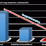
Here is an example of one such test result:
Samsung A9 versus TSMC A9 power consumption tests
We would remind readers That TSMC has made a very big deal about their power consumption/leakage advantage over other competitive manufacturing processes. TSMC has claimed up to a 20% power advantage in their 16nm process which may jive with these unconfirmed comparison results.
Any measurabledifference could be a problem for Apple..
The initial results look like a significant power consumption difference between the Samsung A9 and the TSMC A9, potentially measured in hours rather than minutes. Even if final analysis shows a 10% differential or less it could still pose a problem as Apple could start to see 6S owners returning their Samsung 6S for a “better” TSMC 6S. The bad press could really hurt Apple and its flawless image very badly.
We think the difference better be less than 5% or problems will start. A 10% differential in power consumption would be bad, a 20% difference could be horrible and so on…costs and losses could mount up for Apple for returns, repairs etc;…. Even if these initial reports prove to be untrue and there is no significant power difference just the rumor mill buzz of two types of 6Ss can cause issues.
Cottage industry for phone testers…
There are already different apps that can tell which processor you have in your Iphone. One even reports the results back to a website that keeps score of TSMC versus Samsung parts. We can imagine that cell phone repair shops will charge customers $20 to see if they should return their beloved Iphone because it has a potentially flawed Samsung A9…..
Faster than you can say class action lawsuit
Lets start the stopwatch ticking on Oct 7th at noon and see how long before the first law firm brings a class action suit against Apple and their defective Iphone 6S. Will Apple have a recall? How will they handle the PR? It could be a circus of TV people interviewing people at Apple stores as they return their phones….just in time for the holiday season
Conspiracy theories?
We can only imagine the first conspiracy theory that Samsung did it on purpose to sabotage Apple’s phone business in favor of their own…..
Blowback on Apple due to supplier gamesmanship…
Apple is well known to press suppliers to the breaking point and beyond. Apple went to a new extreme and got very cute by dual sourcing the most critical component in the phone this way playing Samsung and TSMC off against one another. Could this now have blown up in their face? Who tested and vetted both parts at Apple? Where’s the quality control?
We would question why Apple would even take the risk of using two different parts in the same phone….its just begging for comparison & trouble. Just use one part in the 6S and the other part in the 6S plus so you can’t compare them. Maybe Apple was forced into this position due to availability issues.
In too much of a rush?
We had pointed out almost a year ago that we were surprised that Samsung would be able to get the 14nm part out in time for the 6S launch. Early yields were low and Samsung would have to ramp faster then ever before to make it in time. Maybe it was just too fast a ramp and the part and the process was never fully perfected leading to the power issues.?..
Intel’s schadenfreude…
If this turns out to be true and a significant issue we will likely be able to hear the laughter in the halls of Intel all the way in New York (Intel had their own mathematically challenged processor many years ago). There has obviously been concern over Samsung and TSMC catching up to Intel….well maybe this could potentially prove at least Sasmung moved too fast and took too many risks versus Intels more cautious slowing of their tick tock cadence.
Speaking of Intel, we are pleased with the performance of the stock, nicely and steadily up well over 10% since we turned positive on it a few weeks ago…looking better every day
Leaky faucets and transistors…
Transistors are like faucets turning on and off the flow of electrons or water, however transistors never fully turn off and tend to “leak” a little. This “leakage” is the primary culprit of power consumption in semiconductor devices.
Leakage in transistors is due to a multitude of factors, many of which are interrelated. Transistor design is a big one, especially as the industry has recently switched from “planar” to “FinFET” transistors (which Intel pioneered). Materials and the processing of those materials by semiconductor equipment tools is very critical. Many different tools and materials impact leakage current.
Though the logic design of Samsung and TSMC’s A9 is the same, the manufacturing process “flow” is quite different, using different sets of tools and materials and different steps in different sequences. TSMC has strongly made the claim that their 16nm process is superior to competitive offerings in terms of leakage/power consumption.
Samsung is 14nm while TSMC is 16nm…
Smaller is usually better in the semiconductor industry but everyone’s measure is not quite the same. Samsungs A9 uses a “14nm” process which results in a smaller die size (chip size), while TSMC uses a 16nm process that results in a larger chip which is usually associated with higher power consumption, but not this time around, making the potential difference even more intriguing.
If Samsungs 14nm process proves to be inferior to TSMC’s 16nm process that will be a boon and huge win for TSMC and a huge loss for Samsung on the foundry side (aside from the obvious Apple problems). It could be a huge torpedo in the side of Samsungs Semiconductor business which has been their primary driver of profitability.
What about the equipment companies?
We can already hear the equipment companies taking credit for their equipment making the difference at TSMC and Samsung. If its does turn out to be equipment specific it would obviously have huge impact (Cue Art Z and UTEK) . We would imagine this has to be positive for process control companies like KLAC and smaller cousins Hermes, RTEC, NANO and NOVA etc;. Everyone will clamor to find out the root cause.
This could turn out to be a circus…
This has all the makings of a potential circus in the industry and in the stocks. Certainly negative to very negative implications for Apple if true. Negative for Samsung and positive for TSMC. Likely positive for some equipment companies but not all. Positive for Intel as it shows their process still reigns supreme.
There are many , many moving parts and right now we still don’t even have solid proof that an issue even exists or enough information to analyze but we do understand the potential implications and want guard our portfolio against them.
We will be waiting for more information and definitive tests…..
Meanwhile…I am going to test our families new Iphone 6S and get in line to return it at the Apple store if it has a Samsung A9 before the rush happens……
*Disclaimer: So far we have not seen a credible, reliable, scientific source of comparative power consumption testing – sources on the internet appear to show similar results but are unsubstantiated and therefore questionable so far…..
Robert Maire
Semiconductor Advisors LLC