In the first part of this article I wrote about four types of costs which must be considered when an IP goes through design differentiation, customization, characterization, and selection and evaluation for acquisition. In this part of the article, I will discuss about the other five types of costs which must be considered to enhance the value of IP and keep the IP-based SoC business model growing. In general these costs are known by their simple terminology; however they need to be better understood in the modern context of IP so that the right level of investment in the IP can be justified from both sides – the IP provider and the SoC integrator. Let’s analyze these in their right perspective here.
Cost of Qualification – The quality of IP, specifically design IP is a big question mark today. As you obtain the third-party IP blocks from different regions (which may have different quality culture) of the world, it’s imperative that they must be qualified in the premises of the SoC integrator before they can enter into the works. A preliminary assessment and evaluation of an IP must have been done as part of acquisition, but its actual qualification from quality and security perspective according to its intended use in the actual SoC environment must be done in-house by the SoC vendor. For example, an IP for automotive applications must be tested in the SoC environment under the intended temperature ranges and possible electromigration effects. This is essential to ensure the IP is bug-free to avoid resolving the IP bugs at the system-level which can be very unworthy and extremely costly. It’s not a complete verification of the IP or system; I will talk about verification in detail in a subsequent section. It’s a quick qualification of the IP in focus. Fractal Technologieshas a tool called Crossfire which has an option to quickly qualify your IP with all formats and the SoC environment in which the IP is intended to be used. Similarly there is IP Kit from Atrenta (now Synopsys) available at TSMCfor partners to qualify their soft IP against Atrenta’s SpyGlass provided checks. There may be other commercial or internal tools as well to assist in this acute need of qualifying the IP before its use.
Cost of Integration – Although the cost of integration of an IP into an SoC falls into the purview of the SoC vendor, the onus of integration may come on the IP provider who needs to make sure the IP or subsystem along with the software bring-up works properly in the SoC environment. The matter of the fact is that the SoC integrator does not understand all of the IP that are going to be integrated into the SoC; so the SoC vendor has to hire domain experts in different areas. The IP provider in most cases has to work at the subsystem level when integrating an IP into an SoC.
For an IP provider it’s like envisioning the system requirements and making provisions for those while working at the IP level. For example, in case of an interface IP the whole channel has to be modeled as per the system requirements; for a physical IP, the PPA has to be modeled with right level of trade-off according to the system requirements. The PHY has to be programmed to make a trade-off between PPA. In modern age, the range of PPA can be very wide in which case the IP has to be segmented into high-range for performance critical applications, mid-range to save power, and low-range to save cost. Again, for an IP with FinFET and smaller geometries, you may need to increase the area to spread the heat. Also the FinFET process varies between foundries, so if you are sourcing an IP from two different foundries, then you will also have to spend in unifying those characteristics to keep the final SoCs uniform. As an example Applesourced A9 SoCs for its iPhones 6s and 6s Plus from TSMC 16nm as well as Samsung 14nm foundries. So, at the system level their characteristics have to be matched to keep the power and performance uniform for all phones.
Another level of complexity comes when you integrate analog with digital on the chip. The analog portion needs confirmation from the foundry, so it’s advisable to keep the analog content as less as possible. However moving things from analog to digital can be another complexity and will surely incur cost.
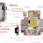
Considering an IP from system perspective, it’s important that the package aspects are taken into account. This includes effects such as noise, signal integrity, ESD, and so on.
More and more of system companies prefer team integration with the IP vendors where the IP team can work with the system team and contribute in SoC roadmap development for future innovative technologies. This is a smart move for giving a lead time to future technologies, provided confidentiality is maintained. These days we are also seeing full merger of IP companies into SoC companies. A flip side to these mergers is that a sustained continuation of such mergers may defeat the purpose of IP-based business model in the longer run.
While integrating an IP into an SoC and optimizing it within the cost parameters for a particular target segment, the integration has to go through several trials to obtain the best optimized architecture. To save the cost of these trials, the IP and SoC industry is gearing towards automating this effort.
ARMhas already developed tools for such automation. In the picture above there is ARM[SUP]®[/SUP] Socrates[SUP]TM[/SUP]design environment along with CoreLink[SUP]TM[/SUP] Creatorfor interconnect optimization and CoreSight[SUP]TM[/SUP] Creatorfor debugging. Read the article, “New Tool Suite to Accelerate SoC Integration” for more details on the “ARM IP Tooling Suite”.
Cost of Verification – This is the most significant cost in an SoC, almost 2/3[SUP]rd[/SUP] of the total cost of the SoC. There are multiple verification engines for simulation, emulation, formal verification, virtual prototyping, FPGA prototyping, and post-silicon verification at different stages of an SoC design. The key idea is verification closure through complete coverage of the overall SoC. It’s in general very difficult and hard problem to get complete coverage of an SoC. These days the SoC vendors bring up the whole system and run applications on full chip through emulation, or validate the SoC through FPGA prototyping which has its own limitations. There is no way to guarantee complete verification other than the verification coverage metrics, so coverage driven verification gained importance where coverage obtained through different verification methods gets added up.
With the expansion of SoC’s size and complexity including hardware, software, and firmware, the verification space of SoC also has expanded enormously. In such as scenario, imagine a configurable IP getting added up. How do you ensure all of its configurations are validated? It expands the verification space further, multiplied by the number of configurations. This keeps the cost of verification increasing.
In the IP-based business model, along with the design IP, the idea of verification IP (VIP) also came with the sole intention of verification automation and reuse of test plan, test bench, and test suite across multiple designs to boost verification productivity. Similarly, standard verification methodologies came into practice for verification automation and testbench reuse, UVM (Unified Verification Methodology) being the most popular. However, UVM is good for IP and at most subsystem level. The system level test is the bottleneck and that is where the verification space blows up. At the system level, as we have seen, there are multiple verification engines in work and there are multiple IP and subsystems. There is no automated methodology and reuse of tests and testbench across these multiple design levels and engines. This increases the cost of verification exponentially.
To automate verification and reuse at the system level, key initiatives are going on to establish software driven methodology based on use-cases and test scenarios. Accellerahas initiated a Portable Stimulus Working Group (PSWG) to establish a common standard of test and stimulus which can be used by a variety of users across different levels of design hierarchy (IP, subsystem, and system) under different execution platforms (simulation, emulation, FPGA prototyping, post-silicon, or any other) using different verification tools. Cadence, Mentor, and Brekerhave developed tools for system level verification; and they along with other PSWG contributors are working on establishing the common test standard and making their tools compliant with this standard. This can definitely start a new chapter in verification from system-level and reduce the burden of cost of verification by a large extent through test automation and reuse across multiple design hierarchies as well as verification engines. However, this methodology is yet to be established and needs semiconductor industry level investment, effort, and time. Read the article “Moving up Verification to Scenario Driven Methodology” for more details on this initiative.
Cost of Learning – As the complexity of SoCs keeps growing the verification space is always open for new learning. In the last section, we talked about the use-case based verification methodology which is being explored for verification at the system-level. Even after this methodology is established, there will be a cost involved in training the verification engineers on this new methodology.
In verification space newer formats, protocols, and standards keep emerging, especially in IoT, mobile, and automotive segments. This needs budget, time and effort set aside for design and verification engineers to learn. Moreover, the verification engineers need to have complete knowledge about the system and the environment or market segment in which the system is going to operate.
Apart from the system and design, the learning has to happen at the process and foundry level as well. The advanced process nodes such as FinFET nodes are distinct with foundries and hence the learning effort gets multiplied. The design, verification, and process engineers need to work closely to understand the new process and its associated rules. The process engineers may need to work in the actual foundry environment to learn about the advanced technology aspects and impart that knowledge to the design and verification engineers for them to incorporate the same in the design and its verification.
Cost of Redundancy – A peculiar scenario arises when you configure an IP to serve multiple requirements for different market segments. Not all the segments are served at the same time, so there are unused portions in the design and those can vary in different situations. This brings redundancy along with configurability. The redundant circuit may also consume power unnecessarily if not architected well enough to remain shut when not in use. Such wastage of power may not be completely eliminated through multi-mode operation of the SoC. Another case of redundancy comes when an IP characterized for a particular technology node is no longer reusable for another technology node through the use of automated technology migration tools; the IP needs a fresh architecture and rework. In such cases, a proper ROI analysis must be done for the IP to remain profitable in single use.
Summary – There are methodologies being explored to reduce different types of costs through automation. However, it depends on the specific methodology and the type of cost that can be reduced. Moreover, the automation methodologies such as system-level synthesis and verification need to be established before they can be explored for wider use. Intermediaries such as eSilicon have come up that provide IP services for SoC vendors to do a pre-evaluation of IP integration into their SoCs before buying it. The eSilicon business model is very flexible where they can be paid for an IP either after pre-silicon evaluation or after production. The semiconductor ecosystem is trying to establish a series of drivers that can keep the IP costs in control and the IP-based SoC development model afloat.
First part of this article is HERE.
Pawan Kumar Fangaria
Founder & President at www.fangarias.com