Looking back, 2015 was a significant year for mergers and acquisitions in the EDA industry. The Semiwiki team maintains a chronology of major transactions here.
As I was reviewing this compendium, one of the entries that stands out is the acquisition of Apache Design Solutions by Ansys, Inc. a couple of years ago.
At that time, there was some uncertainty expressed as to the synergy between the two firms, one being rather system-centric and the other focused on the analysis challenges of deep submicron chip designs. Many assumed that Apache would be an acquisition target of the purple, red, or green EDA company, rather than Ansys.
Ansys is a premier supplier of package, board, and system-level tools for electromagnetic and mechanical analysis. The HFSS finite-element analysis and SiWave simulation tools are the gold standards for extraction and simulation of complex time- and frequency-domain characteristics of package/board traces, for signal integrity and power integrity (SI/PI) loss assessment. As SerDes channel data rates continue to be pushed aggressively by system designers, the required accuracy of the SI models necessitates the precise models available from HFSS. The Ansys Multiphysics tool suite provides several (coupled) analysis capabilities:
- mechanical analysis of materials stress and deformation to evaluate attach and assembly reliability
- electromagnetic propagation analysis for EMI compliance, and
- thermal modeling to ensure reliable system cooling
As a startup in the early 2000’s, Apache developed the leading RedHawk toolset for chip-level IR voltage drop and electromigration analysis. The on-chip power domain management techniques that were rapidly being adopted demanded a more sophisticated IR and EM analysis methodology. The dynamic nature of power domain cycling to different cores and IP on-chip necessitated more focus on RLC extraction and local switching activity measures, including power-gating related current transients. Yet, the separation of chip and package/board analysis resulted in the use of simplistic “budgets” for higher-level losses for chip signoff.
Since the acquisition, the synergy of the Ansys-Apache combination has become very evident, as the merged resources have continued to refine a comprehensive chip-package-system (CPS) modeling and analysis methodology, including:
- power distribution network (PDN) analysis
- simultaneous I/O switching activity analysis
- EMI analysis
- chip I/O electrostatic discharge analysis
- thermal analysis
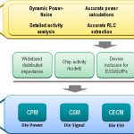
The key to this approach is the generation of various chip abstract models, which are promoted and integrated into the package/system analysis framework. The following two figures illustrate the CPS analysis strategy.
This figure illustrates how the abstracts are incorporated into package/board analysis.
As an example, the power integrity analysis methodology focuses on traditional chip power grid sign-off, including identification of any local switching hotspot issues. A sophisticated RLC model of the chip and package power distribution network is then incorporated into the Chip Package Model (CPM) abstract. The CPM includes pad-level switching currents and capacitances, as well. The “chip-aware” board power distribution analysis incorporates the CPM. Using SiWave, the system designer can now optimize pin assignment, board power plane definition, decoupling capacitor selection and placement, and integration of the voltage regulator module(s).
For signal integrity (and simultaneous switching) analysis, the Chip Signal Model (CSM) abstract is used. The CSM methodology extends the traditional IBIS model approach to include I/O pad ring parasitics, and significantly, the I/O power noise impact on circuit behavior.
For electrostatic discharge reliability analysis, the wafer foundry’s design enablement team will provide ESD design guidelines and related rule checks to IP developers focused on SerDes, memory interface, and general purpose I/O circuits. However, customers may have unique robustness requirements for HBM, MM, and CDM discharge events, outside the characterization range used by the foundry. The Ansys methodology includes generation of the Chip ESD Compact Model (CECM) abstract. Designers can now evaluate ESD protection in a complete system environment model for their application, through the board and package pins.
An analysis methodology that is emerging as crucial to circuit, signal, and system reliability is the thermal profile of the chip-package-system implementation. The importance of accurate thermal modeling is magnified by the increasing use of multiple die-in-package offerings – e.g., 2.5D and 3D designs with various interposer and multi-plane signal redistribution layers. The Chip Thermal Model (CTM) abstract is integrated into the larger Ansys thermal analysis toolset, as illustrated below.
Ansys has continued to expand their CPS methodology, incorporating accurate and detailed chip abstract models into their industry-leading package/board-level tool suites. The synergy between the chip and system tools offers a comprehensive modeling environment, which is absolutely critical for SI, PI, EMI, ESD, and thermal reliability analysis.
There is no longer any doubt that the Apache acquisition belongs in the “win-win” column. For more details on the Ansys/Apache CPS methodology, links to technical papers are available here.
-chipguy