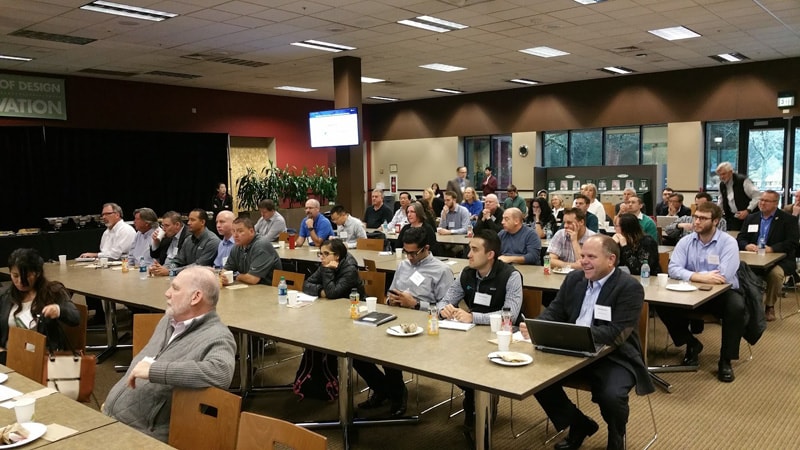
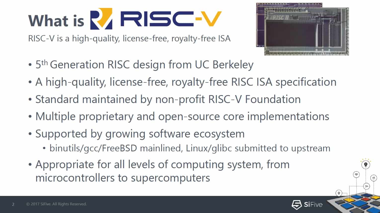
NVM Survey 25 Wide Banner for SemiWiki 800x100 px (1)

Smart & Connected Devices to Artificial Intelligence and Beyond

Smart & Connected Devices to Artificial Intelligence and Beyond
by Daniel Payne on 05-02-2017 at 12:00 pm

Last Friday I attended a breakfast seminar organized by SEMI in Hillsboro, Oregon with fascinating speakers from several high-tech companies: Qorvo, Intel, Oregon Angel Fund, Kimera, Moonshadow Mobile and Yole Development. I recalled that Qorvo was created from the merger of TriQuint Semiconductor and RF Micro Devices back in 2014. Glen Riley fro Qorvo talked about how their RF chips power the 5G and IoT devices through a variety of wireless communication protocols in this $15B RF market. My favorite quote from Glen was about the IoT devices and their sensors, “A sensor without a service is useless”. Think about a Fitbit device for a moment, what makes it valuable is the analysis on health when using analytics.

I could relate to the value of analytics in the cloud for IoT devices as my cycling rides are posted on Strava.com where I can view my GPS maps, compare my times on segments, set goals, analyze heart rate and view my power curve.

Claire Troadec from Yole shared about the RF front-end modules and components for cellphones. She sees emerging markets in Augmented Reality (AR), Virtual Reality (VR), IoT, Smart Cities, wearables and autonomous vehicles. Smartphone growth is slowing, China is driving the highest volumes, Samsung sells more units than Apple, however Apple continues to enjoy higher revenue than Samsung. Comparisons between RF front-end modules showed how varied the engineering approaches are with smart phones today, and I was surprised to see how small the Xiaomi Mi5 boards were.

From Intel we had Dr. Geng Wu talk about 5G technologies and how the market is moving from just Smart Phones into Smart Things like: cars, power grid, trains, virtual reality, drones, smart home, wearables. Intel has a mobile trial platform for mobile devices that uses sub-6/28GHz range and is about the size of a Dime.

Jon Maroney from the Oregon Angel Fund introduced us to three companies:

  • Kimera doing Artificial General Intelligence (AGI) with an algorithm called Nigel based on quantum physics that does unsupervised learning.
  • Moonshadow Mobile has a database engine (DB4IoT) for the Internet of Moving Things.
  • SENRIO does enterprise security for the IoT.


Kimera


Moonshadow


SENRIO

Summary
I learned that our local bus system in Portland called TriMet is using the Moonshadow technology to save on their preventive maintenance and fuel costs for their fleet of buses which are moving IoT devices. The AGI approach used by Kimera is learning how to read, much like a child would, so how far away is the HAL 9000 computer from the famous 2001: A Space Odyssey movie? SENRIO is helping medical equipment companies make their healthcare devices hacker-proof.

My head is still spinning from all of the ideas raised in this breakfast seminar which I thoroughly enjoyed attending, and am looking forward to the next SEMI event here in Oregon.


Scaling Enterprise Potential with ClioSoft’s designHUB platform

Scaling Enterprise Potential with ClioSoft’s designHUB platform
by Mitch Heins on 05-02-2017 at 10:00 am

I’ve had the privilege over the years to be a part of a lot of great companies, teams and projects. Some of these efforts were quite successful while others were not. It begs the question of why is it so hard to enable design reuse and capture the untapped potential of the collective intelligence within our companies? Up till now, companies have had to rely upon tribal knowledge being passed down from the older and wiser employees of the company, but in today’s fast-paced world with ever shifting ranks of employees that is no longer an option.

The reasons for design reuse difficulty are many and varied, but one of the most important is that up till now, we have lacked a good way to capture our shared experiences and reasoning (in whatever endeavor we are under taking) and an easy-to-use way to re-look before we leap at our next endeavor. Perhaps this is about to change. ClioSoft recently announced a new product called designHUB – a platform that not only provides an ecosystem to share IPs but also provides a way to leverage the untapped ideas within the enterprise.

So, what is designHUB? ClioSoft describes designHUB as an extensible platform that enables enterprises to leverage and build on existing design resources within the company. With the notion of design reuse being unique to every company, designHUB has been designed for easy customization and ease of use without having the overhead of a huge CAD team to support it. To realize the concept that untapped ideas, design expertise or any intellectual property can be shared seamlessly across the company and leveraged to produce remarkable results, designHUB has three main components that I’ll endeavor to step through in the following sections.

The first designHUB component is what ClioSoft calls an IP Reuse Ecosystem. For starters, designHUB extends the definition of IPs to not only include the traditional IPs and the IP sub-systems but also include essential design components such as documents, flows, scripts, libraries, etc. which can be shared and reused throughout the enterprise. The IP Reuse Ecosystem is a web-based platform that can either work atop any data management system or be used as a centralized repository to store IPs and design data so that those data can be searched and compared for use in future designs. The key is to store not only IP design data but also IP meta-data (that is data about the data). IP meta-data can be more readily used to give designers information about an IP such as its origin (internal or external), operating specifications, use-model assumptions, licensing restrictions, etc. that can be used to help decide if a given IP is right for the job at hand. The IP Reuse Ecosystem bridges the gap between the IP developers and users enabling a fast resolution to any queries an IP user may have. It gives designers relevant information about whom in the company may have more information about the IP and which designs have used a specific IP in the past. It can also notify designers of any known issues with an IP and any fixes that have been made or that are in the works.

The second designHUB component is what ClioSoft calls the Unified Dashboard & Hub. The dashboard can be thought of as a home-page for designers where they can go to review the notifications or tasks assigned to them or review progress on different design projects in which they are involved. The dashboard is how the designer interacts with the rest of the designHUB to find people, projects, data, and information about IP versioning and timelines. It’s also a place where designers can capture and record discussions and resolutions about their projects, which creates more meta-data for their IP that may eventually be used by future design teams later down the road.

The third designHUB component is known as crowdsourcing. The idea of crowdsourcing in this context is to give designers a way to share and add their insights about anything including IPs to the company’s knowledge base. Crowdsourcing is meant to be an easy way for designers to share information across what would traditionally be company boundaries such as geography, business and functional units. The idea here is that ideas, design expertise and intellectual property can and should be shared easily across a company and leveraged to make the company more productive. Crowdsourcing filters out the barriers to communications giving designers a sense of teamwork even when they aren’t in the same functional unit of the company.

ClioSoft’s designHUB is meant to be design management software agnostic, meaning it can work with any design management software including ClioSoft’s own SOS7 product as well as products such as Git, Subversion, NAS/SAN and others. While designHUB has been designed for usage in the semiconductor industry, the platform is generic in the sense that it could just as easily be used by say a marketing group to manage a company’s marketing collateral, product descriptions, trade-show participation and the like. ClioSoft has also done a nice job of enabling designHUB to being customizable. As an example, designHUB can be interfaced with a variety of business intelligence, data analytics and reporting tools through the inclusion of a REST API. They also have APIs that enable the integration of designHUB with other 3[SUP]rd[/SUP] party systems like bug trackers, DM/SCM systems and the like.

It’s early days for designHUB but I think ClioSoft is on to something here. If they can provide a system that enables companies to methodically capture both data and meta-data for their designs and IPs it’s only a matter of time before some other bright folks will figure out how to apply machine learning and big data analytics to mine this data for more jewels.
See also:

Also Read

Attending DAC in Austin for Free

ClioSoft Crushes it in 2016!

CEO Interview: Srinath Anantharaman of ClioSoft


Webinar – Next Generation DDRM Needs, Solutions

Webinar – Next Generation DDRM Needs, Solutions
by Bernard Murphy on 05-02-2017 at 7:00 am

I’m a believer in product life-cycle management (PLM) for semiconductor design. It’s not an attention-grabbing topic like faster verification or improved PPA in implementation, but now massive IP-based design is routine, IP’s are sourced from multiple suppliers each cycling though multiple revisions and now that design activity is distributed all over the world, not managing the lifecycle tightly is an invitation to disaster.


REGISTER HERE for the Webinar on Thursday, May 18[SUP]th[/SUP] at 8:30am PDT

One particularly important aspect of PLM in the design cycle is Design Data and Release Management (DDRM). Dassault Systemes/Consensia is well-known for its DesignSync solution, a product of long pedigree used extensively at most of the major semis. It provides end-to-end design chain data management for both hardware and software designs and what they call a single source of truth (SSoT) for your entire work-in-progress IP portfolio. And it spans the major design frameworks, including Eclipse and Microsoft Visual Studio for software design and Cadence and Synopsys for digital/custom/analog/AMS design.

Whether you use DesignSync today or not, this webinar should provide you with a valuable update on how leading-edge design teams are pushing DDRM to meet their needs and how they are integrating solutions like this with tooling, including with other DDM repositories.

REGISTER HERE for the Webinar on Thursday, May 18[SUP]th[/SUP] at 8:30am PDT

This webinar, hosted by Consensia, a channel partner of Dassault Systemes, and moderated by Daniel Nenni of SemiWiki.com, will be of interest to anyone involved in AMS or ASIC/SOC design or undertaking system administration for AMS and digital design teams. In this first of a series of webinars on Synchronicity DesignSync, you’ll see how it provides the most comprehensive, scalable and efficient solution for revision control, automated SOC/IP release management and IP management. You’ll learn about the how DesignSync makes multi-site project setup and administration easy and fast, how caching reduces storage and improves designer productivity, how DesignSync is used as an IP management hub to publish SOC Bill of IP, how it manages other DDM repositories, interoperability with other EDA tools and much more. Whether you are an existing DesignSync user or want to find out more about DesignSync, register today for this webinar.


An Overview of Jama Software in the Semiconductor Industry

An Overview of Jama Software in the Semiconductor Industry
by Daniel Payne on 05-01-2017 at 12:00 pm

Portland, Oregon is a hotbed of innovation for software development companies and I tend to scan the headlines of my local newspaper the Oregonian, which is where I first started to read about Jama Software a few years back. Curiosity and opportunity drove me to meet with Trevor Smith of Jama in their Portland office. We chatted for a few hours and I summarized our meeting with the following Q&A interchange to see how they are serving the semiconductor design market to connect requirements across hardware and software teams.

1) When was Jama founded, who was the first customer, and what challenge were they trying to
solve?

A: Jama was founded in 2007 by our Chief Strategy Officer, Eric Winquist, after witnessing first-hand the common frustrations companies face in delivering complex, systems-driven products to market. Teams schooled in a more collaborative, transparent way of working experience road blocks when incorporating outdated technology into their processes and workflows. By providing a solution that brings teams together in a way where they can structure their data to gain meaningful insights around what they are building and why, while incorporating collaborative features that teams desire, Jama Software is bridging the gap between complex systems architecture and design and meaningful collaboration.

2) What industries does Jama serve and why?

A: We have found a strong fit with industries that are either highly regulated, life-, safety-, or economy-critical like Automotive, Medical Devices & Life Sciences, or Aerospace & Defense, or industries that are developing highly complex systems of systems like Consumer or Industrial Technologies, and we’ve seen an especially good fit in the Semiconductor industry where there is a mix of both of those themes: supplying to highly regulated industries (like chips, sensors, etc. for autonomous driving), or complex system design and development like SoCs, FPGAs, etc.

A challenge that we have in the Semiconductor industry is that most teams are working so fast that they typically don’t manage requirements well, if they do it at all, or they don’t see a need to slow down and put a process around their requirements. The benefits we’ve seen in serving the semiconductor market is that by providing teams a platform where they can structure their data to understand and scope the impact of a change, ensure complete test coverage and validation and verification of their requirements because those relationships are visualized, and allowing them a way to track all of the design compromises and conversations that take place around requirements can save them time, help them deliver not only a higher quality product by reducing requirements related defects, but also ensure they are delivering what the customer asked for, and that is something that instills confidence in their customer and can help lead to repeat business, growing their organizations share of that market.

3)What type of engineer would use Jama?

A: Typically systems architects and systems engineers are the ones in the system creating requirements, submitting requirements for review, etc., but also anyone who has a hand in product definition, be it defining a new product and taking that to market, or variants on a previous version of a product – the titles of those folks can vary quite a bit from company to company, but those folks can be on the Marketing or Business side of the house, or on the engineering.

We do, however, see in Semiconductor companies the System Architect (or Systems Engineer) being the ones who benefit greatly from having a solution like Jama – the concept of having a solution that provides full context around what is being built, why it is being built in such a way, and transparency and accountability for those who are demanding that can be a huge time saver because they know exactly who to go to for questions, they can understand the impact of a proposed change, and they can ensure complete coverage all the way through to validation, verification, and test.

4) Who are some of Jama’s competitors and why is Jama different?

There are some requirements management systems out there. A common one for those who have spent time in the Automotive or Aerospace & Defense industries is IBM DOORS. What we hear constantly from our customers & prospects is that with legacy (read outdated) systems like DOORS is that they are just not flexible or configurable enough to the way teams need to structure their data. Hardware and Software teams have different processes they prefer to follow (ie waterfall versus Agile), and Jama allows teams to structure their data and projects in the way that fits them best. In addition, teams want and need a more collaborative structure around requirements definition and review. Lastly, one of the biggest things is the accessibility of the solution. DOORS users consistently complain that you have to be a power user to have any interaction in the tool. With Jama business teams can interact seamlessly via email, engineers working primarily in simulation or CAD tools don’t necessarily want to learn a new tool, but they still want to provide feedback on requirements – Jama allows that interaction to take place without disruption and that has positive impacts across the board – requirements have a higher likelihood of being correct based on the feedback from the broader team, so by the time it gets to the electrical engineer, for example, they have already given feedback and are more likely to satisfy the requirement or specification without the thrash and churn that slows people down.

More common, however, especially in more traditionally fast-moving industries like Semi is that teams are most likely using MS Word and Excel, PowerPoint, and collaborating via email or in person meetings that require a ton of time and overhead.

The biggest problem in using tools like Word and Excel to manage requirements is the manual effort associated with working in those tools. In Michael Kennedy’s book Product Development for the Lean Enterprise he talks about Toyota and the fact that their engineers spend 80% of their time on engineering while suggesting that at Western companies it may be the opposite and engineers may be spending only 20% of their time on engineering tasks. Given that we have helped move so many companies from a document-based process to a web-based process, this doesn’t surprise me one bit. The amount of time spent reconciling requirements documents to avoid disparity in requirements versions, manually updating traceability relationships and requirements test coverage for compliance, not to mention reviewing requirements documents, is astonishing, but most people don’t know there is another way, a more automated solution, and that is where Jama Software comes in.

5) Why do semiconductor companies use Jama?

We have found that there are 2 major challenges facing the semiconductor market. The first is the complexity of the products being produced is increasing at an incredibly rapid pace. Companies are forced to add more functionality and include software with the solutions they are providing. This increase in complexity means semiconductor companies must find a way to ensure they are building product customers want and at the right time. We have found that Jama allows our customers to keep track of the customer’s requirements, collaborate on tradeoffs with the engineering teams and track those requirements all the way through verification. It is no longer sufficient to write an MRD or a PRD and load it somewhere in Sharepoint, the requirements and specifications must be tracked and connected to each other in a system like Jama. Jama allows our customers to reduce the number of tape outs at the end of a project because the engineering teams have a database that allows them to view and discuss the requirements and specifications in real time.

The second challenge relates to new market opportunities. The explosion of interest in technology like automated driving and the automotive space as a whole has led numerous semiconductor companies to begin developing products for these regulated markets. Automotive regulations like ISO 26262 require companies to be able to demonstrate the traceability of these products requirements. Jama has done an extensive amount of work with regulated customers incuding an audit of the tool itself to be fit for purpose for companies building products for the automotive segments. By using Jama our customers have the necessary tools to unlock the revenues and profits from these regulated markets.

Our customers realize more return on their engineering investment by allowing engineers to focus on building great products and not focus on unnecessary searching. We also have experts who come from the semiconductor industry who provide the best practices of product development to increase the adoption of Jama within the companies who have selected us. This commitment to improving the product development process specifically for customers in the semiconductor market helps every one of the companies we work with.

6) What should I do to find out more about Jama?

Please visit our websiteor you can contact us here.

There is also an option to try Jama Software for free for 30 days.

We are also hosting a webinar with Methodics on April 27[SUP]th[/SUP], discussing the benefits and business value of connecting Requirements to IP. We will also show how Methodics and Jama Software are working together to solve that challenge.


SEMICON Southeast Asia reflects strong equipment market

SEMICON Southeast Asia reflects strong equipment market
by Bill Jewell on 04-28-2017 at 4:00 pm

SEMICON Southeast Asia was held this week in Penang, Malaysia. Over 6500 people attended the conference to learn about the latest trends and equipment in semiconductor manufacturing.


Dr. Dan Tracy, Senior Director Industry Research and Statistics at SEMI, presented an optimistic outlook for the semiconductor equipment market in 2017. Semiconductor capital spending (cap ex) and semiconductor manufacturing equipment spending are both expected to show double digit growth, with cap ex at 10.9% and equipment at 12.2%.

[TABLE] border=”1″ align=”center”
|-
| colspan=”4″ style=”width: 480px” |

Semiconductor Capital Spending & Manufacturing Equipment Forecast
Annual Change, Source: SEMI April 2017

|-
| style=”width: 120px” |
| style=”width: 120px; text-align: center” | 2015
| style=”width: 120px; text-align: center” | 2016
| style=”width: 120px; text-align: center” | 2017
|-
| style=”width: 120px” | Cap Ex
| style=”width: 120px; text-align: center” | -0.5%
| style=”width: 120px; text-align: center” | 3.8%
| style=”width: 120px; text-align: center” | 10.9%
|-
| style=”width: 120px” | Equipment
| style=”width: 120px; text-align: center” | -2.6%
| style=”width: 120px; text-align: center” | 12.9%
| style=”width: 120px; text-align: center” | 12.2%
|-

The strong growth is driven by key semiconductor applications: storage, industrial, wireless, automotive and consumer. The strongest growth in semiconductor products will be in memory (up 15% to 20%) and sensors (up 9% to 11%).

China will be the major source of growth in semiconductor manufacturing over the next few years according to Clark Tseng, senior research manager of SEMI Taiwan. China has 20 new wafer fabs started or planned from 2016 to 2019 and is expected to account for 20% of global wafer fab capacity by 2020. Foreign companies have accounted for the majority of wafer fab spending in China, but Chinese companies should account for the majority of spending by 2018. China should be the largest market for wafer fab equipment by 2019 or 2020.

Lung Chu, president of SEMI China, discussed the Chinese government’s commitment of about US$75 billion to expand the semiconductor industry in China. The key reasons China wishes to expand its semiconductor industry are:

· Reduce the annual semiconductor trade deficit of over $160 billion, the largest for any product category including oil.

· Ensure domestic production of semiconductors needed for national security

· Increase participation in the industry driving innovation in electronics.

According to Lung Chu, China has some hurdles to overcome to catch up to the rest of the world. China fabless semiconductor companies are weak in microprocessors, microcontrollers, FPGAs, DSPs and memory. Chinese foundries are about two generations behind the major foundries in process technology.

SEMI’s optimism semiconductor manufacturing equipment growth in 2017 supported by the combined shipment data from SEMI and SEAJ. 1[SUP]st[/SUP]quarter 2017 shipments were $10,360 million, up 14% from 4Q 2016 and up 57% from a year ago. SEMI discontinued bookings data in December 2016, when the book-to-bill ratio was 1.06. SEAJ’s book-to-bill ratio in March 2017 was 1.12. We at Semiconductor Intelligence are projecting full year 2017 equipment growth will be in the 30% to 40% range.


The $10 billion quarterly level for semiconductor manufacturing equipment has not be reached since the boom year of 2000. The five quarters of consecutive quarter-to-quarter growth has also not been seen since 2000, except for the 2[SUP]nd[/SUP] half 2009 to 2010 recovery from the 2008 to 1[SUP]st[/SUP] half 2009 downturn.

Is the current boom in semiconductor manufacturing equipment driven by real need for additional capacity or could the industry be headed for overcapacity? It is too early to tell; however, the 2017 capital spending plans of major semiconductor companies provide a clue. IC Insights in March projected total cap ex in 2017 of $72.3 billion, up 6% from 2016. The top ten spenders account for 77% of the total.

[TABLE] border=”1″ align=”center”
|-
| colspan=”5″ style=”width: 514px; text-align: center” | 2017 Capital Spending Forecast, US$B
|-
| colspan=”5″ style=”width: 514px; text-align: center” | Sources: IC Insights, March 2017; Semiconductor Intelligence, April 2017
|-
| style=”width: 103px; text-align: center” |
| style=”width: 103px; text-align: center” | 2016
| style=”width: 103px; text-align: center” | 2017
| style=”width: 103px; text-align: center” | Change, $B
| style=”width: 103px; text-align: center” | % Change
|-
| style=”width: 103px” | Memory
| style=”width: 103px; text-align: center” | 25.8
| style=”width: 103px; text-align: center” | 27.2
| style=”width: 103px; text-align: center” | 1.4
| style=”width: 103px; text-align: center” | 5.3%
|-
| style=”width: 103px” | Foundry
| style=”width: 103px; text-align: center” | 17.2
| style=”width: 103px; text-align: center” | 16.3
| style=”width: 103px; text-align: center” | (0.9)
| style=”width: 103px; text-align: center” | -5.3%
|-
| style=”width: 103px” | Intel
| style=”width: 103px; text-align: center” | 9.6
| style=”width: 103px; text-align: center” | 12.0
| style=”width: 103px; text-align: center” | 2.4
| style=”width: 103px; text-align: center” | 25%
|-
| style=”width: 103px” | Others
| style=”width: 103px; text-align: center” | 15.3
| style=”width: 103px; text-align: center” | 16.8
| style=”width: 103px; text-align: center” | 1.5
| style=”width: 103px; text-align: center” | 9.8%
|-
| style=”width: 103px” | Total
| style=”width: 103px; text-align: center” | 68.0
| style=”width: 103px; text-align: center” | 72.3
| style=”width: 103px; text-align: center” | 4.3
| style=”width: 103px; text-align: center” | 6.4%
|-
| colspan=”5″ style=”width: 514px” |
|-
| colspan=”5″ style=”width: 514px” | Memory: Samsung, SK Hynix, Micron, Toshiba, SanDisk/Western Digital
|-
| colspan=”5″ style=”width: 514px” | Foundry: TSMC, SMIC, UMC, GlobalFoundries
|-

Based on the IC Insights data, we have grouped the top ten spenders by category. The memory companies combined plan a $1.4 billion increase in cap ex, up 5.3%. The foundry companies plan a $0.9 billion decrease, down 5.3%. Intel plans a $2.4 billion increase, up 25%. Intel is in a unique situation, with few significant competitors for its major microprocessor products. The memory companies sell primarily commodity products into a market which is currently booming, with prices almost double a year ago. The foundry companies generally base their capacity plans on the projections provided by their customers. The foundry customers largely sell application specific products and are in close communication with their end customers in their targeted segments.

Thus capital spending growth in 2017 should be largely driven by the memory companies in the middle of a booming commodity market. The foundry companies, arguably closer to the true capacity needs of their customers, are cutting spending. Plans will change over the course of the year. We expect many companies will reduce their planned spending, especially the memory companies. If the current growth in the semiconductor equipment market is based largely on speculation rather than solid demand, we could see a significant correction in 2018 or 2019.


SPIE 2017 – imec papers and interview

SPIE 2017 – imec papers and interview
by Scotten Jones on 04-28-2017 at 12:00 pm

At the SPIE Advanced Lithography Conference imec published a number of papers on EUV, multi-patterning and other lithography issues. In addition to seeing several of the papers presented I had a chance to sit down with imec’s director of advanced patterning, Greg McIntyre. In this article I will summarize my discussions with Greg and some of the key message from the imec work.

When we first sat down I told Greg I was surprised that neither Intel or Samsung mentioned Line Width Roughness (LWR) in their EUV readiness talks. Greg said that for the foundry N7 – 40nm metal pitches that vias can be printed with the materials available today and that the roughness is OK. He did note that further improvement would be required for 5nm.

We then talked about different imec papers from the conference.

Self-Aligned Block Technology: A Step Towards Further Scaling
Ass multi-patterning has evolved to produce smaller features the number of cut/block masks has been growing leading to Edge Placement Error (EPE) issues. By using materials with differences in etch rates Self-Aligned Blocks (SAB) can be created mitigating EPE. Figure 1 illustrates the basic concept. The masks for the SAB approach always come in pairs so it could be a mask reduction technique for immersion but not for EUV. Specifically, metal oxides were investigated as a material to fill between spacers for Self-Aligned multi-patterning. SAB is a promising technology for insertion at the imec 5nm node.


Figure 1. Self Aligned Block.

SAQP & EUV Block patterning of BEoL metal layers on imec’s iN7 platform
The imec iN7 node has a metal 1 (M1) pitch of 42nm to match the contacted poly pitch and a metal 2 (M2) pitch of 32nm. Both M1 and M2 are unidirectional with self-aligned via 1 on a 42nm pitch connecting M2 to M1. M1 and V1 can both be created with single EUV exposures. For M2 single exposure EUV is challenging to meet a 21nm Tip To Tip (T2T). For M2 with immersion Self Aligned Quadruple Patterning (SAQP) with 4 to 5 masks is required. The number of masks makes overlay challenging and drive process complexity. SAQP with a single EUV block mask is promising. The photoresist needs to get a little better for blocks but there are knobs to address it. Figure 2 summaries the trade-offs of EUV single exposure, SAQP with immersion blocks and SAQP with EUV block.

Figure 2. EUV Versus SAQP and Block.

Novel Membrane Solutions for EUV Pellicle: Better or Not?
In my SPIE 2017: EUV Readiness for High Volume Manufacturing article I discussed the need for pellicles for EUV. The current approach to pellicles uses polysilicon but there are concerns about the scalability of polysilicon to higher power EUV light sources. A successful EUV pellicle needs to have high transmission of EUV light, be mechanically strong, thermally stable and stand up hydrogen exposure. Carbon Nano Tube (CNT) materials have good EUV transmission and mechanical and thermal properties, however, hydrogen attacks the material. With a coating to protect against hydrogen attack CNT looks promising as a pellicle material.

You can read my EUV High Volume Manufacturing Readiness article here.

Exploration of a Low-Temperature PEALD Technology to Trim and Smooth 193i Photoresist
LWR is a major challenge for EUV and even immersion lithography as we move to the iN5 node and beyond. Plasma Enhanced Atomic Layer Deposition (PEALD) was investigated as a trim and smoothing option. For trimming various chemistries and powers were investigated. High power O2/Ar reduces the vertical height of the photoresist faster than the lateral width. O2/N2 low power chemistry can trim laterally while preserving the photoresist height. H2/Ar provide some trimming but saturate quickly, pure Ar doesn’t provide any trimming. All of the chemistries provide some line smoothing with H2/Ar providing the best smoothing.

Low Track Height Standard cell Design in iN7 using Scaling Boosters
The size of standard cells used in logic designs is determined by the Minimum Metal Pitch (MMP) multiplied by the track height multiplied by the Contacted Poly Pitch (CPP). With the difficulties being experience with scaling MMP and CPP track height has become an increasingly important factor in scaling. The problem with track height scaling is that as the number of tracks shrinks the number of fins per transistor is also reduced and without optimization the cell performance is degraded. In this paper, a 7.5-track cell is achieved by adding a Middle Of Line (MOL) layers for layout optimization, for a 6.5-track cell a fully self-aligned gate contact is added and finally a buried rail is used to achieve a 6-track cell. The 6-track cell is a full 45% smaller than the 7.5-track cell.

Single Exposure EUV Patterning of BEOL Metal Layers On The IMEC iN7 Platform

The imec N7 (iN7) or foundry 5nm (F5) node has a 42nm M1 pitch with 24nm T2T, Via is 21nm x 32nm with a 42nm pitch and M2 is a 32nm pitch with 25nm T2T. Options for M1 are SADP with EUV block or single EUV exposure, via is single exposure EUV and M2 options are SAQP with EUV block or single exposure EUV. Figure 3 summarizes the advantages and challenges of single exposure EUV.

Figure 3. EUV trade-offs for Metal layers.

Single exposure EUV with litho and etch co-optimization can meet the needs of 1D M1 metal. For M2 single exposure can be used for gridded designs at 32nm pitch but further optimization is needed on logic designs.

EUV Final Thoughts
Greg had a few final thoughts on EUV.

  • EUV pellicles – CNT and coated, you can inspect through them with 193 inspection tools They are ramping up manufacturing now.
  • They are working on alternate absorbers for reticles. Going to nickel or cobalt can make the absorbers much thinner reducing 3D effects. The current reticles are OK for N7 and N5 but will need to be improved for N3.


Directed Self Assembly (DSA)

I told Greg I thought there was less interest in DSA at the conference and he said DSA momentum is down. He did note the following:

  • Defectivity is down – he thinks the chip – chemo epitaxial process has the potential to be used for memory.
  • DSA is also being looked at to “heal” roughness for EUV.
  • Also materials that pull apart more are being looked at to get below 20nm.

EDA CEO Outlook 2017

EDA CEO Outlook 2017
by Daniel Nenni on 04-28-2017 at 7:00 am

A long standing tradition has returned to EDA: The CEO Outlook sponsored by ESDA (formerly EDAC) which alone is worth the price of membership! Not only do you get a free meal, the event included quality networking time with the semiconductor elite. In the past, financial analysts moderated this event holding the CEO’s feet to the fire. Let’s hope that tradition returns next year because that is excellent content.

This year was especially interesting because two of the four CEOs sold their companies to much larger entities last year and you could tell because of the relaxed looks on their faces and less guarded responses to questions. There was also some interesting acquisition chatter that could be EDA disruptive and that was about Imagination Technologies and the Calibre unit of Mentor. Synopsys and Cadence both have unique opportunities here so it will be interesting to see who comes out on top.

Security was the most discussed topic of the night with ARM CEO Simon Segar, Synopsys CEO Aart de Gues, Cadence CEO Lip-Bu Tan, and Mentor Siemens CEO Wally Rhines all making some important points. Simon is not satisfied with security progress citing time to market as much more of a priority than shipping a secure product. ARM has invested heavily in security making it one of the three pillars of SoC design: Low power, high performance, and security. Aart noted that systems companies are asking chip companies for security guarantees which of course will not happen. To me this is even more reason for fabless systems companies to take control over their silicon as Apple has done. Aart also talked about “secure by construction” and the need for security regulation. Wally also talked about customers driving chip security and being willing to pay for it because today there is security technology that is not being fully utilized. Lip-Bu also talked about working with systems companies on being more willing and able to implement security in their chips.

Semiconductor IP was also discussed with Lip-Bu mentioning that IP outsourcing is growing which brings us to Imagination Technologies. As the story goes, Apple tried to buy Imagination last year but the perceived value, as a result of the ARM acquisition, was ridiculously high so Apple decided to develop their own GPU. Given that Apple is responsible for 48% of Imagination’s revenue their market value dropped more than 75%. Clearly Imagination Technologies will be a shell of the company they once were without Apple so to me an acquisition is imminent. Other than QCOM (for a patent play), my two leading candidates to acquire imagination are Cadence and Synopsys. Cadence has a new IP VP who needs to revitalize their IP business and has no overlap with Imagination products. Synopsys has overlap but they are the IP leader due to some very clever acquisitions. Both companies would benefit from helping Apple avoid any legal complications of developing their own GPU after being intimate with Imagination and even hiring some of their designers. Apple is a big EDA, IP, and emulation customer so a little Apple goodwill can generate a lot of revenue.

The other interesting conversation over beer and some very tasty food was the Mentor Calibre unit. From what I understand, verification is not essential to the Siemens corporate strategy and a bidding war between Synopsys and Cadence could result in a multi-billion dollar windfall.

Given those two ripe acquisition opportunities I see EDA as having another big year, absolutely.

You can see pictures and a video of the event here. It was an uncharacteristically wet and stormy night in Northern California so the people who attended, myself included, really wanted to be there.

2017 CEO Outlook

Four industry CEOs discuss their views of the industry’s future
Thursday, April 6, 2017, 6:30pm – 8:45pm, at Synopsys, Mountain View, California


IoT in the Cloud with Microsoft and Mentor

IoT in the Cloud with Microsoft and Mentor
by Daniel Payne on 04-27-2017 at 12:00 pm

I cycle for fitness five days per week and use the Strava.com site to post my rides, analyze the ride data and chat with other cyclists, however in February this year the Amazon Web Services went down which crashed Strava, making me sad and nervous at the same time. Of course, there are alternatives to Amazon Web Services and the engineers at Microsoft have their own cloud services called Microsoft Azure, used in 90% of Fortune 500 companies. I just learned that the embedded systems division at Mentor Graphics has joined the Microsoft Azure Certified for IoT.

Unlike other EDA companies, Mentor has been in the embedded systems business for a few decades now and they have a couple of OS choices based on the type of IoT system that you’re building:

  • Nucleus RTOS
  • Yocto Project-based Embedded Linux

So if you’re building an IoT project and need to analyze all of that sensor data by accessing it in the cloud, how do you pull all of that technology together? Instead of cobbling together something from scratch which would take a long time and require specialized engineering talent, you can now consider using pre-verified technology from trusted companies that have the engineering resources to make this process much simpler for your team. Mentor has taken the Azure SDK and integrated it for you into their Nucleus and Linux platforms.

Who else is part of this Azure Certified IoTprogram? Well, scores of companies that you probably have heard of before, like: Intel, RaspberryPi, Freescale, TI, Dell, HP, Arrow, ST, Fujitsu, Hitachi, Toshiba, Ricoh, Renesas. Mentor is in good company by joining with Microsoft Azure. You can get more details about Mentor’s integration with Microsoft Azure by watching a 17 minutes archived webinar. Shown in light blue below are the two specific integration pieces that Mentor has added: Azure Device SDK, Azure Gateway SDK. The parts shown in dark blue are existing Mentor products from the embedded systems group.

The Mentor webinar covers the IoT marketplace, growth projections, objections to adoption, vertical markets and cloud infrastructure vendors. Mentor’s IoT approach uses both cloud services and embedded devices that connect with Microsoft Azure:

Users of Microsoft Azure get dozens of services to help analyze their IoT data:

Consider an industrial IoT example with sensors, actuators, controllers, factory network, cloud services and a mobile app:


The actuators and sensors shown on the left get connected securely using the Azure device SDK, the controllers read the sensor data and then control factory equipment using a secure gateway that is Azure-enabled. Android devices can run apps to help the factory workers and managers visualize what is happening inside of their factory and ensure efficient operations. With Mentor’s embedded edge device view you can cloud-enable an IoT device to Microsoft Azure with device services like:

  • Device discovery
  • Device provisioning
  • Device management
  • Configuration
  • Device to cloud messaging
  • Cloud to device messaging
  • Bulk upload or download
  • Alarms and events
  • Firmware updates
  • Device restart

Related blog – The deep blue, I mean, the deep Azure sky before me

Using gateway enablement you get all of the previous list of device services plus:

  • Data aggregation
  • Filtering
  • Protocol mapping, translation
  • Micro services
  • Message broker services

This sounds promising, but what about security using Mentor and Microsoft Azure Cloud? Good news here as Mentor’s security technology is used to secure data in rest, data in use and date in motion. This security includes:

  • Hardware root of trust
  • Wurldtech Certification
  • Encryption, Crypto libraries
  • ARM TrustZone
  • CVE, US-DERT monitoring

Related blog – Writing about the cloud while in the clouds

Summary
The IoT opportunities for businesses are growing by leaps and bounds, limited only by imagination, engineering talent and budgeting. What Mentor’s integration with the Microsoft Azure Cloud brings to the IoT community is support for both gateway and edge device configurations, pre-integration and testing with Microsoft Azure SDKs, embedded and cloud services, and finally security. In the typical engineering world of make versus buy decisions, I would certainly give the Mentor and Microsoft combination a closer look before attempting to make my own integration from scratch.


Lip-Bu on Opportunity

Lip-Bu on Opportunity
by Bernard Murphy on 04-27-2017 at 7:00 am

Given a chance to talk with someone as connected as Lip-Bu Tan (President and CEO of Cadence and Chairman of the VC firm Walden International), it is tempting to ask all the usual questions about industry growth and directions in cloud, automotive, IIoT, AI and so on. I wanted to try something different. If you make a living (or plan to) in semiconductor design and EDA, this explosion of new technologies makes for interesting reading, but what does it mean for your job? Since all the press seems to be around the mega-companies in these fields (Google, et al), why not look for jobs there, especially given their supposedly stratospheric salaries and the chance to work with bleeding-edge technology?


Lip-Bu acknowledged that superficially it is difficult to compete for talent with these giants. But he made the point that most engineers want to solve difficult problems, and they want to have an impact. The big companies offer the first (if you can make it through the selection process), but not so much of the second. However, thanks to all those new emerging technologies, new problems and opportunities are sprouting like weeds in EDA. And solutions are starting to leverage leading-edge technologies in machine learning, big data analytics, neural nets and cloud-friendly development and deployment. Engineers working in these areas get to work on big hairy problems and learn about and use the latest development platforms.

Lip-Bu pointed to a few big drivers for this change. He mentioned first that a lot more business is now coming from systems companies (representing 40% of revenue for Cadence). Those companies are motivated to get maximum value from partners by offloading as many requirements for expertise as they can. Since what the systems companies are doing is ground-breaking, they expect more collaborative innovation from their partners leveraging state-of-the-art methods like machine-learning where the traditional EDA customer-base might prefer to keep that learning and expertise in-house.

Another interesting driver here in an increasing appreciation for the value of data. Companies like Cadence have incredibly rich stores of data on the architecting, verification and implementation of countless designs across all possible domains. Machine learning techniques can potentially be applied to improve results with specific types of designs like an IP block, for instance, enabling teams to focus more on the big objectives and less on the minutiae so they can get to market faster. Systems companies recognize this advantage and want to tap into it.

Lip-Bu next made a point about why this has become so important and drew an interesting analogy between the pharmaceutical industry and design/EDA. Big pharma traditionally focused on blockbuster drugs—spending a lot of money to develop and test a drug that you could sell to millions. That business model still works, but the real growth is in personalized medicine; cancer treatment is one area where tailored medication looks much more successful than blockbuster approaches. The same trend seems to be happening in design. When you look at the IoT, recognition, differentiation in the cloud, all these areas are driving similar “personalization” by applications in hardware design because it has become clear that customized solutions can get not just a little edge but orders of magnitude advantage over traditional solutions.

That means a lot more designs must be turned a lot more quickly by teams who want to (quickly) deliver the best possible solution for their application, but those teams, in many cases, have no interest in delivering to markets beyond their internal needs. So there’s a big hairy problem – deliver methods to build bigger, faster, lower-power designs but much more quickly and efficiently than can be done today, using a lot more intelligence tapped from that massive database of prior experience.

Lip-Bu stressed several times that Cadence is very much in learning mode with its partners on their needs, but it’s clear to me that they are not waiting to be told exactly what to do. As they learn, they are already aggressively building capability around machine learning, around massive parallelization in the cloud and around a host of other cool solutions to big hairy problems in a wide range of application areas, which I don’t have space to cover here.

So, when you think about whether you want to work for a company like Cadence or a company like Google, consider this. With the big guys, forget about the superstar salaries unless you’re already world-famous. You might still make (some) more money, but you’ll be buried in a giant team where your contribution will be relatively small. Or, you could work in an EDA company where there are lots of hard problems, innovation is essential and you can be a major contributor to an important solution. You can still wax poetic about how what you do makes the rest of this new industrial revolution possible. But it’s nice to be recognized for what you have done too, and it doesn’t hurt your career prospects to know you’re developing skills at the leading edge, just like the big guys.


Approaches for EM, IR and Thermal Analysis of ICs

Approaches for EM, IR and Thermal Analysis of ICs
by Daniel Payne on 04-26-2017 at 12:10 pm

As an engineer I’ve learned how to trade off using various EDA tools based on the accuracy requirements and the time available to complete a project. EDA vendors have been offering software tools to help us with reliability concerns like EM, IR drop and thermal analysis for several years now. Last week I attended a webinar from Silvaco that discussed how they have two approaches in this analysis area:

  • Highest accuracy tool, used by circuit designers for sign-off – InVar
  • Fastest run times, used by layout designers before design is LVS clean – InVar Prime

The InVar tools were part of an acquisition that Silvaco did of Invarian back in 2015, so it’s always a positive sign when the acquired product line continues to grow into new markets. With InVar Prime the tool user is the layout designer that wants to check out the quality of the routing and interconnect early on in the design process, even before the design is LVS clean. At such an early stage you can quickly pinpoint and fix the layout issues.

One technique to get fastest runs times for this type of analysis is to avoid using a SPICE circuit simulator, and instead use an approach with user-provided current source values. Here’s an overview of how this type of modeling works with an extracted IC layout:

A layout engineer can analyze the power and ground network for quality, estimate the IR drops, estimate current densities, look at point to point resistance values, uncover missing vias, find narrow wires and even uncover detour power routing. All of this early analysis will help meet the tape-out schedule and reduce costly design iterations.

So what does a user of InVar Prime have to supply the tool as inputs?

  • GDSII or Open Access
  • Technology file (ITF or iRCX)
  • Current source info (from a GUI, script or SPICE results)
  • Voltage source info

The capacity of InVar Prime is extended through the use of hierarchy, where each sub-block can be analyzed first before looking at the entire chip. Analysis speeds are quite fast, which allow the layout engineer to get multiple runs per day. Feedback from the analysis is both visually and textual, so for IR drop analysis you can see the regions of greatest drop in the color Red, or click on the text report to pinpoint the areas of greatest voltage drop:

Using an example standard cell layout they introduced an error by removing vias in the power net at the lower-left corner, then ran the IR drop analysis to quickly show the regions of highest voltage drop:

For EM and current density analysis your design can have any number of supply nets and you can see the regions of highest current density using the familiar rainbow of colors, review textual reports, or even click on a text report and view the graphical region. Scripting with the Tcl language can also be used to make your analysis even more automated.

If you need to find where the greatest resistance is from the source of one point in your power network to its final destination then the analysis results are presented both visually and in text formats.

As an IC operates then each transistor produces heat based on the device sizes, currents, frequency and quality of the power and ground networks. The InVar Prime tool provides thermal analysis in either 2D or 3D modes.

It’s interesting to compare the faster speed of using InVar Prime (gold) versus the SPICE-based InVar tool on three different designs:

With InVar Prime the run times are faster, use less RAM and take less time to prepare the analysis.

Summary
IR, EM and thermal analysis are key to ensuring that your chip designs perform reliably and correctly in first silicon, so now you have two approaches from Silvaco with their InVar and InVar Prime tools. The InVar tool was introduced back in 2010 while the InVar Prime tool was introduced 12 months ago, and they have happy customers that have designed processors, displays, memories, high current IC, sensors, mobile, WiFi networks and wired network chips.

To view the archived webinar, watch it online.