webinar banner AI 2026 v2

The Technology China Trade Growing Snowball

The Technology China Trade Growing Snowball
by Robert Maire on 06-28-2018 at 12:00 pm

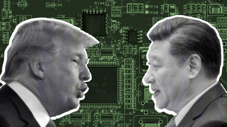
As we have been warning for months the China trade issue continues to grow and accelerate. As we are approaching the June 30th cliff (when export sanctions will be announced) it seems as if the administration has given the industry a kick so we fly even further. The US will also restrict Chinese investment in US tech companies. The administration went on to say that other foreign countries beyond China will also be held to the same restrictions.

Ir seems fairly clear that China’s “Made in China 2025” program is a red flag to the current US administration. Given this further escalation , it makes it even harder to back down from the edge that we are racing towards. We had previously said that a resolution prior to the June 30th announcement was low, we now put the odds at less than zero.

Even if we backed off or found a way to settle with China, we think permanent damage has been done to the tech industry that will either take very long to recover from or never recover at all. The repercussions are much broader after you realize all the interconnectedness of the Chinese and US economies.

We may also be helping other countries compete against us on the global stage given our. It’s very difficult if not impossible to calculate the full risk of semiconductor trade with China as there are many derivatives that are unclear. Much of this will also remain unclear as even after the June 30th list comes out we are sure there will be questions.

A very rough guess of 25% of the overall US semiconductor industry may be a starting point. At least 15% or so of the semi equipment industry is likely at risk. The risk obviously varies widely. The stocks will be driven primarily by this China trade issue as there are limited other drivers at this point. The stocks have done well and are well priced which can set us up for downside.

Throwing a wet blanket on M&A?
We can well imagine that we might see a slight slow down in semiconductor M&A or at least an easing of valuations assuming China will be taken out of the bidding process. China has a very big $100B checkbook for the semiconductor industry and if we stop them from bidding we could see reduced M&A activity and at the very least lower valuations as a bidder with money burning a hole in their pocket has been thrown out of the game.

Companies who may have embraced one another with fear of being acquired may be OK being single and boards may not see dollar signs of big Chinese checks.

Helping foreign competitors in China
By refusing to sell to China we will cede the Chinese market to our competitors plain and simple. While not selling them oil and pork bellies is easily replaced by other countries in a commodity market chips and chip equipment is not quite a commodity in many cases.

In semiconductor equipment both Lam and AMAT compete against the likes of Tokyo Electron (who AMAT tried to buy) as well as Hitachi. They both also compete against ASM International (not ASML). KLA , NANO and Rudolph have NOVA (of Israel) as a competitor as well as Hitachi and others. Veeco has Aixtron in Germany. You also have indigenous Chinese suppliers like AMEC.

You can be sure that salesmen at Tokyo Electron , Hitachi, Nova, AMEC and Aixtron and others have already placed calls to their Chinese customers to offer help against those untrustworthy Americans. We have seen the trailer for this movie before in the Veeco/AMEC dust up in China. We think Veeco permanently lost customers who would rather buy from a local supplier, AMEC, rather than a US supplier who could be cut off at any minute even if the technology was worse and price higher. Its more important to have a steady supply to stay in business as ZTE found out.

Even if we kiss and make up with China, as Veeco and AMEC did, the damage has already been done and is “undoable”.

“Billing” address versus “ship to” address?Moody’s gets it wrong…
We found a laughable news report that Moody’s (obviously experts in the semiconductor equipment industry) that said that China will have a limited impact on the semiconductor equipment industry as “indigenous” business with China amounts to only 6% of AMAT, LRCX & KLAC.

We don’t think even the current administration with its limited understanding of tech thinks for a second that technology loss to China only matters with companies that are “indigenous” to China (ie; billing address is in China).

The issue is that companies like Intel, Samsung and others are building fabs in China and teaching them. This is much like Japanese engineers who on their weekend breaks flew to Korea to help set up Korea in the semiconductor business.

What Moody’s got wrong is that it is the “ship to” address that matters and that is a lot, lot larger than 6%….more like 15% or more. China is the fastest growing market for semiconductor equipment period. With memory slowing its even more important than ever.

Who cares who pays for it or gets the bill or where the company is headquartered, what matters is what equipment shows up inside China, thats what the administration wants to stop and they are not so stupid as to use a “bill to” address.

This means that life for companies like Intel and Samsung will get very complicated. Will they abide by restrictions which could put their China operations out of business? Will equipment be “trans-shipped” from Korea and Oregon? Will equipment makers service “gray market” equipment? Will they be breaking the law? Will they just buy from non US equipment companies for their China operations and teach the Chinese how to make do?

It going to get very ugly, very confusing and very messy.

US semi equipment manufacturing in China at risk?
One thing not widely mentioned are equipment companies that manufacture in China and ship back to the US. Two companies that come to mind are AEIS which moved its semiconductor power supply manufacturing from Colorado to China a long time ago and UCTT which makes a significant amount of its product in China and has been one of the leaders in outsourcing to China.

What will the tariffs do to those products? what could the impact on gross margins be? These products go into AMAT and Lam tools which could in turn be at risk.

Ignoring the 800 pound gorilla in the room….China trade
We find it interesting that quite a few so called analysts have not mentioned China trade as an issue or mentioned it only in passing. We have published numerous articles starting with our April first issue warning of a potential equipment embargo and reporting on the increasing issues and associated risks. We similarly started ringing alarm bells about the dependence on memory growing to an unsustainable level of business. Other analysts only recognized the memory market issues after Samsung stopped its orders.

We pointed out in our last newsletter that both memory and China have been the two brightest spots in the industry and now both have dimmed at the same time for different reasons. It seems that many have not fully calculated the potential impact of China and will only do so after the fact on July 1st.

Investors need to pay attention as headline risk can cause stocks to go down in the near term even if trade issues are worked out over the longer term

The Stocks….
We had mentioned in the past weeks to our clients that being short the semi group would probably be appropriate going into June 15th and June 30th and so far that seems to be the case.

We would mention again to investors that a simple way to be short the group is SOXS (not SOXX). SOXS is a 3X bear index of the SOXX index. The SOXX was down 3.13% today while SOXS was up 8.7% today. At the very least, for those long term holders who don’t want to trade out of positions and go short you can “hedge” your bets a bit with SOXS (we have no affiliation and get no compensation…).

We made some money in AMAT’s quarter suggesting it had downside to a”4″ handle, and it was down 10%. We thought $45 might be a good place to buy in again but we are re-thinking that in light of the worsening Chinese trade issues.

When investors see a 25% shipments down quarter from Lam we could see a $150ish price. KLAC has been immune until recently but has still been holding up relatively well. ASML has broken below $200 which we view as an important psychological barrier.

Unfortunately we see no positive news coming out before the June 30th “D” day for exports to China and don’t think Semicon will help the stocks either. Even good numbers from Micron haven’t helped much and Intel’s CEO issues don’t help either….

All is not quiet on the semiconductor front and the war is going poorly before it even starts…


Design for Power: An Insider View

Design for Power: An Insider View
by Bernard Murphy on 06-28-2018 at 7:00 am

The second keynote at Mentor’s U2U this year was given by Hooman Moshar, VP of Engineering at Broadcom, on the always (these days) important topic of design for power. This is one of my favorite areas. I have, I think, a decent theoretical background in the topic, but I definitely need a periodic refresh on the ground reality from the people who are actually designing these devices. Hooman provided a lot of insight in this keynote.


He set the stage by defining categories for power. Category 1 is high end, high performance, high margin where power is managed as needed at any cost. Category 2 is mid-range, good performance but under margin pressure, where power is critical to system cost. Category 3 is low end, lower performance and low margin where power is critical to system operation (e.g. battery/system lifetime). In his talk, Hooman focused mostly on Category 2 devices. He covered a lot of background on power and the challenges, which I won’t try to cover in depth here; just a few areas that particularly struck me.

First, some general system observations. He said that for Broadcom, thermal design at the system level is obviously not under their control and customers are often not very sophisticated in managing thermal, so Broadcom winds up shouldering much of the burden of making solutions work in spite of the customers. Given this, integration is not a panacea in part because of power. Multiple smaller packages can be cheaper both in manufacturing and in total thermal management cost.

In power estimation at initial planning/architecture, it was interesting to hear that this is still very much dominated by Spice modeling, spreadsheets and scaling. He said they have evaluated various proposed solutions over the years but have never found enough accuracy to justify switching from their existing flows. Which I don’t find very surprising. If you can carry across use-cases and measure power stats from an earlier generation device and scale parasitics, you ought to get better estimates from a spreadsheet that you could when estimating parasitics, uses-cases and power scaling in a tool. At RTL they use PowerPro (from Mentor, not a surprise) and have determined that this, like competing tools, typically can get to within 20% of gate-level signoff power estimates.

For power management, they use a lot of the standard techniques: mixed Vt libraries, clock gating both at the leaf-level and in the tree (since clock tree power is significant), frequency scaling and power gating. He also mentioned keeping junction temperatures down to 110[SUP]o[/SUP]C (he doesn’t say how, perhaps through adaptive voltage scaling?), which lowers leakage power and also improves timing, EM and long-term reliability. They also like AVS as a way to reduce power in the FF corner. Hooman touched on FinFET technologies; I have the impression they are more cautious than the mobile guys, where area/cost tradeoff is not always a win, though reduced (leakage) power can still provide an advantage in integration.

He talked about some additional techniques for power reduction, such as use of min-power designware, e.g. in a datapath with many multipliers or in a block instantiated many times in an SoC. Another technique he likes is XOR self-gating – stopping the clock on a flop in absence of a toggle on the data input (need to be careful with this one at clock domain crossings).

Looking at challenges they still face, he said that active power management is still a bigger concern for them than leakage. The challenge (at RTL) is in estimation, particularly in estimating the power in the synthesized clock tree since the detailed tree obviously doesn’t exist yet at this stage. He acknowledged that all tools have methods to manage this error and to tune estimates in general (eg by leveraging parasitic estimates from legacy designs).

Hooman talked about challenges in getting useful toggle coverage early for reasonably accurate dynamic power estimation. RTL power estimates lack absolute accuracy (they’re better for relative estimates), while gate-level sims are more accurate but take too long and are available too late in the schedule. He said they should be using emulation more but still see challenges with that flow. One is differences between the way combinatorial logic and memories are modeled in the emulator and in design logic – this he feels requires some improvisation in estimation. Another is that you still need to connect all that other scaling/estimate stuff (parasitics etc) with emulation-based power estimation. I would guess this part is primarily a product limitation which will be fixed in time (?).

Overall, good insights, especially on the state of the art in mid-range power management. No big surprises and, perhaps as usual, design reality may not be quite as far along as the marketing pitches. I’m sure it will eventually catch up :cool:.


Imec technology forum 2018 – the future of scaling

Imec technology forum 2018 – the future of scaling
by Scotten Jones on 06-27-2018 at 12:00 pm

At the Imec technology forum in Belgium, Dan Mocuta and Juliana Radu presented “Evolution and Disruption: A Perspective on Logic Scaling and Beyond”, I also had a chance to sit down with Dan and discuss the presentation.

Device scaling

Scaling of devices will only get you so far, you need to look at new devices and new materials. For new materials SiGe for channels is the most likely next material. Authors note, there was a lot of discussion of SiGe PMOS channels for 5nm at IEDM in December of last year.

You can use circuit level design to augment device level scaling that is slowing down but they are one-time kind of scaling boosters and you have to come up with something new for each new generation. Figure 1 illustrates some device level scaling boosters that are being considered or implemented.

Figure 1. Design Technology Co Optimization (DTCO) Scaling Boosters.

Authors note, some of the scaling boosters in figure 1 are in use now, for example super vias in TSMC 10nm, dual STI in multiple FinFET technologies, single diffusion break in multiple technologies and self-aligned gate in Intel’s 10nm process.

From a device scaling perspective, the goal is to stay on FinFETs as long as possible for cost and control reasons but contacted poly pitch (CPP) scaling is slowing and moving to horizontal nanowires/nanosheets (HNW/HNS) provides additional CPP scaling. Imec has demonstrated HNW/HNS but it is not their scope to carry it further. Companies interested in commercializing the technology must carry the work forward.

System optimization

To continue scaling you must look at the system and optimize the system and technology. There are three approaches:

[LIST=1]

  • Co integration – co integrate devices, for examples IBM 14nm has FinFETs over embedded trench DRAM fabricated in the substrate. Or there is the proposed CFET devices where nFET and pFET devices are stacked on top of each other.
  • Sequential 3D – fabricate a device up to Middle Of Line (MOL) and then bond a wafer on top, thin the bonded wafer and fabricate another layer of devices in the bonded wafer, for example SRAM over logic.
  • 3D IC – fabricate complete devices and then stack them using Through Silicon Vias (TSV) and or Interposers.Figure 2 summarizes the three approaches.

    Figure 2. System Technology Co Optimization (STCO) Driven (Disruptive) Future Scaling.

    Figure 3 provide more information on the CFET concept. Stacking an nFET over a pFET into 2 decks can result in a 40% structural gain in SRAM scaling. Authors note, there are groups working on extending this concept to multiple decks, I have even seen a 7 deck proposal that relaxes lithography rules to 14nm but achieve 1xnm node scaling.


    Figure 3. Disruptive Next Generation Device: CFET.

    Figure 4 illustrates how a multi core microprocessor can be scaled using 3D integration. The advantage of this technique is that each block of the microprocessor can be implemented in the optimum technology. Breaking up the cores, memory and internal/external interconnect allows a memory optimized process to be used for memory, a core performance optimized technology to be used for the cores and a relaxed technology for the I/O. This type of partitioning and optimization can address performance and cost but there are cooling challenges with this approach.


    Figure 4. 3D-SOC: Functional Partitioning for High Performance.


    Conclusion

    As traditional device scaling slows down there are multiple options for new devices and 3D integration schemes to continue scaling.


When Why and How Should You Use Embedded FPGA Technology

When Why and How Should You Use Embedded FPGA Technology
by Alok Sanghavi on 06-27-2018 at 7:00 am

If integrating an embedded FPGA (eFPGA) into your ASIC or SoC design strikes you as odd, it shouldn’t. ICs have been absorbing almost every component on a circuit board for decades, starting with transistors, resistors, and capacitors — then progressing to gates, ALUs, microprocessors, and memories. FPGAs are simply one more useful component in the tool box, available for decades as standalone products, and now available for integration into your IC design using Achronix’s Speedcore eFPGA, supported by Achronix’s ACE design tools. These products allow you to easily incorporate the performance and flexibility of programmable logic into your next ASIC or FPGA design.

The questions then become: Why would you want to do that? Why use an FPGA at all? Why put a programmable fabric in your ASIC or SoC?

Why FPGAs?
System-level designers employ FPGAs for many reasons, but the two main ones are performance and flexibility. Many tasks executed in software running on a processor benefit from significant performance improvements when implemented in hardware. When designing ASICs and SoCs, however, there’s a fork in the hardware path. If you’re absolutely certain that there will never be any changes in the associated algorithms, then freezing the functionality into ASIC gates makes sense.

These days, not much seems that stable. Standards change. Market needs change. If you’ve frozen the wrong algorithm in ASIC gates, you’ll need to respin your chip.

To mitigate the risks associated with ASIC gates, system designers have relied on FPGAs for decades to execute algorithms at hardware-level processing speeds with the flexibility to change the algorithm in milliseconds (or less). Pairing an application processor or microcontroller with an FPGA on a circuit board is now common design practice. The FPGA accelerates tasks that need it.

Moving the Programmable Fabric into the ASIC
However when the application processor and the FPGA are in separate chips, communications between the two represent a major bottleneck. No matter how fast the communications between the two devices, the FPGA is always logically “far away” from the processor, as Achronix’ Kent Orthner describes in the video:

For example, PCIe has become a common protocol for connecting processors with FPGAs on a circuit board. While PCIe is a high-speed serial protocol, featuring fast data transfer, there’s additional latency to serialize the data, transmit it, and then deserialize it. In practice, the hardware latency is on the order of 1 microsecond, but with Linux overhead, that latency can be an order of magnitude larger or more. Consequently, the accelerated algorithm must be meaty enough in terms of processing time and processed data size to overcome this latency.

Embedding an FPGA into your ASIC or SoC solves this bottleneck. You can instantiate as much connectivity between the on-chip processor(s) and the FPGA(s) as required by your application. For example, many SoC designs couple ARM processor cores to other on-chip hardware using AXI buses. You can easily use a 128-bit AXI bus to connect a complex of processors to an eFPGA. But why stop there? If your application requires more bandwidth, you can use two, four, or more 128-bit AXI buses to drive multiple accelerators instantiated in the eFPGA(s).

There’s another, more subtle reason why eFPGAs outperform discrete processor/FPGA implementations. Because the FPGA is “far away” from the processor, it must usually have its own DDR SDRAM to buffer large data blocks. This need to buffer means that the processor or a DMA controller must move the data to be processed from the application processor’s DDR memory to the FPGA’s DDR memory. Then, the processed data must be transferred from the FPGA’s DDR memory to the processor’s DDR memory. Depending on the amount of data to be transferred, the delay incurred by these data transfers falls somewhere between a long, long time and forever (from a hardware-level speed perspective).

Giving the on-chip eFPGA direct access to the processor’s DDR memory means that data does not need to be buffered. The transfer becomes nothing more than passing a memory pointer to the eFPGA so that it can immediately start processing. When the eFPGA completes its work, it passes a memory pointer back to the processor for any additional handling.

Where might these eFPGA qualities be useful? Here are three application examples to whet your imagination:

  • Wireless/5G – No industry is in more flux at the moment that the telecom industry. The 5G specifications are constantly being updated while telecom providers are doing what they can to extract the most out of installed 4G infrastructure equipment. In addition, telecom equipment must meet stringent size, weight, and power requirements. All of these factors argue in favor of SoCs with eFPGAs to provide instant flexibility while reducing equipment size, power, and weight.

  • Fintech/High-Frequency Trading – As discussed above, eFPGAs reduce latency. In the high-frequency trading world, cutting latency by a microsecond can be worth millions of dollars. That alone is more than enough justification for developing SoCs with on-chip eFPGAs to handle the frequently changed trading algorithms.

  • Artificial Intelligence/Machine Learning (AI/ML) Inference and CNNs – Convolutional Neural Network (CNN) inference algorithms rely heavily on multiply/accumulate operations and programmable logic. Speedcore eFPGAs can significantly accelerate such algorithms using the massive parallelism made possible by including a large number of programmable DSP blocks in your eFPGA specification.

These are just three examples demonstrating how eFPGAs can enhance an ASIC’s or SoC’s performance and capabilities. If you would like to explore other ways your ASIC or SoC design might benefit from a performance-enhancing, on-chip FPGA, visit www.achronix.com/product/speedcore/.


RISC-V Ready (Tools) Set (Security) Go (Build)

RISC-V Ready (Tools) Set (Security) Go (Build)
by Camille Kokozaki on 06-26-2018 at 12:00 pm

The second Bay Area RISC-V Meetup event was held at the DoubleTree Hilton in Burlingame on June 19 with about 150 attendees. This event was hosted by SiFive and started with a networking session. The topics and speakers for the evening were:

  • Commercial Software Tools – Larry Lapides, Imperas
  • Securing RISC-V Processors – Dan Ganousis, Dover Microsystems
  • Extending Unleashed with AI Accelerators – Palmer Dabbelt, SiFive

Larry Lapides from Imperas opened by reasoning why commercial tools are needed even in an open source world when the initial perception is that the open source, free, tools, and software are good enough. In addition, he clarified that even allowing that the community is contributing to the open source tools, those tools offered may not be at the leading edge, highlighting and acknowledging the following situation:

  • Free is always good for the academic community (but many commercial tools companies provide their products for free to universities).
  • Open source is important, for the RISC-V content
  • Open source for the tool itself, separate from the content, is not necessary and may result in sub-optimal tools being used
  • Supporting tools internally means having valuable engineering resources tied up understanding the tools, which does not contribute directly to any value being provided by the company’s products
  • Many open source tools have a GPL source license, which is not business friendly

With clever references to Monty Python’s Holy Grail one-liners (‘Bring out your dead’, ‘It’s Only a Flesh Wound’), Larry provided examples of defunct open source software and scenarios of unending patch releases and workarounds that could have been prevented if a robust commercial software ecosystem was sustaining the open source world. Quick ‘make versus buy’ calculations usually point to a cheaper safer path of buying tools when the total cost of effort and rework is included.

Larry then provided a lay of the land in terms of what commercial tools are out there, emphasizing that many of these companies have an open source aspect of their offerings, and that delivering high quality, supported products remains the primary business objective.

Commercial Software Tools
[table] border=”1″ cellspacing=”0″ cellpadding=”0″ align=”left”
|-
| style=”width: 311px” | Compiler / Toolchain

  • IAR (available soon)

Debug & Trace
Conventional run control, source code debug tools, typically using JTAG connections OR IP-based tools, providing additional analysis including trace and platform-centric tools

  • Ashling
  • Lauterbach
  • Segger
  • UltraSoC

Software simulation

  • Imperas

| style=”width: 311px” | OS

  • RTOS

Amazon FreeRTOS

Apache Mynewt

Express Logic (ThreadX)

Micrium uC/OS

NetBSD

  • Linux

Debian

Red Hat-Fedora

Security tools

  • SecureRF

Firmware

  • Runtime.io

|-

Larry closed by providing an update of Imperas RISC-V status (summarized below, more here):
Processor models

  • RV32/64 GCN, RV32EC
  • Andes N25, NX25 including custom instructions
  • SiFive Mi-V (RV32IMA), E31, E51, U54
  • The solution enables easy addition of custom instructions, registers, etc. to processor model via extension library

Platforms

Imperas tool support for RISC-V

  • MPD debugger for heterogeneous, multiprocessor/multicore platforms and driver-peripheral co-debug
  • Verification, Analysis and Profiling (VAP) tools including tracing, profiling, code coverage, OS-aware tools,
  • Timing estimation (paper at Embedded World)

In the next session, Dan GanousisfromDover Microsystems provided insight into ways to securing RISC-V Processors and what perceptions there are about the security (or unpleasant surprises when the lack of it is discovered). The impediments to developing secure connected devices can be:

[table] border=”1″ cellspacing=”0″ cellpadding=”0″
|-
| style=”width: 311px” |

  • Security Requirements
  • Lack of standards
  • Simple user setup
  • Too many technical choices

| style=”width: 311px” |

  • Design Complexity
  • Testing/QA Complexity
  • Component cost
  • Time to Market
  • Needing to learn new skills

|-

Many companies believe their products are secure, but few actually are. None of this is more apparent than the IoT world where security now tops (by far) all IoT concerns that include interoperability, connectivity, integration, standards, ROI, Cost, scalability, privacy, performance and many other concerns.

The consequences of a lack of security can be severe with examples of breaches in electric grid causing blackout, hacking from the ground into in-flight airplane control and navigation systems, hacking car instrumentation and control, banking credit card fraud, health monitoring system disruption of medical devices and operations. A sobering statistic from the government states that 90%or security incidents result from ‘exploits against defects in software’.

In order to secure RISC-V processors, the following must occur:

  • Create a security threat model by identifying and prioritizing assets and vulnerabilities followed by defining countermeasures to prevent or mitigate the effects of threats to the system.
  • Design for Security (DFS) because a vulnerability in hardware is a non-patchable problem.
  • Implement a Root of Trust security block for integration into the semiconductor device, offering secure execution of applications, tamper detection, secure storage, key management, authentication and many other security implements. Creating a digital fingerprint called Physically Unclonable Function (PUF) provides unique device identity.
  • Incorporate predesigned Secure IP functions
  • Implement a Sentry Processor

(CoreGuard Diagram from the 8[SUP]th[/SUP] RISC-V Workshop Barcelona Poster Sessions)

In the last session, Palmer Dabbelt from SiFive outlined how designs can be extended with AI accelerators. In addition to companies building their designs on top of Open-Source Technology, SiFive can now be considered as providing a Hardware Technology Stack in terms of Infrastructure but also as a provider of Silicon Cloud Services.

The Silicon Cloud Services (SCS) consist of allowing customers to integrate either low power 32-bit microcontrollers (Freedom Everywhere) or high-performance 64-bit multi-cores (Freedom Unleashed) with 3[SUP]rd[/SUP] party DesignShare IP from Rambus, UltraSOC, flexlogix, eMemory, Analog Bits, ThinkSilicon and/or customer designed IP. The SCS path allows verification to be done in the cloud before actually paying for the IP, shifting the payment at tape-out time with SiFive providing support in the tape-out operations.

HiFive Unleashed was highlighted as the world’s first Multi-Core RISC-V Linux Development Board and a running demo was shown that illustrated training and image recognition.

Palmer closed by inviting individuals or companies to submit proposals for designing one’s own Freedom Chip before Oct 31, 2018. These proposals can include IP blocks, accelerators, co-processors. SiFive will consider partnerships which could involve helping implement a custom CPU IP, along with design support, and help in the operational aspects of tape-out and deliver working samples.

SiFive will announce partners at the First Annual RISC-V Summit to be held Dec 3-5, 2018. Slides of the Meetup can be found here.

http://www.imperas.com/
www.dovermicrosystems.com
https://www.sifive.com/


Integrity, Reliability Shift Left with ICC

Integrity, Reliability Shift Left with ICC
by Bernard Murphy on 06-26-2018 at 7:00 am

There is a nice serendipity in discovering that two companies I cover are working together. Good for them naturally but makes my job easier because I already have a good idea about the benefits of the partnership. Synopsys and ANSYS announced a collaboration at DAC 2017 for accelerating design optimization for HPS, mobile and automotive. In February 2018 they pulled the covers back a little, announcing a product launch integrating ICC II with RedHawk Analysis Fusion (see my earlier blog on Fusion). Now they’re pulling the covers back further, getting into more of the detail on what this Fusion integration provides.

Why is this important? Because it’s becoming more difficult to continue handling integrity and reliability as a (pre-) signoff step. The conventional approach is to agree global margins for IR-drop, current surge and other power factors, to guide timing closure, EM security and so on. Then you design the power distribution network (PDN) to meet those objectives and signoff, most likely using RedHawk. That worked well for quite a while but in advanced processes, lower operating voltages reduce margin above threshold, increasing relative sensitivity to power noise. Meanwhile increased dependence on power-switching through reduced width power rails and vias increases risk of EM. Simply cranking up the margins even higher to compensate becomes an untenable solution.

If you can’t globally margin, what can you do? Obviously you really don’t have to increase rail widths globally and strapping everywhere; you can be more selective because (hopefully) not every part of the design will be subject to the worst stresses. RedHawk supports this kind of differential analysis across the design but taking action on that guidance will clearly affect implementation. In older flows, you could do the RedHawk analysis outside of ICC and back-annotate to the implementation database, but that’s obviously cumbersome. More importantly, tuning IR-drop across the design versus other implementation objectives becomes a painful manual task or dependent on complex in-house scripting. A better approach is move this analysis into the implementation flow where it can be used to guide local optimizations.

Kenneth Chang (Product Marketing Manager at Synopsys) tell me that this is more than simply displaying RedHawk results inside ICC II (though they do that too through various heat maps). Synopsys provides newly developed features to take action on RedHawk feedback, adding straps where needed. In fact, they have reduced the task of doing this analysis to one command – analyze_rail – within IC Compliler II, so a designer simply runs this command to both analyze and optimize for power integrity.

Synopsys generally does a good job of validating customer needs before they build a solution, so I was interested to hear from their perspective what drove this integration. He told me the biggest problem for many of their customers was having to over-margin (sounds familiar). Being the good engineers that they are, customers have built their own solutions with scripting and loose tool integration, but they acknowledge these are not ideal and leave a lot of opportunities for optimization untouched, particularly since they also have to worry about DRC-correctness and timing when scripting their fixes.

Hence the attractiveness of integrating RedHawk into IC Compiler II, complemented by automated fixes. RedHawk is dominant in power integrity/reliability analysis and clearly continuing to innovate. Integrating into physical design enables in-design analysis and optimization through these new functions which, being native, are designed to be DRC-aware and timing-aware.

Nice, but is this really essential? Kenneth told me of one design example he had seen recently where rail analysis at the end of design showed an unfixable problem (no reasonable late-stage ECO possible), which could have been fixed if it had been addressed earlier. That design had to be abandoned. If you’ve read any of my blogs on RedHawk, you know these challenges are increasing. More generally, when you consider that 30%+ of metal may be devoted to power in advanced geometry designs, this kind of solution is likely to become essential in delivering competitive products.


The integration makes sense; it simplifies the design task, it reduces the need to over-margin and it ensures correlation between in-design IR-drop optimization and final signoff. Kenneth mentioned that Synopsys also continues to work on other opportunities to leverage this integration, including more possibilities for IR-drop-driven optimizations. He tells me we should also stay tuned for updates on work they are doing together around thermal and EM analysis. You can learn more HERE, and you should check this at the Synopsys booth at DAC, where they may have further updates.


7nm Networking Platform Delivers Data Center ASICs

7nm Networking Platform Delivers Data Center ASICs
by Daniel Nenni on 06-26-2018 at 7:00 am

We all know IP is critical for advanced ASIC design. Well-designed and carefully tested IP blocks and subsystems are the lifeblood of any advanced chip project. Those IP suppliers who can measure up to the need, especially at advanced process nodes, will do well, absolutely.

It is interesting to note that eSilicon now has a very large internal IP group that is both developing IP and qualifying external IP to ensure there are no design spins and recently eSilicon has taken the mandate for quality IP to a new level.

A few weeks ago they announced neuASIC™, a 7nm IP platform for AI/deep learning that was covered by SemiWiki. This platform aims to make it easier to track changing AI algorithms in silicon by offering a library of configurable subsystems that can be easily assembled in an “ASIC chassis” – a kind of pre-defined architecture. This kind of approach takes IP quality, compatibility and configurability to a new level.

eSilicon is expanding their IP platform strategy this week. This time it’s a 7nm IP platform targeted at networking and switching ASICs for the data center. In this market, algorithms don’t change that much since everyone is designing to a standard protocol. What is challenging for these designs is hitting ultra-high-performance demands at a commercially acceptable power and density. To get that done requires a lot of tuning and trade-offs and that’s where eSilicon’s networking platform comes in.

All the elements of the platform have configurability built in, making it easier to perform the balancing act required to hit the power, performance and area requirements for advanced networking applications. All IP in the platform is “plug and play,” using the same metal stack, reliability requirements, operating ranges, control interfaces and DFT methodology. That also helps with integration and configuration. eSilicon complements their extensive library of IP with third-party offerings for the more commoditized functions, such as PCI Express PHYs, controllers, PLLs and PVT monitors. What is interesting is that eSilicon claims all the third-party IP in the platform adheres to the same compatibility and integration rules.

So what’s in the networking platform? Here’s a summary of the key parts:

At the core of the platform is eSilicon’s SerDes technology – communicating between chips is critical for these applications and the SerDes block is what does that. eSilicon’s design is based on a novel DSP-based architecture. Two 7nm PHYs support 56G and 112G NRZ/PAM4 operation to provide the best power efficiency tradeoffs for server, fabric and line-card applications. The clocking architecture provides extreme flexibility to support multi-link and multi-rate operations per SerDes lane. A multitude of protocols are supported including Ethernet and Fibre Channel. The architecture allows scaling power consumption even further for shorter-reach channels. eSilicon claims a lot more capabilities and innovations for their SerDes technology. You can check out their website to find out more.

TCAMs are a big part of the platform and a big part of networking ASICs as well. Unlike a regular memory that returns the value stored in a given address, a TCAM returns all the addresses where a given value is stored. This comes in handy for packet processing applications. eSilicon has delivered 12 generations of TCAM technology and the current 7nm compiler supports low-power operation with partial-pipelined search, resulting in power savings. BIST enhancements allow faster design cycles and simulation through soft programming. A patented Duo architecture and two-cycle read/write architecture reduce area and power even further for large networking ASICs.

A lot of data center ASICs use HBM memory stacks to provide a large amount of storage that is easily accessible by the ASIC. These devices use a 2.5D integration scheme for the HBM memory stacks, so the PHY, or physical interface to those stacks is a key element of the power and performance profile. eSilicon has an HBM PHY (gen 2) as part of the platform as well. eSilicon’s HBM2 PHY integrates unique features to minimize switching noise and duty cycle distortion to provide a risk-free, robust solution. The PHY is a self-contained, hardened macro that offers many programmable hooks to architects. Drive strength calibration and jitter reduction as well as dedicated circuitry for training and lane repair are offered as well. eSilicon also has a 2.5D HBM enablement package. Based on seven years of experience with 2.5D design, this package provides easy integration of the HBM2 PHY and associated HBM2 DRAM stacks.

Rounding out the platform is an array of unique, network-optimized, high-speed and ultra-high-density memory compilers, register files and latch-based compilers optimized for extreme density and performance.


Leveraging AI to help build AI SOCs

Leveraging AI to help build AI SOCs
by Tom Simon on 06-25-2018 at 12:00 pm

When I first started working in the semiconductor industry back in 1982, I realized that there was a race going on between the complexity of the system being designed and the capabilities of the technology in the tools and systems used to design them. The technology used to design the next generation of hardware was always lagging behind while it was being used to build generationally larger and more complex systems. I liken it to a dragon chasing its own tail. Designers have always really wished they had the next generation computing power available to design the next generation of hardware.

The situation has been this way ever since those days so long ago. However, perhaps the advent of Artificial Intelligence may change that dynamic. AI has an uncanny ability to solve complex problems that cannot addressed by more processors, more memory and more networking. It represents a fundamentally different way of solving problems that have large numbers of variables and complex performance surfaces.

It’s not surprising then to see machine learning making its way into the software and tools used to design SOCs and complex systems. The endgame of this is using machine learning to design machine learning systems. There you have it, AI inception.

One of the most complex and non-deterministic problems in SOC design is interconnect. Long ago the ability of hardwired interconnect to keep up has slipped away. As a result, the application of Network on Chip (NoC) for interconnecting blocks has become more prevalent in SOC designs. Still, even with top down, requirement driven tools for designing NoC structures, there are great challenges in designing efficient NoC interconnect implementations. These days NoCs have routers and they dynamically manage traffic.

I recently had a chance to talk to Anush Mohandass, VP of Business Development at Netspeed, a leading provider of NoC IP and development tools. We talked about their announcement of Orion AI which is NoC technology that now incorporates machine learning algorithms. Right off the bat he pointed out that the challenges of designing AI chips has led to dramatically shifting requirements for SOC design. AI chips have significantly different interconnect needs. They have a large number of computing elements with their own local memory stores that are connected in a largely flat topology. No longer does data move to and from central memory to be processed by a central processor. This is a peer to peer system that requires low latency, high bandwidth and incredible flexibility.

The NoC for AI must support multicast and broadcast data transfers. It is also needs to have non-posted and posted transactions. Comprehensive QoS is also necessary and it must be non-blocking. In effect AI applications require software defined NoCs. Netspeed accomplishes this with a multi-layered protocol that created levels of abstraction between the physical and functional implementations.

Netspeed ‘s Orion AI is a leap forward in NoC technology. It offers scalable data widths that are significantly larger than its predecessor. It can operate at speeds of 2-3GHz with bus widths of 1024 bits. It can support the interconnection of thousands of elements. The AI algorithms built into Orion AI efficiently optimize the final implementation. This naturally means that it is the ideal technology to implement AI systems.

Maybe we haven’t reached the level of robots building robots, but we definitely have reached the age of using AI to help build SOCs. Netspeed’s Orion AI is an excellent example of how this technology can be applied. For more detailed information about Netspeed’s Orion AI visit their website.


Cadence in the Cloud!

Cadence in the Cloud!
by Daniel Nenni on 06-25-2018 at 9:45 am

The first clue was cloud vendors (Amazon, Google, IBM, etc…) at 55DAC for the first time ever with lots of cloud content including a Design on Cloud Pavilion. The second clue was the pre-briefing from Cadence last week. There has also been a lot of cloud chatter in the semiconductor ecosystem so yes, I saw this coming and EDA will get even more cloudy in the very near future.

Cadence disclosed that they have been actively working on cloud solutions with customers over the past ten years and felt they are at a point now that security is no longer an issue. Pricing is still a bit cloudy but that will be much easier to address based on specific customer needs.

Example: When I worked for Solido Design we experimented with token based pricing where the customer bought one time-based license and usage tokens. As it turned out it was like feeding a slot machine. Customers bought many more tokens than expected and Solido made much more money than originally forecast, all for the greater good of course!

Bottom line:My bet is that customers will actually spend more on EDA in the cloud and get better designs as a result, absolutely!

“We’ve delivered the Cadence Cloud portfolio to address the challenges our customers face—the unsustainable peak compute needs created by complex chip designs and exponentially increasing design data,” said Dr. Anirudh Devgan, president of Cadence. “By leading this industry shift to the cloud, we’re enabling our customers to adopt the cloud quickly and easily and are further executing upon our System Design Enablement vision, which enables our customers to be more productive and get to market faster.”

I have a 1:1 with Anirudh at DAC this week so I will talk cloud more with him then. The nice thing about the pre-brief this time were the people on it. Carl Siva is a long time IT guy who is now the VP of IT for Cadence. Honestly, I think this is the first time I have been on a call with an IT executive. Craig Johnson was also on the call, Craig spent the first half of his 20+ year career at Intel and the second half at Cadence. I really liked these guys and got a lot from the call which is not always the case.

Here are the Highlights from the press release:

  • The Cadence Cloud portfolio includes customer-managed and Cadence-managed cloud environments providing productivity, scalability, security and flexibility benefits that enable engineers to achieve electronic product design goals
  • Customers establishing and maintaining their own cloud environments can now use the Cadence Cloud Passport, a model that provides easy access to cloud-ready Cadence tools and a cloud-based license server for high reliability
  • Cadence offers the Cloud Hosted Design Solution, a managed, EDA-optimized cloud environment built on Amazon Web Services or Microsoft Azure that supports customers’ peak or entire design environments
  • Cadence introduces the Palladium Cloud, a fully-managed emulation solution that can be deployed in combination with other Cadence Cloud offerings, freeing customers from installation and operational responsibilities

Cadence also included two white papers and a slide deck. The first white paper “Cadence Cloud—The Future of Electronic Design Automation” is a nice 6 page overview written by Carl:

Design complexity and competitive pressures are driving electronics developers to seek innovative solutions to gain competitive advantage. A key area of investigation is applying the power of the cloud to electronic design automation (EDA) to dramatically boost productivity. Grounded in its long history of providing hosted design solutions (HDS) and internal experience with cloudbased design, Cadence has taken a leadership position in moving EDA to the cloud. Cadence has developed a deep expertise in the requirements and unique challenges of EDA cloud users. That expertise has resulted in Cadence® Cloud, a productive, scalable, secure, and flexible approach to design, and one that embodies the future of EDA.

The second one “Accelerating SoC Time to Market with Cloud-Based Verification” is a 7 page cloud case study written by Michael A. Lucente, Cadence Product Management Director:

This paper discusses the growing use of cloud and hybrid cloud environments among semiconductor design and verification teams. The schedule and efficiency benefits seen by verification teams using cloud are specifically highlighted, due to the considerable compute requirements associated with verification of advanced node SoCs, and the significant impact verification has on the overall SoC project schedule. The readiness of public cloud environments for use in semiconductor design and verification workflows is discussed, along with factors to consider when choosing EDA technology for use in the cloud. Cadence® offerings for selfmanaged and fully managed EDA cloud solutions are also outlined.

As soon as I get the links for the papers I will add them. In the mean time you can request them directly from Cadence. They really are worth the read. An article I wrote was even referenced in the first one which is a nice touch.


7nm, 5nm and 3nm Logic, current and projected processes

7nm, 5nm and 3nm Logic, current and projected processes
by Scotten Jones on 06-25-2018 at 7:00 am

There has been a lot of new information available about the leading-edge logic processes lately. Papers from IEDM in December 2017, VLSIT this month, the TSMC and Samsung Foundry forums, etc. have all filled in a lot of information. In this article I will summarize what is currently known.
Continue reading “7nm, 5nm and 3nm Logic, current and projected processes”