It appears the current cycle has rolled over? The reason is memory & could be worsened by trade Figuring out length, depth and impact of the downturn? We had said that AMAT “called” the top of the cycle on their last conference call even though they may not think so. Semiconductor cycles always ends the same way. The rate of increase slows to zero then rolls over as business slows and the cycle goes down.
Continue reading “Semiconductor Cycles Always End the Same Way”
Mentor at the 55th Design Automation Conference
It’s hard to believe that this is the 55th DAC and even harder to believe that this will be my 35th. So much has changed in 35 years, with DAC back in San Francisco I expect a VERY big crowd and even bigger announcements, absolutely.
Not only is this an epic time for semiconductors, I would say that EDA is exciting again and the Mentor acquisition by Siemens is definitely a catalyst. Being that this is the first DAC with the full backing by Siemens, it is definitely one to see:
Technical Conference Program Overview:
- 7 paper presentations
- 13 posters
- 2 panels
- 2 expert tutorials
Straight talk with Wally Rhines
Wally Rhines, President and CEO of Mentor, a Siemens Business, sits down with Semiconductor Engineering’s Ed Sperling to discuss the big shifts in technology, from AI to autonomous cars to the growth of the Internet of Things and the Industrial Internet of Things. What kinds of shifts can we expect to see in the future, who’s going to be best positioned to take advantage of them, and what will the semiconductor industry look like in five years as these changes begin taking hold? Who will be the winners and who will be the losers?
MENTOR ON THE EXHIBIT FLOOR
You’ll find Mentor experts on both exhibit floors of Moscone West. The main Mentor booth (2621) is on the second floor while you can also visit Mentor experts on the first floor in the booths for Verification Academy (1622), Tanner EDA (1337), and Solido Design Automation (1344).
Expert Panels
Mentor will host expert panels on Monday and Tuesday of DAC in booth 2621. Show up a little early and grab a free beer or glass of wine at our Happy Hour to enjoy during the panel!
Functional safety – where are we going and how do we get there?
Monday June 25, 4:00pm – 5:00pm
With everything from cars to factories to the world around us becoming more intelligent and increasingly automated, the decision making is shifting from humans to the machines. Semiconductors are at the center of this innovation but now the way these electronics are developed must evolve as humans put their lives in the hands of these transistor-based machines. The concept of functional safety is not new but with the move to autonomous driving, functional safety has been put in the spotlight for IC development teams. From requirements to fault injection, functional safety brings many new challenges for IC development but at scales and levels of automation not seen before.
Getting your tape-out done on time isn’t easy, but it can be easier
Tuesday June 26, 4:00pm – 5:00pm
More than 50% of tape-outs don’t occur on schedule. Which 50% do you want to be in? Come listen to Calibre customers talk about the challenges that they face and the steps that they take to get their tape-outs on time.
Daily Technical Sessions
The Mentor booth (2621) will host over 70 technical sessions across 7 technical focus areas:
IC Design & Test
Design & Functional Verification
Analog/Mixed-Signal and Custom IC Design
High-Level Synthesis, Low-Power, and SLEC
Emerging Markets
Packaging & PCB
Verification Academy
ANNOUNCEMENTS
Veloce on the Cloudwas announced on June 8. Mentor is pioneering new licensing and use models to enable small companies as well as large companies (with geographically dispersed verification groups) to access emulation via Amazon Web Services. Make sure to check out the “Design-on-Cloud” pavilion on the DAC exhibit floor.
Calibre RealTime Digital was announced on June 18. Mentor not only maintains the leading position in physical verification but is expanding on that lead with new innovations. RealTime Digital was built by customer demand. Mentor released the first tool in the Calibre RealTime line six years ago, which won several awards and gained great popularity with layout folks doing custom design. The new tool targets the digital design market and helps designers fix local DRC errors in their designs without creating further DRC violations. It cuts weeks off of the signoff stage of the design – the last stage before tapeout.
Customer presentations on Calibre RealTime Digitalin the Mentor booth:
- Customer Presentation: Saving weeks off the physical design implementation cycle: Qualcomm’s experience using Calibre RealTime Digital
- Monday 10:00am
- Tuesday 3:00pm
- Wednesday 2:00pm
- Customer Presentation: How Inphi uses Calibre RealTime Digital to improve the time to tapeout digital designs
- Tuesday 4:00pm
- Wednesday 10:00am
About DAC
The Design Automation Conference (DAC) is recognized as the premier event for the design of electronic circuits and systems, and for electronic design automation (EDA) and silicon solutions. A diverse worldwide community representing more than 1,000 organizations attends each year, represented by system designers and architects, logic and circuit designers, validation engineers, CAD managers, senior managers and executives to researchers and academicians from leading universities. Close to 60 technical sessions selected by a committee of electronic design experts offer information on recent developments and trends, management practices and new products, methodologies and technologies. A highlight of DAC is its exhibition and suite area with approximately 175 of the leading and emerging EDA, silicon, intellectual property (IP) and design services providers. The conference is sponsored by the Association for Computing Machinery’s Special Interest Group on Design Automation (ACM SIGDA), the Electronic Systems Design Alliance (ESDA), and the Institute of Electrical and Electronics Engineer’s Council on Electronic Design Automation (IEEE CEDA).
Folklore Around the HP 35 LED Development and the Nobel Prize
This is the third in the series of “20 Questions with Wally Rhines”
In the early 1970s I was working on a PhD thesis based upon GaAs light emitting diodes, or LEDs. Many of my predecessors in the Materials Science and Engineering Department at Stanford had worked on other aspects of III-V compounds and some of them went to work at HP after completing their PhD’s. The story they told me seems credible so I’ll relate it here.
HP recognized that LEDs would be important for many types of instrumentation. The company pioneered LED research and eventually formed HP Associates to commercialize this business.
In the late 1960s development began on what became the HP-35 calculator. Logic chip contracts were let to both AMI and Mostek and chips developed by both companies ended up in production units of the product. Technology at that time made “reverse Polish” a more logical procedure for entering data and many engineers still prefer the elegance of this approach.
Choice of a display for the HP-35 logically fell to the most promising technology, GaAsP (Gallium Arsenide Phosphide) which could be tailored to alter the exact wavelength of light emission. GaAs emits light at 1 micron, which is in the infrared and therefore not visible by humans. By alloying GaAs with phosphorus, the “band gap” can be tailored to emit at shorter wave lengths. Armed with this knowledge, the team of relatively young engineers attacked the development task of creating a suitable, reliable red LED for the HP-35 calculator. After analyzing various ratios of arsenic and phosphorus, they selected a combination that emitted a bright cherry red that was easily visible to the entire team of development engineers.
Detailed characterization and development of a manufacturing process followed. And then the day came to demonstrate their achievements. A presentation was put together for the Board of Directors of HP. The presentation included the multifaceted issues associated with light emission and culminated with a demonstration of an array of discrete LEDs that were arranged to spell the letters “HP”. When the switch was pulled, Bill Hewlett turned to David Packard and said, “I don’t see anything”. Packard agreed. What the “less than 40” year old engineers had overlooked was the natural narrowing of bandwidth perception that occurs with age. Eye sight, hearing, smell and almost all our senses deteriorate with age. As we become older, the range of frequencies we can perceive decreases. The particular choice of GaAsP alloy that the younger engineers had selected was one that emitted red light in the visible spectrum (above 750nm). But visibility is relative. For 60+ year olds, it wasn’t visible. The entire project went back to the drawing boards to reduce the wavelength of red light emission to a frequency that would be visible to a much broader range of the population.
Red wasn’t the only LED color of interest at the time. The DARPA contract that funded the work I was doing with GaAs, along with Shang-yi Chiang (who later became VP of R&D for TSMC), included Craig Barrett (a faculty advisory who later became CEO of Intel) and Herb Maruska who had worked on Gallium Nitride at RCA before coming to Stanford. Herb had worked with Jacques Pankove at RCA, trying a wide variety of materials for LEDs so that RCA could build solid state televisions. The challenge of short wavelength emitters remained, making the lack of an efficient blue LED a challenge.
Herb tirelessly deposited thin films of GaN with various dopants. And then one day, we systematically analyzed his results. Element by element, I went through the periodic table while Herb told me who had tried various dopants and what the results had been. And then, miraculously, we focused on a group II element, magnesium, that was not well characterized with GaN. Herb headed to the lab and in a short period produced a film of Mg-doped GaN that emitted blue/violet light when a voltage was applied. We were all ecstatic and proceeded to apply for a patent with the help of the Stanford legal staff. The patent was granted later, in 1974, and Herb returned to RCA a hero.
Unfortunately, the blue LEDs were not very efficient. But we published papers and two researchers, Akasaki and Amano, talked to Herb about ten years later and were able to reproduce his results. The history is documented in the article:
A modern perspective on the history of semiconductor nitride blue light sources
Later, the critical missing piece evolved. Shuji Nakamura of UC Santa Barbara fabricated Mg doped InGaN LEDs that operated with a quantum well structure, dramatically improving the efficiency. Nakamura’s advance was remarkable and he clearly deserved the Nobel Prize that he received (along with Akasaki and Amano who were able to reproduce both Nakamura’s and our results, as well as achieve stimulated emission). Nakamura highlighted the Stanford work when the Nobel Prize was announced, saying he believed recognition for the blue LED should also extend to Herbert Paul Maruska, a researcher at RCA who created a functional blue LED prototype in 1972. Nakamura said he did not think his or Akasaki and Amano’s work would have been possible without Maruska’s contributions many years prior.
Nakamura Gives Some Credit to Maruska for Blue LED Invention
Achieving Clean Design Early with Calibre-RTD
Functional and physical verification are easily the two long poles in most IC product developments. During a design implementation cycle, design teams tend to push physical verification (PV) step towards the end as it is a time consuming process and requires significant manual interventions.
PV Challenges
In the traditional physical design flow, design teams send their designs through a full DRC (Design Rule Check) verification run after completing the place and route step. This process can take several hours for a billion-transistor design and often uncover problems in the design, which must be fixed to comply with foundry manufacturing rules. Subsequent fixes of the errors necessitate a repeat of place-and-route and a full DRC run again. It is quite common to find the fixes introduce yet additional errors, leading to even more iterations and delays before converging on a clean design as illustrated in figure 1a.
Recent complexity of the advanced process nodes has prolonged the physical verification cycle time further as they are accompanied by an increased list of complex DRC rules to satisfy. The advanced nodes had also introduced a finer layer stack segregation namely FEOL, MEOL, BEOL (Front, Middle and Back- End-Of-Lines). For example, DRC errors such as implant related violations on FEOL layers now need to be handled by the place and route system as it correlates with cell placement.
Prior attempts to mediate DRC fixing has been done. One approach is accomplished by facilitating the needed steps for importing and viewing of DRC errors in the P&R environment. Another is by embedding layout editor with the P&R environment to enable custom fixing at the end of DRC run. However, neither of these address the overall cycle time reduction nor the recurring iterations.
Shift Left and Tool Integration
The notion shift left was initially popular in the verification domain and is becoming a mantra to most of EDA tool providers. With ample availability of fast compute resources and more efficient algorithms, it is more practical to provide concurrency access to many solutions previously done as separate processes.
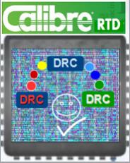
Like the Berkeley’s SPICE and its derivatives in circuit simulation domain, Calibre has been the de facto physical verification tool for over a decade. Now Mentor, a Siemens business, launches a new Calibre based solution dubbed Calibre® RealTime Digital (RTD) – a new physical verification tool that works in concert with popular commercial place-and-route environments.
As design teams use place-and-route to fix violations discovered after full DRC runs, they can use the Calibre RTD tool to make minor changes, thereby resolving DRC violations without causing additional violations — ergo “Correct by Calibre”. Calibre RTD achieves this by making the minor changes and performing customized, smaller and more localized DRC runs to help ensure the violations are removed.
As illustrated in figure 1b, shorter iterations during debug reduce the total number of full-chip pass iterations, allowing designers to dramatically shorten design cycles and get to market sooner. “Calibre RealTime Digital is a solution that was driven by customer requests,” said Joe Sawicki, vice president and general manager of Mentor’s Design-to-Silicon Division.
This roll-out is complementing its earlier 2011 release of Calibre RealTime Custom tool for custom IC design flows. RTD targets the full-chip and block-level digital designs and provides teams designing primarily ASICs and SoCs for various electronics end markets. According to Mentor’s early customers feedback, RTD significantly cut the amount of time needed to reach a DRC clean block. Time saving is ranging from 40% for a design block and up to 85% for ECO’ed block.
“The tool can save time and headaches for design teams developing system chips using any digital process. By working in tandem with the place-and-route tool, Calibre RealTime Digital helps correct physical violation errors that cannot be corrected using a place-and-route system alone. As a result, customers have the potential to get designs to market weeks faster,” Joe added.
Endorsements were already given by several named customers such as Qualcomm and Inphi. “Calibre RealTime Digital is an accelerator to our existing physical verification strategies that fits seamlessly into our design flows, We expect the tool will allow us to cut weeks off of our signoff schedule.” said Weikai Sun, associate vice president of Engineering at Inphi.
RTD and P&R
Enabling RTD physical verification in the RTL-to-GDS2 flow include the following usage scenarios. As illustrated in figure 2a, with RTD designers could do DRC early-on at floorplanning stage, during which an optimal IP or macro placement exploration is being exercised and data flow being analyzed. Furthermore, this also provides a more concrete assessment of area versus performance trade-offs for an IP block during process retargeting. Metal stack selection and routability study are commonly made during this stage in which a balance of route resources for both signal route versus global signals (power, ground and clock networks) is targeted.
Another challenge faced during P&R stage is in dealing with preemptive placements (such as clock headers, special cells) and routings of critical nets (pre-routes) which often times performed by means of augmented internal script-based tool into the formal flow. These preemptive placements or routes may not satisfy all the DRC complex requirements (for example with respect to metal vs via allocation, cut-metal, etc.). Calibre RTD interface lets designers interactively verify DRC, multi-patterning, and pattern matching fixes in P&R using the same sign-off Calibre decks. Hence, these pre-routes or pre-placements could be ascertained as DRC clean prior to setting any dont-touch attribute on the entities.
RTD Usage Models
With Calibre RTD, physical designers are no longer in need of RVE or RealTime-RVE to interface with Calibre verification. Instead, physical verification can be done in physical implementation environment of choice. Some designers who had used Mentor’s Olympus-SoC might be familiar with earlier Calibre InRoute integration.
This time the level of integration is made across major P&R tools.
For custom or mixed signal IPs development, the interaction with either Cadence Virtuoso or Synopsys Custom Compiler is supported as shown in figure 3a. On other hand, for ASIC/SOC physical designers integration with Cadence Innovus and Synopsys ICC2 is available as shown in figure 3b.
With the Calibre RTD release, Mentor has upped the ante in tackling design cycle reduction by doing a shift-left and integrating Calibre physical verification to be part of design implementation. Mentor has reported no meaningful memory footprint impact as RTD should be able to be run on any design size being routable by designers P&R of choice.
Several customer DAC 2018 presentations are scheduled at Mentor’s booth #2621. For more detailed info on Calibre RTD, please check HERE.
What to Expect from Methodics at DAC
I’ve been visiting DAC for decades now, at first as an EDA vendor and since 2004 as a freelance EDA consultant. There’s always a buzz about what’s new, semiconductor industry trends, who is getting acquired and the latest commercial EDA and IP offerings. There’s so much vying for my attention at DAC each year that it can seem like a blur, however I can give you some clarity about a company called Methodics by asking Simon Butler the CEO some questions:
What is Methodics all about?
At this year’s DAC, we’ll be showing a range of solutions for helping manage your IP portfolio, including the latest version of our Percipient IP Lifecycle Management (IPLM) platform. Percipient has evolved to be a real game changer for enterprise-wide coordination of your most critical design assets and a proven way to implement an IP-centric design methodology.
Many vendors talk about PLM, so what’s different with yours?
We’ll also be showcasing how we put the ‘I’ in PLM – our integration with enterprise-class PLM solutions from partners like Siemens that also include world-class version control systems such as Perforce Helix. Please be sure to stop by our booth to say “hello” to our Perforce and Siemens partners who will be joining us to showcase the latest Methodics integrations.
What industry trends do you see this year?
Another big focus for us has been the automotive industry, and the ISO 26262 functional safety requirement specifically. Traceability of designs is an important part of complying with the ISO standard and we’ve got you covered. You can read more about this in our latest white paper, and we have a demo dedicated to this topic at DAC.
We picked up even more automotive know-how at the recent ISO 26262 for Semiconductors conference in Detroit. A lot of the movers and shakers in the car business and their electronics suppliers were at this event. We had chance to offer our thoughts on how IP management is an important consideration, sitting along side ARM, NXP and Intel on a panel discussion.
How do your users share their best practices?
We held our annual Methodics User Group Meeting this month. Our friends at Maxim Integrated were kind enough to host our impressive gathering of customers and lots of great information was shared. Special thanks to Intel, Silicon Labs, Analog Devices, and Maxim for delivering really insightful presentations. The interaction among our users and our own engineering team was fantastic and extremely helpful as we evolve our IPLM solution.
Who is new at Methodics this year?
Vadim Iofis has joined us as VP of Engineering. Vadim brings great insights for implementing solutions on an enterprise level and we’re looking forward to him helping us move further up the value chain of managing our customers most important design assets.
What else will Methodics be doing at DAC this year?
- DAC presentation 62.3 on Wednesday, June 27 in Room 2008 from 3:30 – 5:00pm: “Putting the I in PLM – IPLM Enables a Connected Requirements-driven SoC Methodology”
- Visit us daily for a schedule of interviews to be conducted in our booth by industry luminary Jim Hogan
- Hear the Methodics Jazz ensemble at the Welcome Reception and Hot 55 DAC Kick-off party and at the Monday and Tuesday Networking receptions in the Level 2 lobby from 6 – 7pm
- DAC Give-aways – Register at our booth for a daily drawing for an Echo Spot!
- IP/SOC Program participants – Bring your DAC IP/SOC Passport to our booth to be stamped
ANSYS at DAC
I’m not going to be at DAC this year because I scheduled a fishing trip at the end of June, assuming the show would stay true to form as an early/mid-June event. Still, having to endure salmon and halibut fishing in Alaska rather than slogging around Moscone Center, I can’t pretend to be too disappointed; I’ll be thinking of you all 😎.
One of the things I’ll miss is the ANSYS update on status which, from the information I have, is shaping up to be quite impressive. DAC has accepted 25 ANSYS-related customer papers/posters from all major geographies. Among these the majority seem to come from the who’s who of mobile, while the majority of topics are RedHawk-SC (the big-data version), RedHawk for 3DIC/InFO/CPM and PathFinder (ESD analysis). Good to see these technologies, about which I have been writing for a while, are both trending and translating into successes. (I confess I haven’t seen the papers but I’m assuming no-one wants to brag about failures.)
Vic Kulkarni (VP and Chief Strategist in ANSYS SCBU) gave me a rundown on their theme and events for DAC. The headline is “Beyond Signoff”, getting past traditional margin-constrained analyses to more effective approaches. I wrote about this earlier (breaking out of the box) on my John Lee interview. They’ll be highlighting applications in four main areas:
- Mobile – a lot of innovation still, even though the smartphone market is flattening out (think 5G, basestations, AI, 3D-sensing, …). A lot of activity in advanced packaging.
- High-performance computing (HPC) – CPUs and GPUs of course but also networking and crypto-currency (I learned the in-term for this is now simply crypto. I guess the encryption folks lost that tag.). Advanced packaging big here too.
- 5G/AI – an odd pairing from a solution point of view but it seems both are pushing ultra-high performance, power and reliability hard. Advanced packaging is also big here.
- And of course, automotive – where pretty much everything is critically important, use of advanced processes is becoming more common and there are some moves into advanced packaging, if not quite as aggressive (yet) as in other domains.
The ANSYS story across all these domains remains very consistent – the margin-based approach to design and signoff is breaking down, a point on which I have written multiple times. You don’t have to be a semiconductor expert to understand this. In any type of engineering, the standard way to study the characteristics of a design is vary one thing at a time and hold everything else constant, because we haven’t known how to analyze with everything varying at the same time. We make allowance for variability in other factors through margins – limits on how much each factor can vary, and we repeat analysis at combinations of those extreme cases (the corners).
This approach works fine in many cases, but obviously it is a simplification of a more complex problem. It’s not hard to imagine circumstances under which that simplification would break down, particularly where there may be strong coupling between different factors. In mechanical engineering this happened quite a while ago. Aircraft-engine design requires co-analysis of mechanical, heat and airflow at the same time because analyzing these independently is already known to be dangerously inaccurate. FYI, this co-analysis across multiple domains is commonly known as multi-physics analysis.
Semiconductor design is no different. The question is not if but when co-analysis becomes important in this domain. Perhaps we are so far away from those kinds of interdependency that we can comfortably continue to use our margin-based approaches? Customers using advanced processes and packaging appear to disagree. They’re saying they have to look at multiple factors at the same time, and if they don’t they lose pricing advantage, PPA, yield and even reliability. But I admit I get my information though ANSYS and I’m a sucker for reasonable physics explanations, so you should probably sit in on some of the customer papers at DAC to form your own opinion.
You’ll have multiple chances at DAC to pick apart the story. ANSYS have four customer workshops: design for optimal PPA, early power analysis for IP and chips, accelerating SoC power signoff and multi-physics reliability signoff. They have seven best practices sessions, John Lee (GM) is speaking at a Synopsys special interest group dinner, Norman Chang (CTO) is speaking at an AI/ML workshop and there will be customer presentations at the booth. You can learn more and signup for events HERE. I’ll tell you what I caught when I get back and you can tell me what you thought of the ANSYS story.
HOT Party for a Cause at DAC 55
The Design Automation Conference (DAC), now in its 55[SUP]th[/SUP] year, always offers a lively mix of activities. For EDA vendors and their customers, the focus is on the exhibit floor and in booth suites where the latest technology is on display. For R&D engineers and academics, the technical sessions dig deeply into an increasingly wide range of topics. For every attendee, DAC offers plenty of time for networking and catching up with colleagues from all around the world.
This year’s show in San Francisco offers a unique opportunity for everyone to meet, party, and support a great cause at the same time. The traditional Sunday evening DAC kick-off reception has been combined with the “HOT” party to benefit Heart of Technology and the Gary Smith Memorial Scholarship Endowment at San Jose State University. That one sentence contains multiple hints why this will be one of the hottest EDA events this year; here are some details.
For a start, Sunday evening receptions have been kicking off DAC for many years. Industry luminaries offer their thoughts on the past year and predictions for the next, all accompanied by generous food and beverage service. Do you know what the “DAC glance” is? That’s when you greet a friend or colleague at the reception and immediately look down at his or her badge to check current employment status. Changes from the previous year are not uncommon in EDA.
Over the last few years, a new DAC tradition began with the parties hosted by Heart of Technology (HOT), a philanthropic organization founded by Silicon Valley venture capitalist Jim Hogan. Based in San Jose, HOT rallies the high-tech industry to aid charities throughout the Bay Area in their fundraising efforts. To date, the organization has netted approximately $185,000 to benefit local charities in need.
Last year’s HOT party at DAC in Austin was a benefit for the Gary Smith Memorial Scholarship Endowment and this year we will again support this very worthy cause. Gary Smith was one of the luminaries of EDA, the industry’s most followed analyst, and one heck of a nice guy. He defined market segments, tracked market share, offered revenue projections, published detailed research reports, and served as a tireless advocate for EDA.
There is no better way to celebrate Gary’s extraordinary life than to support the endowment, which offers an award to one undergraduate student annually participating in the San Jose State University Educational Opportunity Program’s Guardian Scholars Program. This program serves youth emancipated from foster care, Wards of the Court, and certified homeless individuals who are highly self-motivated to complete their college education at SJSU.
So now you know the backstory and can appreciate why this combined event at DAC is so significant. The evening starts at 6:00 p.m. on Sunday, June 24th, with the DAC Welcome Reception, including the presentation “EDA Industry Observations and Outlook” from Richard F. Valera, Managing Director, Equity Research at Needham & Company at 7:00 p.m. This is followed immediately by the “HOT 55” party, which will run until 10:30 p.m.
All this happens at Moscone West in San Francisco on the Third Floor Mezzanine. Back by popular demand, Vista Roads Band will provide the entertainment with special guests Methodics Ensemble. There is no ticket or pre-registration required. All DAC attendees and sponsored guests are welcome to the party at no charge, though HOT and the 18 co-sponsoring companies and organizations ask that you donate what you can to the Gary Smith Memorial Scholarship Endowment.
We are certainly looking forward to attending and hope that you can be there as well!
The Wolper Method
If you read around topics in advanced formal verification you’re likely to run into something called Wolper coloring, or what Vigyan Singhal (Chief Oski at Oski) calls the Wolper method. Many domains have specialized techniques but what’s surprising in this instance is a seeming absence of helpful on-line explanations (though there are plenty of resources which cite and use the method without explanation, as if we should already know what it is.) The original source is a paper by Pierre Wolper which may be a little heavy going for some (me too), so I asked Vigyan for help, which he happily provided, adding also some interesting background. What follows is my attempt to provide an explanation for those of us who aren’t CS theoreticians.
Let’s start with the problem the method aims to address. When you want to verify the correctness of data transport logic (in network switches or on-chip interconnects or memory subsystems, for example), checking the protocol is one part of the job, with well-understood dynamic and formal approaches to verification. Checking integrity of the payloads flowing through the network – can they be corrupted in some way – is a different task. At first glance, this could be extremely difficult. In simulation you can’t practically check all possible data values in potentially long sequences and yet it may be far from obvious what corner cases would provide good coverage. And formal methods, even using clever techniques, normally have problems with very long sequences.
Wolper’s contribution was to discover and prove that, as long as control behavior in the logic is independent of payload data, it isn’t necessary to test all possible payload values or long sequences. In fact it is sufficient in formal proofs to use one or two bits in a (payload data) sequence, from which you can provably infer behavior for sequences of arbitrary length. I’m not going to attempt a proof of this; you can read the paper or take it on trust. Instead I’ll give a little background on how this technique found its way into formal verification for hardware, along with a couple of examples of application.
Vigyan told me that when he was working on his doctorate at UC Berkeley, Prof. Bob Brayton directed his formal group to study each week certain papers he would recommend, looking for possible applications in formal methods. Based on the Wolper paper they developed a formal proof approach to checking properties related to a sequence of items transported through a design, in which the design is making decisions about routing, merging and other transport-related activities. So that’s where it all started in our world.
Quite generally they found that using this Wolper technique they could formally detect any possibility that a design could drop, duplicate, corrupt or reorder data, for any possible data sequences. Again, the naive formal approach would check all possibilities out to some sequential depth and then run out of gas. But thanks to Wolper’s insight, they could prove correct behavior using a few specific sequences composed of just a few bits of data, and from that infer correct behavior over arbitrary length sequences.
Using this technique in the simplest case, you would look at only a stream of single bits coming into the router. You constrain to have just two consecutive bits in the stream set to 1 and all others are constrained to zero; importantly, the position of these consecutive bits in the stream should be unconstrained. It’s easy to get tripped up here by a simulation mindset (I did at first). Don’t think of how to set up specific sequences. Think instead of what will be constrained in the proof – two consecutive bits somewhere (unconstrained) set to 1 and all others set to zero. The formal engine will take care of looking for any possible counter-example to this being undisturbed at the output.
These kinds of constraints are what is often referred to as Wolper coloring. You can add an assertion to check transmission at the output of the design using a small state machine. This state machine will accept any sequence of zeros, followed by two consecutive 1’s, followed by any sequence of zeros. But it will error on a single 1 (a bit dropped) or a 101 sequence (maybe an erroneous data insertion or reordering). If the assertion triggers, you have a bug in the transport logic. And if you don’t get an assertion trigger you know, thanks to Wolper, that the transport logic is bug-free for any sequences.
You can continue to refine this to handle more complex transport – if bytes are merged into words on the output, you have to adjust for two streams flowing into one stream. If the design is required to repeat if no response after some time, the check has to allow for that possibility, And so on.
Which makes it rather challenging to produce a canned application (app) to do Wolper checking. Each variant to handle product differentiation, merging options, better error handling, more complex routing, etc, requires modifications to the proof. Perhaps best to think of this as a powerful technique for validating transport correctness, to be used by the full property-checking experts. Where, naturally, Oski would be happy to advise 😎
BTW I have also seen this method referred to as a data-abstraction technique. You are probably familiar with data abstractions when handling memories (reducing a large memory to a single word, byte or bit to simplify a proof). Think of the Wolper method as a way to do a similar thing with data streams – reducing an arbitrary-length stream to just a few bits in the stream.
TSMC OIP DAC Theater Schedule 2018
The TSMC OIP DAC Theater schedule is finalized and ready to go. It kicks off Monday at 10:15 am in booth #1629 and ends with a raffle at 5:45 pm each day (Mon-Tue-Wed) TSMC gives out some very nice prizes so check in with the TSMC booth staff when you arrive. There are 66 coveted presentation spots representing the top ecosystem partners around the world. The TSMC theater is one of the busiest and if you look at the attached schedule you will see why.
TSMC OIP DAC:Overview Schedule Raffle
Honorable mentions go to the presentations by companies that we work with:
- Analog Bits: A Case Study of FinFet SERDES for AI
- ANSYS: ADAS Reliability for Advanced FinFET Design
- Cadence: Virtuoso Design Platform for Advanced Nodes
- Cadence: Advanced Semiconductor Packaging
- Cadence: IP Solutions for Advanced Nodes
- Cadence: High Performance 7nm Digital Design
- Flex Logix: Applications and Value Proposition of eFPGA by Market
- Moortec: FinFET Optimization and Reliability Enhancement
- Mentor: Verification Solutions for TSMC Advanced Packaging
- Mentor: Verification and Advanced DRC
- Mentor: Tessenet DFT Yield Solutions for Advanced Nodes
- SiFive: Enabling Access to Silicon
- Silicon Creations: High Performance PLL Design on 5nm FinFET
- Silvaco: Technology Behind the Chip
- Synopsys: Silicon Proven Designware IP for TSMC Processes
- Synopsys: Power ECOs with ANSYS Redhawk
- Synopsys: Custom Platform for TSMC
- TSMC OIP Update
Special mention goes to Open Silicon who sent abstracts for their TSMC theater presentations:
Topic: Turnkey 2.5D HBM2 ASIC SiP Solution for Deep Learning and Networking Applications
Presenter: Asim Salim / VP of Manufacturing Operations, Open-Silicon
The most common memory requirements for emerging deep learning and networking applications are high bandwidth and density, based on real-time random operations. High Bandwidth Memory (HBM2) meets these requirements and delivers unprecedented bandwidth, power efficiency and small form factor. Open-Silicon’s silicon proven HBM2 IP subsystem in TSMC’s FinFET and CoWoS® technologies is enabling next generation high bandwidth applications and the successful ramping of 2.5D HBM2 ASIC SiP designs into volume production.
Topic:IP Subsystem solutions for Deep Learning and Networking Applications
Presenter: Kalpesh Sanghvi / Technical Manager of IP and Platforms, Open-Silicon
For Deep Learning and Networking applications ASICs, HBM IP Subsystem, Networking IP Subsystem are main building blocks. Open-Silicon’s first HBM2 IP subsystem in 16FF+ is silicon-proven at 2Gbps data rate, achieving bandwidths up to 256GBps. Open-Silicon’s next generation HBM2 IP subsystem supports 2.4Gbps in 16FFC, achieving bandwidths up to >300GBps and supports 3.2Gbps and beyond data rates in 7nm, achieving bandwidths up to >400GBps. Open-Silicon’s Networking IP subsystem includes high-speed chip-to-chip interface Interlaken IP, Ethernet Physical Coding Sublayer (PCS) IP, FlexE IP compliant to OIF Flex Ethernet standard v1.0 and v2.0, and Multi-Channel Multi-Rate Forward Error Correction (MCMR FEC) IP.
Topic:Package Design, Assembly and Test Strategies for Robust 2.5D HBM2 ASIC SiP Manufacturing
Presenter: Abu Eghan / Sr. Manager of Packaging & Assembly, Operations, Open-Silicon
2.5D HBM2 ASIC SiPs manufacturing has unique challenges for package design, assembly and testing both at the wafer level and the SiP level. Open-Silicon’s has proven solutions and strategies that are available to mitigate these issues in order to successfully ramp ASIC SiP designs into volume production.
About DAC
The Design Automation Conference (DAC) is recognized as the premier event for the design of electronic circuits and systems, and for electronic design automation (EDA) and silicon solutions. A diverse worldwide community representing more than 1,000 organizations attends each year, represented by system designers and architects, logic and circuit designers, validation engineers, CAD managers, senior managers and executives to researchers and academicians from leading universities. Close to 60 technical sessions selected by a committee of electronic design experts offer information on recent developments and trends, management practices and new products, methodologies and technologies. A highlight of DAC is its exhibition and suite area with approximately 200 of the leading and emerging EDA, silicon, intellectual property (IP) and design services providers. The conference is sponsored by the Association for Computing Machinery’s Special Interest Group on Design Automation (ACM SIGDA), the Electronic Systems Design Alliance (ESDA), and the Institute of Electrical and Electronics Engineer’s Council on Electronic Design Automation (IEEE CEDA).
Billion Transistor Designs Need Faster Full Chip Tools
During the design cycle as tape out approaches, time pressure usually goes up dramatically. To make matters worse the design itself is much larger, because all the block level work is done and there is a requirement to work with the entire database. It feels like it’s time to put aside the garden trowel and start using a steam shovel. This is when whole-chip DRCs are run and each change needs to be double checked to ensure that no inadvertent changes to the design have been introduced. At this stage, all the tools that were used to initially make the design are most likely sagging under the weight of the fully assembled and nearly finished database. Fortunately, there is an EDA vendor working specifically on solving these design challenges. The Taiwanese company AnaGlobe was founded in 2000 and has a solution for viewing, fixing and comparing the largest design files in existence.
I caught up recently with Ted Chou, AnaGlobe’s Corporate Applications Engineer, to go over their Thunder Integration Platform and Thunder LVL tool. One of their most significant advantages is high capacity and extremely fast database read in and writing. They have their own database called Thunder DB, but can read GDS, LEF/DEF and OASIS. The Thunder DB is about one tenth the size of GDS. Their extremely fast read-in can read in a 17 GB database in around 8.5 minutes. Ted pointed out that other tools can take around 112 minutes for this size design. So, the time saved is significant. Similar gains are seen for database writing. He also pointed out that their performance scales well when additional processors are used.
Their tools operate with the full design in memory, so no viewing or editing operations require disk file access. This makes Thunder a great choice for viewing and fixing DRC errors found with Calibre. AnaGlobe offers an integration with Calibre and ICV. But what appears to be one the most compelling motivation for using Thunder is its LVL capability. Unlike Calibre, no rule deck is needed for Thunder LVL. Another incentive is that you can use your Calibre license for something else when running Thunder LVL, and Thunder only needs one license to run on multiple CPUs, unlike Calibre.
Thunder LVL can run flat or hierarchical. Some of the runtimes that Ted shared with me were impressive. On a 170 GB design file with 393 layers, other tools took 15 hours with 12 CPUs. Thunder LVL ran in 1.7 hours. Thunder LVL also features synchronized viewports for viewing differences in the design that it reports.
There is a lot to say for companies that pick a niche and focus relentlessly on delivering a support product. It helps that the founders come from TSMC and Springsoft, both companies with excellent bona fides. From the looks of it AnaGlobe is enjoying good adoption rates at a number of the largest semiconductor companies. This makes sense because their market focus is on the largest designs. For more information on AnaGlobe and their Thunder products be sure to look at their website.
In an interesting side note, I worked at Calma, the company that created Stream format. In fact, that was the name of their layout editor, GDS II. Yes, there was a GDS I before GDS II, but Stream format was a GDS II utility and was never used with GDS I. I had the opportunity to meet Sheila Brady, the woman that actually wrote the very first Stream import and export utilities. Just to give a frame of reference, this was back the in early 1980’s. It’s testament to some good software design that GDS Stream is still in use today. Of course, it has been adapted to handle today’s more complicated technologies with the addition of more layers and datatypes, and larger record sizes. However, even back then I remember her saying that she really only intended it just to be a tape archive format, not a database for design hand-off, etc.
In one sense, it’s amazing it is still in common use. But this also makes the case for using newer more efficient databases and formats for today’s design challenges. Imagine if you were still using any other technology from 1980 for your daily tasks: floppy disks, 100MHz processors, magnetic tape drives, dial up modems…..

