webinar banner AI 2026 v2

TI: Semiconductor Industry History of Innovation

TI: Semiconductor Industry History of Innovation
by Daniel Nenni on 07-06-2018 at 7:00 am

This is the fifth in the series of “20 Questions with Wally Rhines”

Texas Instruments is a remarkable company founded by remarkable people. And Eric Jonsson was one of the most remarkable visionaries of the 20[SUP]th[/SUP] century. He was a renaissance man who created an industry and a fortune by following the needs of the emerging oil exploration industry, then semiconductors and followed up as a statesman, Mayor of Dallas, to take a city from the depression of being the site of the Kennedy assassination to being one of the most innovative centers of commerce in the 21[SUP]st[/SUP] century. Today, Dallas is home to more than 10,000 corporate headquarters including over twenty Fortune 500 companies. But it didn’t happen by accident.

The roots of TI go back to New Jersey in 1939. J. C. “Doc” Karcher developed reflection seisography technology that could be used to reveal the character of strata beneath the earth and to predict the most likely places to drill for oil. The East Texas oil field moved the center of momentum for the oil exploration industry to Texas and so, Geophysical Services moved with it. Eugene McDermott, Cecil Green, Bates Peacock and Eric Jonsson were the founders. Their technology for seismic analysis became a success and they circumvented the costly approach to becoming a public corporation by acquiring a public company and changing the name to Texas Instruments. The original incorporation was ill timed on December 6, 1941, since the attack on Pearl Harbor the next day changed the whole dynamic of business in the United States.

But these were very adaptable people. They had developed electronic analysis equipment based upon vacuum tubes to use for seismic exploration. Interestingly, the U.S. had no shortage of oil during World War II. What the U.S. needed was electronic equipment for the military. Texas Instruments altered its strategy, developed equipment under contract to the Department of Defense and survived the 1940’s. A Navy procurement Lieutenant, Pat Haggerty, was so impressed with this group from Dallas that he accepted a job with them after the war and eventually became the President and CEO of the company. Haggerty was intrigued by the Bell Labs announcement of the development of the transistor in 1947 and decided that the portable military equipment that TI had developed would benefit from the low power and potentially low cost of transistors. As a result, TI became one the early group of companies that paid the $50K required for a license to produce the germanium transistor that had been developed at Bell Labs.

Not trusting to luck, TI also hired Gordon Teal who had been a primary developer of the techniques to purify germanium to make the transistor possible. Surprisingly, TI emerged as a key contender in the race to produce transistors for military and commercial use. Haggerty was convinced that consumer applications would drive the high volume so, while TI’s initial transistor revenue came from the government, he arranged a deal with Regency, a consumer products company, to market a transistor radio. TI developed the radio and Regency made the money. From then on, Haggerty became convinced that the money for the semiconductor revolution lay within its application to end equipment, a conclusion that drove TI’s strategy to both good, and not so good, results.

How can anyone criticize the evolution of a multi-billion dollar behemoth based upon a Haggerty driven decision to license the Bell Labs transistor? I can’t. It was truly a brilliant move. But the subsequent implementation led to difficulties that might have been avoided.

The drive to develop a silicon transistor was seminal. TI did so through development of the equipment to pull crystals and by understanding the chemistry of germanium, silicon, the dopants and the packaging materials. Two years ahead of the rest of the industry, TI was able to produce silicon transistors whose temperature stability overcame many of the problems of germanium. And the company grew from $20M in annual revenue to $200M in a short period of time.

During the summer of 1958, Jack Kilby, who was a new employee and had no vacation, spent the time of the summer shutdown creating a phase shift oscillator on a single chip with transistors connected with gold wires bonding the discrete devices together on the same chip. Today it seems obvious that multiple transistors on a single chip would be valuable but it wasn’t obvious then. Old timers I met at TI told me that it had been obvious that you could put more than one transistor on the same piece of silicon. “But why would you want to do it?” they asked. “ You would never get both of them working at the same time”. Ridiculous today, as billions of transistors work in harmony to solve problems, but it wasn’t obvious then. It was to Jack, however. And the subsequent litigation over the invention of the integrated circuit led to one of the most significant patent lawsuits of history, creating a career for Roger Borovoy. Jack insisted in his testimony that the words “layed down” applied to deposited metal electrical connections. But TI hired a prestigious law firm that thought the patent suit would be a slam dunk for TI. It wasn’t. Roger, who was corporate counsel for Fairchild, prevailed with the view that the planar process was distinctly different from Jack’s approach to connecting the elements of the integrated circuit. Roger moved on to Intel and became well recognized as a corporate attorney. Jack had to accept the incompetence of the TI-chosen law firm and share the recognition with Robert Noyce (although Noyce’s premature death made Kilby the sole recipient of the Nobel Prize for the integrated circuit). Sharing the recognitions was not a totally negative outcome. While Jack’s words “layed down” may have included the planar process in his view, the compromise to recognize both men settled the West Coast/Dallas dispute and brought us all together, a result that Jack, as a gentle non-argumentative person, would have applauded.

I had the good fortune to meet regularly with Jack. He was a truly wonderful person, very modest and quiet. We both joined the advisory board of Formfactor at Bill Davidow’s request, and I had many delightful discussions with Jack, in addition to those I had early in my TI career.


The 20 Questions with Wally Rhines Series


Liberate Trio Embraces ML and Cloud

Liberate Trio Embraces ML and Cloud
by Alex Tan on 07-05-2018 at 12:00 pm

A chain is as strong as its weakest link. This phrase resonates well in Static Timing Analysis (STA) domain, though it is about accuracy rather than durability. As timing signoff step provides the final performance readings of a design, an STA outcome is as good as its underlying components. Aside from the parasitic extraction accuracy and a delay equation that should be consistent with the upstream place and route tool, design’s cell timing-model accuracy derived from the characterization runs is critical –and could be the weakest link if not handled properly.
Continue reading “Liberate Trio Embraces ML and Cloud”


CEO Interview: Cristian Amitroaie of AMIQ EDA

CEO Interview: Cristian Amitroaie of AMIQ EDA
by Bernard Murphy on 07-05-2018 at 7:00 am

AMIQ EDA has caught my attention over the last few months. My first impression was that this was just another small IDE company trying to compete with established and bundled IDEs from the big 3, a seemingly insurmountable barrier. This view was challenged by an impressive list of testimonials, not just from the little guys but also from designers in many of the bigger companies. In fact, hats off to them also for getting endorsements through this method, bypassing impossible-to-extract corporate endorsements. So it seemed worth learning more about this company. A discussion with Cristian, as the CEO of AMIQ EDA, was a good place to start.

Who is AMIQ EDA?
We’re an EDA company. We provide software tools to help design and verification engineers improve the speed and quality of new code development, simplify legacy code maintenance, accelerate language and methodology learning, and improve source code reliability. Our goal is bolstering the productivity of writing and debugging code while also increasing the chances that the code does what you intend. To use a phrase that I’ve seen before in EDA, we improve engineering efficiency and efficacy. That’s a fancy way of saying that we help design and verification engineers do their jobs.

How did the company start?
AMIQ EDA began in 2008, but we are actually a spinoff from our partner company AMIQ Consulting. They have been providing services and training in functional verification, verification planning and management, verification IP development, and related fields since 2003. In the course of their work they found they lacked certain tools that could make them more effective, so they began developing their own solutions in-house. We formed AMIQ EDA to bring these products to the general market and to develop new tools around similar objectives. This has worked out very well as judged by our customer’s response.

What keeps your customers up at night?
There are many design and verification languages and formats in use today, and it takes time to learn them and to become proficient. There are also numerous libraries and methodologies built on top of these languages, so there is a lot to absorb. We make it easier to learn all this technology, but we don’t stop there. Chip size and complexity continue to grow, and there’s no way that even expert users can manage their design and verification projects with simple text editors and Unix shell utilities. They find especially that it is challenging to keep many different side files (assertions, power intent, testbenches and others) aligned against signal and module names with the RTL as the design evolves.

How does an IDE help them?
For years, software engineers have relied on IDEs to help them write, format, and debug their code. We started development of an IDE for hardware design and verification engineers in 2005, so now we have a mature and full-featured solution: the Design and Verification Tools (DVT) Eclipse Integrated Development Environment (IDE). We support Verilog, SystemVerilog, Verilog AMS, VHDL, VMM, OVM, UVM, UPF, CPF, e, SDL, SLN, and more. We’ve moved into new domains such as power intent verification and portable stimulus specification while continuing to support existing languages and methodologies. DVT Eclipse IDE compiles your code and signals errors as you type, speeds up code writing using auto-complete and quick fix proposals, and finds anything you are looking for instantly. Our customers are very enthusiastic about how much time they save in aligning design and side files through these edit aids, checks and side-by-side views, so much so that they’re already suggesting more ways we can help.

Do you have other products?
Yes, we do. DVT Debugger allows you to perform debugging from the same place where you develop your code. You don’t need to keep switching between your editor and the simulator. DVT Debugger is integrated with all major simulators to bring run-time information into DVT Eclipse IDE. You might wonder why this is needed given the prominence of some commercial debug platforms but in fact a lot of users today work with mixed verification platforms leveraging popular waveform viewers from outside the big 3. DVT Debugger unifies debug in these environments.

If you’re doing verification with SystemVerilog, our Verissimo SystemVerilog Testbench Linter will enforce your specific group or corporate coding guidelines. This ensures consistency and best practices in code development. We build in deep knowledge of the Universal Verification Methodology (UVM) library, but we also support custom SystemVerilog environments. With hundreds of rules inspired by real-life projects, in the past three years Verissimo has been widely adopted as “the testbench linting standard.” Our customers are using Verissimo as part of their everyday code qualification process and they are constantly monitoring code quality using fully automated dashboards.

Finally, Specador is a tool that automatically generates accurate HTML documentation from your source code, even when the code is poorly documented. Most tools that generate documentation just extract and combine comments from your source code. All our tools, including Specador, compile and analyze source code to understand the organization and links within your environment. For example, Specador outputs cross-linked class inheritance trees, design hierarchies, and diagrams. Because the tool is language-aware, the resulting documentation is organized by language specific concepts, including both relationship and structural information.

How big is AMIQ EDA?
We accomplish a lot with a small team of about 15 R&D engineers. We are based in Bucharest, Romania and have sales and support channels around the world. Many people are unfamiliar with the high-tech environment in Romania, where tens of thousands of engineers work for thousands of companies. We have access to a great pool of talent!

Can you identify some of your customers?
Our solutions have been adopted worldwide by more than 100 companies in more than 30 countries. We provide many testimonials directly from our users on our Web site at https://www.dvteclipse.com/testimonials. You’ll see not only that they like our products but also they like our responsiveness. Their needs drive improvements in our products which, as a small company, we can turn around quickly. Proving that you don’t have to be a big company to have popular products!

Where can readers learn more?
Checkout out our website: http://www.amiq.com/

Also Read:

CEO Interview: Jason Oberg of Tortuga Logic

CEO Interview: YJ Su of Anaglobe

CEO Interview: Ramy Iskander of Intento Design


Morris Chang and Me

Morris Chang and Me
by Sunit Rikhi on 07-04-2018 at 12:00 pm

Legend has it that in 1984, Morris Chang was approached by a friend who was looking for money to buy equipment for manufacturing his electronic chip designs. Morris told him to do more homework. When his friend did not return, Morris reached out to him. His friend, it turned out, did not need the money after all. He had found another manufacturer willing to “rent” him equipment capacity at a fraction of the cost.

Morris was intrigued. Moore’s Law was two decades strong, delivering faster, cheaper, and cooler transistors every couple years. More and more chip designers were designing innovative products with these transistors, pushing up the demand for manufacturing. Like his friend, not all chip designers could afford their own manufacturing capacity. Was the world ready for semiconductor manufacturing services?

It took Morris 3 years to answer that question. By 1987, he had launched Taiwan Semiconductor Manufacturing Corporation (TSMC) – a company that manufactured chips for others, as a service. The company is known as a foundry because of the similarity of its business model with that of metal casting foundries in operation since early 19th centur

I never met Morris Chang. But, for the three decades that followed, I was his fellow traveler, a keen observer, a student, and a competitor.

Back in 1984, I was a 27 year old electronics engineer starting my career with Intel. Intel was (and still is) an Integrated Device Manufacturer (IDM). The IDM business model is the opposite of the foundry business model. An IDM develops manufacturing capability for its own products designed by its own IC designers. A foundry on the other hand, develops manufacturing capability for its customers’ products designed by its customers’ IC designers. A foundry helps its customers compete with IDMs.

Intel and TSMC grew up as leaders in the semiconductor industry they helped shape. Both drove exponentials: one in the electronics capability world-wide, and another in the reduction of cost for that capability. It resulted in fundamental changes in the way we live.

For most of this period, the industry generally accepted Intel as the leader at the edge of Moore’s Law, by at least a generation. I was one of the Intel voices shining light on Intel’s lead and explaining how that lead gives a competitive edge to Intel’s chips. Publicly, Morris did not indulge much in the technology leadership question, choosing instead to emphasize TSMC’s brand promise of customer service, trustworthiness and breadth of offerings.

In a 1998 interview, Morris said “The main thing that we’ve learned is that foundry is a service-oriented business, so we are molding ourselves into a service company”. These words were not from a business school slide. They came from deep and powerful insights of a master business man. They captured the pith of TSMC’s winning strategy. An important aspect of the service strategy was the harvesting of immense knowledge from the intimate teamwork between TSMC technologists and its customers’ IC designers. The willingness to learn from his customers was crucial in targeting and tuning his offerings to match his customers’ needs.

His emphasis on customer service did not mean TSMC was not focused on advancing with Moore’s Law. It was. I once described this pursuit as a group led by Intel, running towards an invisible wall, on an increasingly difficult terrain, and in a fog that was getting denser by the year. During this journey, Intel could hear the sounds of rival footsteps behind it, with many growing fainter over time. But not TSMC’s. It had been consistent, even getting louder, as it pulled up to Intel and started running shoulder to shoulder. Morris was clear about the importance of technology in making his customers competitive. In one interview he said “TSMC will stand behind our customers and cooperate with them. The battlefield between our customers and Intel is where we compete against Intel”.

The dawn of this century saw a change in client computing landscape. By then, the computer had spread from the desktop to the lap, but the move to the pocket was just starting. Intel assumed that Intel Architecture would sail into the pocket as easily as it did into the laptop. History however, proved that assumption wrong. The late Paul Otellini, Intel’s CEO at the time, considered that as one of his most significant failures. It was, in fact, Intel’s failure, not just his own. We at Intel felt entitled to success in markets where we were not incumbents. Our actions and inactions were rooted in that. But this was one of TSMC’s most spectacular successes, a result of years of customer-driven learning and delivering to commitments.

By 2008, Intel had launched a foundry division called Intel Custom Foundry (ICF), aiming to manufacture custom products for strategic customers. Intel was not the first to think of creating a foundry within an IDM. IBM offered foundry services long before that, and so did Samsung. However, due to Intel’s reputation as the leader in pursuit of Moore’s Law, even the most skeptical potential customers were intrigued, despite their concerns about incompatibility between the foundry and the IDM models. With ICF, Intel competed directly with TSMC. I led the formation and build up of ICF.

Soon, I came face to face with TSMC on the battlefield. In 2013, Altera Corp decided to switch from TSMC to Intel for their leading edge chips. Although Altera was not one of the highest revenue customers of TSMC, it was a strategic customer because it drove the leading edge of Moore’s Law. At the Q1 2013 TSMC earnings call, Morris was asked questions about the design loss of Altera. He said that he hates to lose even a part of an old customer. He said he regretted the loss and because of this, TSMC had investigated and thoroughly critiqued itself. He continued “..and there were, in fact, many reasons why it happened and we have taken them to heart. It’s a lesson to us and at least, we’ll try our very best not to let similar things happen again”. He clearly held himself accountable for the loss and resolved to do something about it. His humility was admirable and disarming. It kept me from gloating over my win.

Morris Chang was 55 when he started TSMC, and he walked away earlier this month, ending his glorious innings at age 86. This transformational giant of the semiconductor industry taught us through his goal clarity, personal humility, and tenacious stamina, that inspiration can hit at any age, and spectacular climbs to unimagined peaks can be undertaken anytime. Thank you, Morris.


55DAC Trip Report Needham Opening Presentation

55DAC Trip Report Needham Opening Presentation
by Daniel Nenni on 07-04-2018 at 7:00 am

Driving into DAC on Sunday afternoon was a chore since Gay Pride week was finishing with the Gay Pride Parade. Streets were closed, traffic was crazy, and people were roller skating naked which seems wrong on so many levels. This year the opening ceremonies were in the convention center hallway which also seemed wrong. Long lines for food and drink and a small flat screen for the presentation but thankfully no naked roller skaters.

Richard Valera from Needham kicked things off with an EDA overview from the financial side. This is the slot Gary Smith EDA previously occupied. Rich has an EE degree from Carnegie Mellon and spent his first few years in EDA with Racal Redac, Viewlogic, and Synopsys. He then got an MBA/Finance degree from Rutgers and has been at Needham covering technology, including EDA, for the past 20 years. Rich and I are like minds in regards to EDA, absolutely.

Rich went through 20 slides (attached) but it was a bit hard to hear and see so he sent me the slides and we chatted afterwards.

  • What’s driving EDA growth?
  • What’s the growth rate of EDA been doing?
  • EDA IPO’s/Consolidation
  • Private and public investment in the EDA industry
  • Conclusions

Automotive, IoT, AI/ML, and the Cloud are driving EDA of course. We see this on SemiWiki in the categories we track and the domains that visit us. One concern I have, and Rich shares this concern, is that we are experiencing a bubble of design activity especially with Automotive and AI. The last time I talked to Wally Rhines about automotive he compared today’s automotive burst to the one in the early 1900s where there were 285 car companies that narrowed down to 3 and now we are back up to more than 300 car companies suggesting history will repeat itself sooner than later. My bet is much sooner, as in the next 3-5 years.

At a DAC fireside chat Wally reiterated that VC money is back for semiconductor start-ups and the semiconductor industry will continue to grow. More than $900M was invested in 2017 with AI playing a role in the majority if not all of them. Deja vu of the dot com bubble maybe? Successful or not, they all have to buy EDA tools thus the rosy EDA outlook.

Rich discussed the FAANGs (Facebook, Apple, Amazon, Netflix, and Google) which was a new term to me. Amazon, Google, and Facebook are definitely upping their design activity. We see this on SemiWiki. Mostly, in my opinion, it is IP driven traffic with companies doing the “make versus buy” analysis. Our IP readership has always been a strong source of traffic and even more so today. Thus far we have published 761 IP related blogs that have been viewed 3,967,058 times by 26,852 different domains.

Bottom line: Just about everyone on SemiWiki reads about IP, absolutely.

Rich also talked about EDA investment and consolidation. We have a front row seat to this horror show as well. With the Siemens acquisition of Mentor, M&A has heated up a bit. It really is a battle between Synopsys and Mentor with Mentor having the bigger checkbook. SemiWiki has the most complete EDA M&A wiki HERE which was just updated with the Mentor acquisition of Austemper. EDA really is all about M&A and Mentor has the advantage today for the first time in many many years.

Rich then goes into EDA valuations which have risen nicely over the past few years. The reason really is simple and was very clear at the DAC exhibit hall. EDA is now three very dominant companies and a handful of smaller companies caught in between. The SNPS stock price has more than doubled in the past five years and CDNS has more than tripled. The big three EDA companies can now pretty much do whatever they want, they can even skip DAC next year apparently (Synopsys).

Rich’s summary slide:

  • The EDA/Semi IP market is seeing healthy growth, with strength from Auto, IoT, A.I. and relatively new consumers of EDA in the webscale/cloud space.
  • EDA has seen considerable consolidation, which has not been matched by private company formation and IPOs.
  • VC investment has been limited due to smaller TAM size and long gestation of many EDA companies, but opportunities still exist for privates solving challenging problems.
  • Overall (public and private) investment, revenue growth and job growth in the EDA/IP industry remain healthy.
  • And public company investors have shown an increasing appreciation for the value of EDA, as reflected in higher absolute and relative multiples of public EDA companies.

Rich’s presentation is definitely worth a look (attached):

READ MORE 55DAC BLOGS


DAC 2018 Potpourri

DAC 2018 Potpourri
by Alex Tan on 07-03-2018 at 12:00 pm

The venue
Despite of being held at the new three-story Moscone West building, this year 55th DAC in San Francisco bore many similarities as compared with last year’s. Similar booth decors and floorplan positioning of the big two, Synopsys and Cadence, which were across of each other and right next to the first floor entrance –although this time Synopsys had similar screen size for partner presentations as Cadence’s. There were also the same purple-dress magician and the (Penn &) Teller-look-alike comedian at two of the vendor booths; the end-of-each-day poster sessions competing with mouth-watering hors d’oeuvres; and some vendor giveaways luring DAC attendees in hope they also carry along the takeaways from partners’ 10-minute flash presentations. Likewise, many returning vendors and replays of product offerings with incremental updates.

Unique and new things at this year DAC
While from talking with many attendees the sentiment seems to be rather subdued on the exhibit floor, the sheer number of technical papers and behind-closed-door sessions still reflect a leap of enthusiasm in propagating AI, ML and cloud into the EDA space. Key EDA players shared their continued tools benchmarking and rolling out their fruitful collaborative efforts (such as Synopsys Fusion integration with Ansys’ RedHawk, Mentor Calibre-RTD with major P&R tools, Aldecwith its co-simulations, among others).

At this DAC, two seasoned Wall-street EDA/semiconductor analysts (Richard Valera from Needham and Jay Vleeschhouwer from Griffin Securities) were given the opportunity to share their EDA/semiconductor prognosis during Sunday’s DAC kick-off reception and at the Tuesday’s DAC Pavilion session, respectively. They are in agreement that EDA growth is there, although around mid single digit amidst further consolidation of players. Jay also noted that there are more cloud players participation in developing their own silicons (not only doing software developments).

There was Design Infrastructure Alley designated for cloud providers along with Design-on-Cloud pavilion to showcase their EDA on cloud collaborations. Out of the big three, Cadence offers the most comprehensive cloud-enabled solutions including different engagement models while Mentor embraced cloud by offering emulation capabilities on AWS. Despite good traction in addressing cloud technical related aspects such as security and scalability, I believe the cloud adoption is still at the exploration stage. Other than ideally providing capacity at peak demand, the business model portion is still evolving as it is quite a challenge to undo or align major customers existing on-premise capacities with a cloud expansion. On the other hand, it is good news and lowers barrier-of-entry for smaller design houses which may be more ready to embrace metric-based-usage model.

IP is getting more attention
Jay’s feedback on the IP resumption growth resonates well with a number of talks given during DAC. IP has its own ecosystem, encompassing a swath of enablers: from smallest footprint IP providers such as PLL from Silicon Creation to verification IP’s from Synopsys.

In the core IP segment, RISC-V is making a comeback and seems to showcase adopters and aligning a number of talks. Krste Asanovic, Chairman of RISC-V foundation and SiFive co-founder made the Skytalk speech 2 years ago in Austin DAC and it’s Dave Patterson turn this year to make a pitch. “Why open source compilers and operating systems but not ISAs?”, Dave touted. “..The thirst for open architecture that everybody could use and they look all over for the instruction sets and stumbled into ours and liked it and started using it without telling us about it…” Patterson says about his encounters with RISC-V early adopters a few years back. Once realizing of such thirst for an open architecture, it had prompted him and few others to try to make it happen by building the ecosystem through the RISC-V Foundation.

As Synopsys Aart de Geus stated at Silicon Valley SNUGthis year that action is happening at the interface, (Instruction Set Architecture) ISA is the most important interface in a computer system as it connects software to hardware. The motivation behind forming the RISC-V Foundation is also ensuring its openness. According to Rick O’Connor, its executive director, “…so the technology is not controlled by a single company or entity.” He mentioned that using ISA does not require membership or license. Only when it is used as part of non-open-source device or commercial products it requires a RISC-V trademark/license.

While it is a good addition to the core IP selection (as MIPS is now owned by Wave Computing) and Dave showed its anticipated volume ramp, it is still a bit early to make a significant impact on the existing IP-core ecosystem, which is currently being dominated by both X86 and ARM based architectures. Which one will be the leader? Perhaps this involves a bit of reading tea leaves, since it is impossible to predict which one will be dominating IoT and automotive applications.

But ARM has also recently aligned its organization to serve these two-market segments. I asked ARM’s John Ronco, VP & GM of Embedded & Auto Line of Business regarding the appeal of RISC-V instruction set ownership and customization in addressing security related needs, for example. He is not worried as adopters only gain control on the ISA, they still need to design the CPU.

Furthermore, he said “My view on that, vast majority of cases you don’t want to customize the instruction sets. There are two reasons…firstly, actually if you do that you’ll break the software ecosystem. One of the huge benefit of ARM is that you’ve got these vast network of tools/software companies that work on ARM platform…” Secondly, he believes adopters will be confined to incremental customization that offers no performance benefit as they have to ensure no deviations from its fundamental architecture.

ML and AI
At the conference, there were more progress shared by the EDA providers in embedding ML into their solutions. Synopsys shared incremental QoR gains and significant cycle time saving upon deploying ML (and three of their four Fusion interfaces: design, signoff, ECO), while Cadence announced augmenting ML on their characterization tool enabling smart interpolation of points and critical corners to also significantly reduce overall timing library generation. Likewise, Silvaco ML augmentation in behavioral Verilog-A spice modeling generation and its characterization tools has enabled less input collaterals and has reduced the required overall runtime.

As our electronics industry is venturing into the IoT and automotive while sustaining efforts for the upcoming mobile migration towards 5G network, there are many smaller solution providers at the exhibit showing either their niche point-tools or flexible design services. It seems that smaller product form factors, focused functionalities, IP availability and now cloud enablement may have enticed more participants into this foray. Let’s hope it will be more vibrant in Vegas next year!

READ MORE 55DAC BLOGS


Dragonfly-NB2: You Can Have It All in Your IoT Device

Dragonfly-NB2: You Can Have It All in Your IoT Device
by Bernard Murphy on 07-03-2018 at 7:00 am

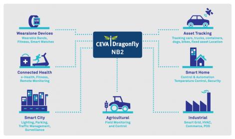
I wrote last month about CEVA’s Dragonfly-NB1 platform, a single-chip IoT solution supporting narrow-band cellular communication; this can meet aggressive total solution price-targets for high-volume deployment, long-range access and the low-power needed for 10+ year battery lifetimes. That solution, based on Release 13 of the standard (also known as NB-IoT or LTE Cat-NB1) saw quick uptake across multiple use-cases. Meantime, opportunities to improve on the standard led to Release 14 (also known as eNB-IoT or LTE Cat-NB2) which now is quickly becoming the mainstream technology for narrow-band. CEVA announced their solution for Release 14 recently at the Shanghai Mobile World Congress.

One feature of Release 14 will sound pretty familiar to low-power experts. Release 13 data rates were pegged relatively low to meet a low-power goal – at peak ~60Kbps – which you would think would be fine for the small data transfers expected in these applications. However, we often see that net low energy is better served by running faster and stopping sooner. This is particularly true for narrow-band cellular where the power amplifier is the biggest power hog. So Release 14 bumps peak rates by as much as a factor of 3; faster transfers and the battery lasts longer!

Another key extension in Release 14 is location support. Here, let’s start with why you would even want location-awareness in an IoT device. For some applications the need is obvious: asset tracking and child-tracking watches (big in China apparently) are examples. But did you know that location-awareness is also valuable in parking meters and street lights, applications not known for mobility? The reason is subtle. While each such device will stay put for its useful life, the system provider and possibly network owners still have to record, at least initially, where the device is; for maintenance, perhaps for billing, for available parking location info and more. You could rely on human input for that data, or you can just take the human out of the loop to get reliable location data across potentially thousands of devices, especially given the small marginal cost to add this feature.

Location-awareness in Release 14 is based on GNSS (pronounced genesis), which is a constellation of positioning standards: the US GPS standard, China’s BeiDou, Russia’s GLONASS and Europe’s Galileo. I had originally wondered about the narrowband positioning reference signal (NPRS) capability in Release 14 as an alternate way to provide location, but according to Emmanuel Gresset (Director Biz Dev in the CEVA Wireless Unit), NPRS locations are quite coarse and are getting only spotty support among operators. NPRS may still provide value in some cases, but GNSS will be a clear leader for most applications.

The Dragonfly-NB2 platform fully supports the Release 14 standard, adding GNSS hardware and software support (as an option) in the modem and the digital front-end. The system supports multi-constellation GNSS with software switching between constellations. CEVA have added instructions to the modem to more efficiently (speed and power) support GNSS so that supporting additional constellations just requires updating the software, which CEVA intends to keep open (the first release, from a 3[SUP]rd[/SUP] party, supports GPS and BeiDou). And naturally it includes interfaces to connect USIM or eSIM for authentication, etc.

Dragonfly-NB2 continues to offer the advantages of NB1, providing all the components you need, including RF transceiver and power amplifier; just add embedded flash and sensors/sensor-interface and you have a single chip solution. You can run application software on the CEVA-X1 platform at competitive MCU performance in addition to supporting communication functions. CEVA have also added deep-sleep capability to further reduce standby power for that 10-year battery life goal. Emmanuel says you can expect to see full silicon-proven reference boards (with RF) to support application software design in Q3, based on both 55nm and 40nm processes.

Since CEVA are already well known for voice-based capabilities, they also offer voice-activation through their ClearVox software as an option. I’ve written about this capability in other blogs – voice activity detection, beam-forming support, noise suppression, always-on voice-trigger, command and sound detection. Imagine a medical alert system activated by voice rather than pushing a button, or a home protection system detecting the sound of broken glass.

This is a pretty impressive package – cellular communication, location aware, voice activation, ultra-low power. Is it overkill? Not according to recent survey information from Ericsson which Emmanuel shared with me (Ericsson Mobility Report 2018). Adoption of Release 13 + Release 14 is expected to grow at 30% CAGR through 2023, and Emmanuel expects Release 14 to quickly dominate this growth for all the reasons outlined earlier.

A lot of this is being driven by new systems entrepreneurs, like smart bike and scooter providers, parking space trackers, recycling systems and other rapidly-emerging solutions. Each is looking for differentiation in capability, through power, location-awareness, even voice-activation. And they’re also looking for differentiation in cost, where more are now going around the standard supply chain, wanting to squeeze price through single-chip solutions by working directly with IP and ASIC vendors.

So I’m guessing this probably isn’t overkill. Across the boundless range of possible IoT innovation, ability to pick and choose the capabilities you want, especially with hot features like voice activation (no need for panels or buttons), this looks like a great platform on which to build. You can learn more about Dragonfly-NB2 HERE.


IITC – Imec Presents Copper, Cobalt and Ruthenium Interconnect Results

IITC – Imec Presents Copper, Cobalt and Ruthenium Interconnect Results
by Scotten Jones on 07-02-2018 at 12:00 pm

The IEEE Interconnect Technology Conference (IITC): Advanced Metallization Conference was held June 4th through 7th in Santa Clara. Imec presented multiple papers on comparing copper, cobalt and ruthenium interconnect. One paper in particular caught my eye: Marleen H. van der Veen, # N. Heylen, O. Varela Pedreira, S. Decoster, V. Vega Gonzalez, N. Jourdan, H. Struyf, K. Croes, C. J. Wilson, and Zs. Tőkei, “Damascene benchmark of Ru, Co and Cu in scaled dimensions” and I had the chance to not only review the paper but also to interview one of the papers authors, Zsolt Tokeis.

Background
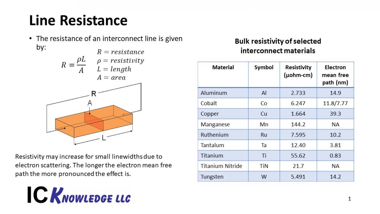
The resistance of an interconnect line depends on the line length, cross sectional area and the resistivity of the material, see figure 1.

Figure 1. Line Resistance and Material Properties.

On the left side of figure 1 is the formula to determine the resistance of an interconnect line. On the right side of the figure is the bulk resistivity and electron mean free path for selected materials. From the table it can be seen that copper has the lowest bulk resistivity of any of the listed materials, however as the cross-sectional area of an interconnect lines scales down resistivity increases due to scattering. The longer the electron mean free path is in a material the more the resistivity increases as the area is reduced. Copper has a long electron mean free path and is strongly affected by cross sectional area.

The other issue with copper is a barrier layer is required to prevent the copper from contaminating the rest of the structure. Barrier layers are made of materials such as Tantalum Nitride with very high resistivity and the barriers don’t scale down in thickness as the cross sectional area scales down, see figure 2.

Figure 2. Copper Scaling.

Currently copper barriers are around 2nm to 4nm in thickness with 2nm a lower limit. From the figure you can see that scaling from a 14nm node to a 10nm node reduces the copper cross sectional area to 0.33x for a 4nm barrier and 0.48x for a 2nm barrier.

The problems with increasing resistivity as linewidths shrink and barrier resistance open the door for other materials to displace copper at small linewidths if the resistivity doesn’t increase as much with cross sectional area and thinner or no barrier can implementations are possible.

Cobalt and Ruthenium are the two leading materials to replace copper at small dimensions.

Imec Line Resistance Results
Imec created 15nm trench openings on a 44nm pitch and then shrunk the trench width by depositing a conformal SiO[SUB]2[/SUB] layer using Atomic Layer Deposition (ALD). The resistance of lines created by filling the trenches with various were then measured. Figure 3 is the measured resistance of the lines.

Figure 3. Line Resistance Versus Conductor Area
(figure 3 from the imec paper).

Figure 3 from the papers looks at copper with a 2nm barrier (the minimum achievable) versus cobalt and ruthenium with no barriers and 0.3nm adhesion layers. Cobalt and Ruthenium migrate less than copper and can be used without barriers (more on this later).

Plot (a) in the figure is the line resistance versus the cross-sectional area of the conductor material with the cross-sectional area determined electrically and excluding the barrier. From the figure you can see that the resistance goes up for all materials as the cross-sectional area is reduced with copper always having the lowest resistance. Plot (b) in the figure is the resistance of the overall line including barriers and shows that at around 300nm[SUP]2[/SUP] conductor cross-sectional area cobalt and ruthenium are superior to copper.

For a typical aspect ratio this is equivalent to an approximately 12nm linewidth. For advanced nodes there is a trend for critical interconnect layers to have wide lines and narrow spaces between the lines to minimize resistance. A 12nm line would be typical from something like a 16nm pitch, smaller than is likely to be required any time soon.

Via Resistance
For the lower level interconnects lines are relatively short and vias are common. Via resistance can therefore become a very important factor in interconnect resistance and barriers in vias contribute a lot of resistance. Figure 4 illustrates the via resistance versus critical dimension (CD).


Figure 4. Via Resistance Versus CD
(figure 5 in the imec paper).

Figure 4 compares ruthenium with no barrier, cobalt with no barrier, cobalt with a 1nm titanium nitride barrier and copper with a 1nm ruthenium barrier and 1.5nm tantalum nitride barrier. At all CDs ruthenium and cobalt outperform copper. It has been found that barrier-less cobalt is only usable with dense inter level dielectric layers so some barrier may be required depending on the ILD. Ruthenium does not require a barrier at all.

The lower resistance of cobalt and ruthenium vias shifts the pitch at which teh material out perform copper. It is somewhat design dependent but at a 40nm pitch copper is the best, by the time you scale down to 32nm pitch cobalt and ruthenium perform better.

Currently cobalt has been implemented by some companies for contacts at 7nm and Intel is using cobalt interconnect for soem levels for their 10nm (roughly equivalent to foundry 7nm) technology. Ruthenium has the best via and interconnect resistance at small dimension but is very difficult to process.

Electromigration
Even with the relatively small currents that exist in state-of-the art ICs, the small cross-sectional area of the conductors leads to high current density. Momentum transfer from electrons to the conductor atoms can cause the conductor atoms to migrate and eventually create breaks in the conductor. This is referred to as electromigration and is a serious issue particularly in higher performance designs. The electromigration resistance of a material can be characterized by the activation energy of the material for electromigration to occur where the activation energy is an exponential factor. The electromigration activation energy is proportional to the materials melting point and cobalt and particularly ruthenium shows greatly improved electromigration resistance compared to copper.

Discussion

Taking line resistance, via resistance and electromigration into account imec draws the line at around a 40nm pitch for cobalt or ruthenium to outperform copper.

Imec is working on a barrier-less cobalt solution with dense low-k iILD materials, electromigration performance is good but without a barrier cobalt does intermix with copper where the two materials come into contact at high interconnect levels.

Ruthenium doesn’t need a barrier but CMP of ruthenium is still problematic.


55DAC Trip Report with Drama

55DAC Trip Report with Drama
by Daniel Nenni on 07-02-2018 at 7:00 am

This was my 35th DAC and it did not disappoint, especially when it came to the DAC Drama Department. This year DAC proved once again that it is THE place for semiconductor professionals and academics to learn and network. The big news is that Synopsys did not reserve a booth for 56DAC in Las Vegas next year which resulted in quite a bit of drama.

In my opinion the actual location of DAC is not as big of a deal as it seems. The number one critical feature of any conference is content. Without great content it does not matter where it is located and by content I am talking about the actual conference, not what’s happening on the exhibit floor.

The second critical conference feature is promotion. You have to get the word out to the masses. As a mature industry new faces are always important, especially in the academic community as they are our future.

Third of course is location. I have been to DACs all over North America including my first one in Albuquerque NM, two in Las Vegas and two in New Orleans of all places. San Francisco, San Diego, and Anaheim are popular destinations because let’s face it, California is the best location, absolutely. For the life of me I do not know why it has never been in San Jose but that is another story.

Back to the drama of Synopsys not exhibiting at 56DAC. The first question I have is: “Does it really matter?” To me the answer is no, Synopsys not exhibiting will not change my plans at all. My beautiful wife and I are both attending 56DAC, we both enjoy Las Vegas and are really looking forward to it. In fact, my wife’s first DAC was 1985 in Las Vegas. The picture above is from our 30th wedding anniversary in Las Vegas where we renewed our vows. Kind of a spur of the moment thing. We actually went there to see Elton John but I digress…

By the way, this would not be the first time a leading EDA company skipped exhibiting at DAC. Cadence did it a number of years ago when it was in San Francisco. Instead they rented space at the Four Seasons hotel across the street. That was pretty much the end of Cadence CEO Mike Fister. EDA and IP customers will always have a choice and how a company behaves can sway that choice one way or another, believe me.

To be clear, just because Synopsys may not exhibit I can assure you they will still be part of the DAC sessions and panels. The only real difference will be a lot less purple running around and I am okay with that.

Based on what I was told by people that know, 56DAC will in fact be in Las Vegas no matter which vendors decide not to show up. 57DAC however will probably be co-located with SEMICON WEST in San Francisco. I also attend SEMICON and feel co-location would be a 1+1=3 proposition. Semiconductor design and semiconductor manufacturing has never been closer and it will continue to cross even more paths as we introduce new process technologies, my opinion.

This year more than 20,000 people are expected to attend SEMICON WEST as compared to around 6,000 people at DAC:

“From materials, equipment, design, manufacturing, system integration, and demand channels to new verticals and adjacencies such as Flexible Hybrid Electronics, MEMS & Sensors, you’ll gain access to the best in the business and get a glimpse at what’s next. Immersive, new experiences demonstrating hot-buttons like Smart Transportation, Smart Manufacturing, MedTech, Big Data, IoT, and the cognitive technologies that are transforming the world make this year’s Expo like no other before.”

Sounds like a great fit to me!

READ MORE 55DAC BLOGS


Trump is the greatest gift that Twitter could have asked for!

Trump is the greatest gift that Twitter could have asked for!
by Vivek Wadhwa on 07-01-2018 at 7:00 am

In the 1930s, psychologist B.F. Skinner put rats in boxes and taught them to push levers to receive a food pellet. The pushed the levers only when hungry, though. To get the rats to press the lever repeatedly, even when they did not need food, he gave them a pellet only some of the time, a concept now known as intermittent variable rewards. Casinos have used this same technique for decades to keep us pouring money into slot machines. And now the technology industry is using it to keep us checking our smartphones for emails, for new followers on Twitter, or for more “likes” on photographs we posted on Facebook.

It’s also the technique Donald Trump has mastered with his tweets. Whether on the left or the right, we are now so addicted to this erratic stream of controversy that we must, must, must check our social media far more often to witness the latest twist. In other words, we are now a national Skinner Box experiment, a country of rats waiting for the food pellet to fall.

Ironically, the greatest beneficiaries of this growing addiction to the crazy political news cycle are none other than the technology companies that make it possible. Donald Trump is their greatest gift, and they are his. Social media have become the equivalent of rat pellets, and the technologies that were supposed to bring humanity together and satisfy our social cravings are instead tearing societies apart.

This is something that Alex Salkever and I explain in our new book, Your Happiness Was Hacked: Why Tech Is Winning the Battle to Control Your Brain—and How to Fight Back.We are never sure whether someone has retweeted, “liked”, or commented on our posts, so we return to our devices all the time and, in doing so, end up being sucked into the rabbit hole. This induces release of dopamine, a neurotransmitter related to feelings of satisfaction. The resultant feeling of satisfaction is very short term, though, and is often followed by longer-lasting feelings of frustration and regret at having wasted time and allowed another to hijack our brains and our attention.

One motivator dependent upon intermittent variable rewards is the fear of missing out (FOMO). FOMO is a tangible feeling that we are being left out of a conversation or event that is important to our social status, work, or position in society. FOMO commonly happens at work. And now, our president has pushed FOMO aggressively into the social realm. We feel a need to know what’s happening because so much is happening and it’s all so crazy!

The media that we consume as a result of these manipulations tend to be biased toward events that have a very negative effect on us. It may be important that we know what is happening in the world around us, especially if we are to change it. But absorbing too much news of negative events trains us to perceive them to be more likely than they actually are to affect us directly. Talk of the invasion of America by gangs of the transnational criminal organization MS-13 induces people to fear gang activity even in places where MS-13 has no presence. That effect occurs amongst both Trump supporters and Trump opponents, because the part of our mind that processes deep fears still factors in information that our logical minds would declare false.

Of course, the ubiquity of certain negative stories of even marginal makes those stories appear highly relevant to everyday life, leading to greater consumption of the technology platforms that publish them. Until the last elections, Twitter was essentially dying. Yet, following the election, in its 2017 annual report, Twitter stated that, though user numbers had grown by just 4%, engagement had grown by a very substantial 12%. More engagement means more ads and a feedback loop that is stronger and therefore harder to exit or to consciously opt out of.

Twitter is Trump’s platform of choice, of course. But the behaviors that Trump’s use of it encourages in all of us feed into the advertising-revenue streams of all major online search engines and social media. Thus many apps now employ the convention of using a red dot on an icon or on a menu to indicate that an update, message, or other form of communication is awaiting our attention. And the growth of this compulsive behavior conversely robs us of control and poisons our world view.

We don’t want to check Twitter more often. It makes us dissatisfied, even grumpy. And we don’t want to think only about the bad things in life. But we feel powerless to control the information that overwhelms us via our friends and everything else we consume to learn about the world.

So this presidential term is, if nothing else, a gift to the tech companies that benefit from the behaviors that actors in the political realm are constantly reinforcing in the population. And if you have felt your life to be less under your own control since the nation entered this new Skinner Box phase, that may be because it is.

For more, please read my new book,Your Happiness Was Hacked: Why Tech Is Winning the Battle to Control Your Brain—and How to Fight Back.