webinar banner AI 2026 v2

Know what 5G is? You’re probably wrong

Know what 5G is? You’re probably wrong
by Tom Simon on 07-12-2018 at 12:00 pm

If you think the transition to 5G will be anything like the transitions before it to 3G or 4G, you are in for a big surprise. Not only will the transition take longer than either of the previous transitions, its ramifications will spread far beyond cell phones and into other areas such as automobiles, AI, healthcare, and commerce. This is because 5G is not just about higher data rates or carrier efficiency. It will involve multiple bandwidths, a wide range of devices and new modalities of communication. Even though we are approaching its initial implementation, the specification is still in flux and has yet to be finalized. This makes it so that nobody, even the experts, know what 5G really is.

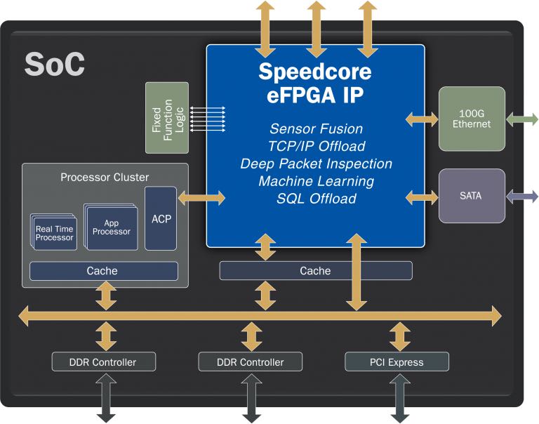
5G is certain to bring big changes in mobile data applications. Many companies are working toward helping to create and enable 5G hardware or to implement solutions that rely on it. One such company is Achronix. Their embedded FPGA fabric – SpeedCore eFPGA – is ideal for dealing with the need to implement 5G systems in the face of changing requirements and specifications. I recently spoke to Mike Fitton, Senior Director of Strategic Planning, at Achronix, who moved there from Intel for exactly this reason. He sees huge opportunities with 5G and understands that Achronix can play a pivotal role.

One of the most interesting areas in 5G is what is called V2X, which is the catch phrase for communications from a vehicle to anything. This includes vehicle to vehicle communication, which can help vehicles negotiate with each other and share alerts about hazards. V2X also includes things like road construction beacons informing cars of reduced speeds or lane diversions. Mike talked about how important URLLC or Ultra Reliable Low Latency Communication will be for these applications. There will be new standards and tightly coupled protocols that will necessarily be evolving. Having the ability to modify algorithms easily without respinning silicon will be extremely helpful. Low latency in communication will also be essential. Mike pointed out that on-chip FPGA fabrics will afford latency on the order of nanoseconds, as opposed to microseconds with off-chip alternatives.

Mike pointed out that everyone was surprised when SMS turned out to be the killer app for communicating with smart phones. It will be just as hard to predict what will be big with the new modes of communication that 5G will bring to the table. Regardless, flexibility will play a big role in developing system based on 5G. Mike and I discussed some examples of how 5G can be utilized. Low power and low bandwidth connections supporting IoT applications can be used to request services automatically over inexpensive and widely available links. For instance, paper shredding bins could automatically message the mother ship to send a mobile shredding truck when they are nearing full. Another example I heard of was where remote fuel tanks for water pumps on farms could signal when they need to be refilled. The savings and increased efficiencies in either of these scenarios are very compelling. This is just a small taste of the new use models that could become practical with the advent of 5G.

The evolution of 5G will be very interesting. At first it will be offered as an assisted mode for LTE, then later we will see a wholesale switch to all the elements of 5G. Necessarily the high frequency, short range component will come later. There are significant technical challenges due to interference and blockages at short wavelengths. Trials for 5G will be starting in 2020. During the initial implementation stages operators and system developers will place a premium on adaptability and the ability to provide quick updates to address unforeseen issues. Achronix is sure to play a role in this market with SpeedCore eFPGA’s combination of low power, high performance and rapid reconfigurability. For more information on how embedded FPGA fabric can facilitate 5G implementation, take a look at the Achronix website.



Deep Learning: Diminishing Returns?

Deep Learning: Diminishing Returns?
by Bernard Murphy on 07-12-2018 at 7:00 am

Deep learning (DL) has become the oracle of our age – the universal technology we turn to for answers to almost any hard problem. This is not surprising; its strength in image and speech recognition, language processing and multiple other domains amaze and shock us, to the point that we’re now debating AI singularities. But then, given a little historical and engineering perspective, we should remember that anything we have ever invented, however useful, has always been incremental and bounded. Only our imagination is unbounded. If it can do some things we can do, why should it not be able to do everything we can do and more?

So it should not come as a surprise that DL also has feet of clay. This is spelled out in a detailed paper from NYU, in 10 carefully elaborated limitations to the method. The author, Gary Marcus, is somewhat uniquely positioned to write this review since he is a professor of psychology and researches both natural and artificial intelligence. Lest you think that means he has only a theoretical understanding of AI, he founded his own machine learning company, later acquired by Uber. I quickly summarize his points below, noting his caveat that all points made are for what we know today. Advances can of course reduce or even eliminate some limits, but the overall impression suggests the big wins in DL may be behind us.

In his view, the CNN approach is simply too data hungry, not just in recognition but also in generalizing, requiring exponentially increasing levels of training data to generalize even at relatively basic levels. DL as currently understood is ultimately a statistical modeling method which can map new data within the bounds of the data it has seen but is unable to map reliably outside that set and especially cannot generalize or abstract.

Despite the name, DL is relatively shallow and brittle. While it seems from game-playing examples with Atari Breakout that DL can achieve amazing results such as learning to dig a tunnel through a wall, further research shows it learned no such thing. Success rates drop dramatically on minor variations to scenarios, such as moving the location of a wall or changing the height of a paddle. DL didn’t infer a general solution, and what it did infer breaks down quickly under minor variations. On a different and funny note, the British police wanted to use AI to detect porn on seized computers; unfortunately it keeps mistaking sand dunes for nudes, rather a problem since screensaver defaults often include pictures of deserts. More troubling, there are now numerous reports on how easily DL can be fooled through individual pixel changes.

DL has no obvious way to handle hierarchy, a significant limitation when it comes to natural language processing or any other function where understanding requires recognition of sub-components and sub-sub-components and how these fit together in a larger context. Understanding hierarchy is also important in abstraction and generalization. DL understanding however is flat. Systems like RNNs have made some improvements but have been shown in research last year to fall apart rather quicly when tested against modest deviations from the training set.

DL can’t handle open-ended inference. In reading comprehension, drawing conclusions by combining inferences from multiple sentences is still a research problem. Inferencing with even basic commonsense understanding (not stated anywhere in the text) is obviously harder still. Yet these are fundamental to broader understanding, at least understanding that we would consider useful. He offers a few examples which would present no problem to us but are far outside the capabilities of DL today: Who is taller, Prince William or his baby son Prince George? Can you make a salad out of a polyester shirt? If you stick a pin into a carrot, does it make a hole in the carrot or in the pin?

DL is not sufficiently transparent – this is a well-known problem. When a DL system identifies something, the reason for a match is buried in thousands or perhaps millions of low-level parameters, from which there is no obvious way to extract a high-level chain of reasoning to explain the chosen match. Which is maybe not a problem when matching dog breeds, but when decision outcomes are critical as in medical diagnoses, not knowing why isn’t good enough especially bearing in mind the earlier-mentioned brittleness of identification. Progress is being made but this is still very much at an early stage and it is still unclear how deterministic this can ultimately be.

Generalizing an earlier point, the DL training approach doesn’t provide a method to incorporate (and apparently in a lot of research even actively avoids) prior knowledge such as the physics of a situation. All work of which the author is aware works on bounded set of data with no external inputs. If we as a species were still doing that we would still be banging rocks together. Our intelligence very much depends on accumulated prior knowledge.

One problem in DL could equally be assigned to humans (and Big Data while we’re at it) – an inability to distinguish between correlation and causation. DL is a statistical fitting mechanism. If variables are correlated, they are correlated and nothing more. This doesn’t mean one caused the other; correlation might result through hidden variables or over-constraints. However understanding what might be a true cause is fundamental to intelligence, at least if we want AI to do better than some of us.

There is no evidence that DL would be able to handle evolving conditions, in fact there is a cautionary counter-example. Google Flu Trends aimed to predict flu trends based on Google searches on flu-related topics. Famously, while it did well for a couple of years, it missed the peak of the 2013 outbreak. Conditions evolve, and viruses evolve. Google Flu Trends didn’t use DL as far as I know, but there’s no obvious reason why a dataset for a problem in this general (evolving) class would not be used for DL training. Self-training (after bootstrapping from a labeled training set) may be able to help here, but it can’t model disruptive changes without also considering external factors of which even we may not be aware.

Prof. Marcus closes his ten points (which I compressed) with an assertion that DL still doesn’t rise to what we would normally consider a reliable engineering discipline, where we construct simple systems with reliable performance guarantees and out of those construct more complex systems for which we can also derive reliable performance guarantees. It’s still arguably more art than science, still not quite out of the lab in terms of robustness, debuggability and replicability and still not easily transferred to broader application and maintenance by anyone other than experts.

None of which is to say that Prof. Marcus disapproves of DL. In his view it is a solid statistical technique to capture information from large data sets to draw approximate inferences for new data within the domain of that data set. Where things go wrong is when we try to over-extend this “intelligence” to larger expectations of intelligence. His biggest fear is that AI investment could become trapped in over-reliance on DL, when other apparently riskier directions should be just as actively pursued. As a physicist I think of string theory, which became just such a trap for fundamental physics for many years. String theory is still vibrant, as DL will continue to be, but happily physics seems to have broken free of the idea that it must be the foundation for everything. Hopefully we’ll learn that lesson rather more quickly in AI.


Cadence’s Smarter and Faster Verification in the Era of Machine Learning, AI, and Big Data Analytics Panel

Cadence’s Smarter and Faster Verification in the Era of Machine Learning, AI, and Big Data Analytics Panel
by Camille Kokozaki on 07-11-2018 at 12:00 pm

I attended on Monday, June 25, DAC’s Opening Day, a Cadence-sponsored Lunch panel. Ann Steffora Mutschler (Semiconductor Engineering) was the Moderator and the Panelists were Jim Hogan (Vista Ventures), David Lacey (HP Enterprise), Shigeo Oshima (Toshiba Memory Corp), Paul Cunningham (Cadence).
Continue reading “Cadence’s Smarter and Faster Verification in the Era of Machine Learning, AI, and Big Data Analytics Panel”


Glad to be part of SemiWiki and my DAC Industry Report

Glad to be part of SemiWiki and my DAC Industry Report
by Mark Gilbert on 07-11-2018 at 7:00 am

Welcome to my newly relocated column, I am so excited about my new relationship with Daniel Nenni, and the other esteemed bloggers on SemiWiki. For those who do not know me, I have been a featured columnist on another EDA portal for the past 12-plus years, and in EDA for 20-plus years. As the leading recruiter in our industry, (or so I am told), I write about our industry from a non-technical viewpoint, as well as talk about the various hiring modalities and industry-specific career advice. For my first column, should I say blog, on SemiWiki, I want to talk about this past DAC and what might be coming down the DAC road, as well as how hiring in general, is going.

First, let me address the brains at DAC; it doesn’t take a PhD to know that DAC should always be held in the Bay area. While the last two DACS in Austin were OK, (and understandably need to be hosted in Austin occasionally, as it is the 2[SUP]nd[/SUP] busiest U.S. hub for EDA/SEMI), they should still be hosted in the Bay area, almost always, even if the dates vary. Vegas makes no sense! I know it is said that many of us love to go to Vegas, but that in and of itself is not enough of a reason to host there. Make no mistake, I personally can go anywhere, but most companies will only send a limited number of people to alternate destinations, if at all. Having DAC where the base lives simply makes the most sense, both economically and practically.

To complicate this, DAC has new owners, which made DAC’s future the talk of the Conference. In general people wondered:

[LIST=1]

  • Will it return, and that answer is unequivocally YES
  • Will it be in VEGAS, and that answer is 98% YES. The venue is reserved well in advance and paid for similarly. I cannot imagine them losing all that money…also, companies all selected their locations while at DAC, and while there were rumors that perhaps DAC will combine with SEMICON, no one knows if that will actually happen for this, or any other DAC. (Though my guess is it is likely).

    DAC 2018 was indeed quite busy, and in fact I thought the first Monday was the busiest I have seen in several years. In talking with so many C-Level executives over the three days I was there (from open to close), most were pretty happy with the show. I have said it before and I will repeat it now: …DAC is not a consumer show and numbers do not tell the whole story. It is WHO is there and if YOU had something that they wanted.

    Those that scheduled in advance, or had inviting booths with the right (enticing) information that compelled people to want to know more and the personnel that knew the right people that could actually get them in for a demo, did well. If demos were not an option then hopefully a future on-site visit was scheduled. That is what makes for a successful DAC…Those that sat in their seats waiting for someone to beg them to show them what they have or that put no effort into their booth, are still sitting in their seats. (Candy seemed to be the #1 option, lots of candy!)

    DAC is different these days…How you ask??? Well, in case you have not heard, which means you do not have internet or are taking too much sleep medication, acquisitions have changed our landscape. Instead of a lot of new EDA start-ups, DAC was littered with IP companies… a LOT of IP companies. A cloud aisle was added this year for various collaboration/version control type offerings, but CLIOSOFT clearly leads the way there, with a few others making significant headway.

    As for hiring, normally I walk away with several new companies and requisitions, but not as much this year. Let me be clear, that is not a statement on hiring; for me, DAC is all about building and maintaining relationships, and learning more about what’s hot, what’s coming, what’s happening, and for using that as a barometer, it was great success for me. I made so many new connections that want to work together, and while those needs will be spread over time, expertise, and locations, most will bear fruit. Hiring remains extremely difficult as the needs are plenty and the pool shallow, with good people not wanting to leave. Companies have needs and it is harder than ever to find good qualified people (which I will talk about more in my upcoming columns).

    I went to two really great parties, the Cliosoft/AUSDIA party and the ONESPIN party, and I must say they were two of my all-time favorite events. I was too tired to go to the Denali/(Cadence) party this year, the first one I’ve missed since its inception, but I am sure not much has changed since it stays pretty much the same every year. My trademarked White sports coat was as always, quite noticed and as my friend Craig Shirley (the new CEO of OSKI) said, “one day that jacket will be retired to the archives of our history” (or something like that, I hope that means I can sell them).

    I look forward to a great relationship with SemiWiki and will have my Blog published here monthly. If I can ever be of help to any of you, my advice is always free and gladly given…

    EDA-Careers is a highly specialized recruiting agency that recruits specifically for everything EDA/Semiconductor and IOT… All Levels, All Specialties. R&D Developers, Application Engineers, Designers, Sales and Marketing WE DO IT ALL!

    EDA-CAREERSis a unique and very different company when it comes to how we handle our clients and candidates. With nearly 20 years of recruiting exclusively in the EDA/Semiconductor industry, we pride ourselves on our relationships and follow-up. We WORK HARD to help find the best candidates for our companies and the best opportunities for our candidates, making sure both are satisfied every step of the way. In effect, we become PARTNERS so that both the candidate and the company process goes smoothly, from beginning to end. That is why we have worked successfully with Hundreds of companies and placed such a broad array of candidates.

    More 55DAC blogs


  • A New Kind of Analog EDA Company

    A New Kind of Analog EDA Company
    by Daniel Payne on 07-10-2018 at 12:00 pm

    My IC design career started out with circuit design of DRAMS, so I got to quickly learn all about transistor-level design at the number one IDM in the world, Intel at the time. In the early days, circa 1978 we circuit designers actually had few EDA tools, mostly a SPICE circuit simulator followed by manual extraction, manual netlisting, manual layout, manual DRC, and of course, manual transistor sizing. In 2018 the scene has changed for the better because EDA companies have offered up lots of point tools to eliminate all of that manual, error-prone work that I had to grok through in the 1970’s.

    I’ve been reading up on a new EDA company focused on automating some of the analog IC design challenges, and wanted to blog about it here to share what’s new and different at Intento Design, a company that I visited at #55DAC last month in SFO. The tagline at Intento Design is, “Responsive EDA for Analog IP”. For web sites I know what responsive design means, but for the phrase responsive EDA I needed to dig a bit deeper. A recent press releasefrom June 7th revealed that STMicroelectronics is using a tool called ID-Xplore on their FDSOI circuits in the Aerospace Defense & Legacy Division for:

    • Design exploration
    • IP reuse
    • Use in a Cadence environment
    • Technology independent constraints

    OK, that sounds great, but how does ID-Xplore actually work?

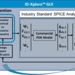
    Here’s a tool flow diagram to explain what goes into and out of IC-Xplore:

    The SPICE analysis portion in the middle immediately caught my eye, yet the company isn’t offering a SPICE circuit simulator, instead they are using SPICE-accurate analysis to help size transistors from a traditional schematic tool like Virtuoso from Cadence. A popular brute-force approach to transistor sizing is to run lots of transient SPICE circuit simulations during the process, which consumes lots of SPICE licenses, but that’s not the Intento approach at all.

    With ID-Xplore you first create your transistor-level schematic and then add an intention view, something that every analog circuit designer already has in their head because they know the intention of each circuit block in their libraries along with the specifications and requirements. A Test Bench is another input to ID-Xplore along with PDK models from your foundry.

    Analog designers are now ready to invoke ID-Xplore and the tool will help them:

    • Verify that the selected parameters meet the DC bias specification
    • Start sizing transistors to meet the intention view
    • Explore new values of electrical parameters

    ID-Xplore comes with a GUI so that circuit designers can visualize performance results, or even see back-annotation of transistor size parameters used in OpenAccess. During exploration you can see a whole range of design curves, or performance profiles as shown below which include sensitivity numbers:

    Earlier I talked about the intention view, so let’s dive a bit deeper into that new step. If your analog circuit contains a differential pair, then you click in the schematic and add that intention Likewise, if you need a regulating clamp voltage then specify that intention. Analog designers carry these intentions in their head, and now they have a tool to add them to their schematic as part of an automated tool flow, thus capturing their intention and experience as part of the IP creation process. The ID-Xplore tool takes all of these intentions that are defined by the circuit designer as constraints in a problem that needs to be solved, then uses a SPICE-accurate analysis tool to solve and produce results for analysis.


    Cadence Constraint Manager

    Related blog – The Intention View: Disruptive Innovation for Analog Design

    What else can ID-Xplore help me automate? How about technology porting of analog circuits to a new foundry process model. This works because your initial schematic in Virtuoso can re-load with a new PDK, then the designer can adjust constraints like new PDK choice and supply values. All of your old constraints can be re-used or even updated while porting to a new technology. You can actually port circuits in one afternoon, not days or weeks, wow. FinFET, FDSOI, BD, Bipolar and CMOS technologies are supported by ID-Xplore.

    You can probably imagine that a tool like ID-Xplore can create hundreds of different sized schematics quickly, giving you quite a range to choose from in meeting your specifications. There’s plenty of visualization to help pick out your favorite results using the N-Viewer tool, shown below where each green dot represents a sized schematic that meets specs while a red dot is a failed sized schematic:

    N-Dimensional Viewer. Red is failing, green is passing.

    Related blog – CEO Interview: Ramy Iskander of Intento Design

    Another manual task that is automated with ID-Xplore is the concept of centering a circuit design across PVT corners. The analysis in ID-Xplore can be quickly visualized with N-Viewer across PVT conditions, so that the circuit designer can choose what they prefer in terns of which sized schematic best meets the specs across corners.

    Summary

    I hope that you picked up on all of the cool new automation features now available from Intento Design:

    • Explore circuit sizing on cells or blocks
    • Explore around your DC bias plan
    • Evaluating PDK version changes and how they impact each analog circuit
    • Explore your analog cells exhaustively
    • Confirm or tune hand-sizing results
    • Quickly creating block-size estimates versus performance
    • Train other analog designers about the intention of each of your analog circuits
    • Explore biases and sizing sensitivity

    More 55DAC blogs

    Related Blog


    Drop-In Security for IoT Edge Devices

    Drop-In Security for IoT Edge Devices
    by Bernard Murphy on 07-10-2018 at 7:00 am

    You’re excited about the business potential for your cool new baby monitor, geo-fenced kid’s watch, home security system or whatever breakthrough app you want to build. You want to focus on the capabilities of the system, connecting it to the cloud and your marketing rollout plan. Then someone asks whether your system is architected to be secure. Do you really need to worry about this in your low-cost consumer product? They keep on pushing, bringing up the Mirai botnet attack on the Dyn domain name server in 2016, which DDOS-bombed many major sites. Notably, that botnet was launched through cameras and baby-monitors, among other devices.

    Much of the problem was traced back to webcams made by Hangzhou XiongMai Technology, widely and publicly revealed to have weak security. That company made an attempt to correct the problem by recalling up to 10,000 of their devices. Add to that cost the reputational damage from worldwide publication of the discovery (if their devices are easy to hack, maybe creeps can watch my family at home?), likely industry moves to self-preservation and/or regulatory control to shut-out unsafe devices, and you start to see that ignoring security may not be a wise move.

    OK, you get it, you’d better add security. But this is not a domain for amateurs. Security is hard – very hard. Software-only security may seem an easy solution but is the most attractive target for hackers; a whole industry (q.v. BlackHat) and hordes of enthusiastic amateurs are dedicated to finding obscure holes in software and building exploits to attack them; hardware-based solutions are generally more robust. Since you’re building hardware anyway, maybe you can throw in a crypto core and TrustZone control on the bus? I’ll say again – security is hard. Your crypto core can be hacked through power side-channels and TrustZone works only if you don’t make mistakes in what and when you connect. Then there are issues with over-the-air (OTA) software updates, secure boot, etc, etc. The list seems endless – and is always growing.

    An increasingly attractive solution is to use a security sub-system IP rather than scattering security defenses around your device; put all your security eggs in one basket and watch that basket carefully. In part this reduces the attack surface – the number of different ways an attacker can get at the secret stuff – so there are less places to check. And in part, if a single organization, expert in security, builds the secure subsystem IP, they will be better able to anticipate and more completely defend that subsystem against attacks that are still possible through that reduced attack surface. What happens outside in application-space compute and memory – that’s still up to you. But you can be much more confident that what should be secure will remain secure.

    Intrinsix now provide an IoT SoC Solution with drop-in NSA Suite B Security to meet this need. This subsystem provides a Root of Trust – a set of core functions from secure boot and key-store though encryption functions, true random number generator (TRNG) and secure memory. The hardware is also designed for side-channel resistance with methods to defend against timing attacks (through fixed-time operations) and differential power analysis attacks (perhaps through added power noise, though there are other methods). The subsystem runs to just 20k gates and sits on the system bus (e.g. AXI); you interact with it through a set of APIs, for example to convert encrypted data to plaintext and vice-versa.

    This comes with a complete stack on top of the hardware, from APIs through boot and provisioning support, tunneling and encryption through multiple methods, and authentication. This truly is a turnkey system. It also comes with a complete development environment: emulator, models and a UVM verification suite.

    How good is it? This subsystem has been (self-) certified to FIPS 140-2 compliance (covering to my knowledge the AES, SHA, public key infrastructure and TRNG) and particularly meets the NSA Suite-B secure standard, which is required for US DoD secret-level security. Since it is now in its 3[SUP]rd[/SUP] generation, in production and is being used by the DoD, I guess we can assume it is both production-worthy and meeting DoD expectations. You learn more about this secure subsystem from this webinar, presented by Chuck Gershman and Mark Beal of Intrinsix.


    Mentor Calibre Panel

    Mentor Calibre Panel
    by Alex Tan on 07-09-2018 at 12:00 pm

    Getting your tape-out done on time is hard, but can it be made easier? That was the main topic of Mentor’s Calibre Panel held at DAC 2018, attended by a few key players in IC design ecosystem: Bob Stear, VP of Marketing at Samsung represented the foundry side; from the IP side, Prasad Subramaniam, VP of eSilicon for R&D and Technology; and the fabless side, Satish Dinavahi, Sr. Director of Qualcomm India.

    At the core of the discussion is the fact that a heterogeneous chip design includes many teams and dealing with evolving specifications. Project scheduling is then becoming one of the critical facets and should be more proactively done rather than reactively made to accommodate the changes. On the other hand, physical verification (PV) is a common segment for all and Mentor’s Calibre has been used as mainstream PV sign-off tool. As such, the panel is being presented with questions related to their tape-out experiences in this space. In the opening remark, Joe Davis, Product Marketing Director at Mentor shared that based on last year DAC customer survey, 50% of tapeouts are late across technology nodes and product types.

    Half of tapeouts late, how does that ring to you guys?
    Bob agreed that for larger projects which are taking one to two year design cycle that claim rings true. Satish concurred that design teams need to meet the many PPA requirements and absorb few days schedule shift (Qualcomm products mostly for mobile). From IP standpoint, Prasad acknowledged that a project starts with a given tapeout date, but eventually never meets that –instead, it will get adjusted as the project plan being refined. “And by the time you tapeout, it is surely not the same date,” he quipped. So the continuous improvement on the plan should be addressed up-front.

    63% of late tapeout was due to PV/DFM. How does it sound to you?
    Timing optimization cycle usually drives the schedule according to Satish. Designers will ignore physical convergence until late in the cycle while addressing PPA (performance, power and area) targets. The expectation is that any delay will get absorbed into PV. Prasad made two distinctions on the problem. He categorized them into FinFET and non-FinFET designs. “If I look on non-finFET designs, I would say most of the delay are in the timing,” he said. “The PV cycle … can be resolved quickly. So the delay can be absorbed in PV.” However it would be more complex for FinFET designs. Hence, if project allocation is done the same way as non-FinFET design, then any delay would not be absorbed as PV is more complex.

    What sort of strategy do you put in place to deal with it?
    Prasad said that we should anticipate the complexity of the chip by allocating adequate time for PV and technology. On top of that, his recommendation is to do verification as early as possible to disclose any potential technology related issues. It could be done at the block as the complete context may not be available yet. Usually, only 2-3 weeks is allocated for completing PV on same technology, but it might be 2-3 months for a new process node.

    From the foundry standpoint, Bob mentioned that addressing the front-end first, looking beyond the sales/marketing guys, to understand the technology requirements and mapping that to your product plan with regards to design changes is key. Once you get further on that, try to bring the back-end up to speed on automation, parallelization, different algorithm on the EDA tools, etc.

    Satish recommended two approaches: first, by assessing what went wrong out of multiple projects and reinstating option in the methodology and second, by including extra ECO cycles not only on timing but physical verification related issues.

    With the long list of complex design rules such as in 7nm, do PD need to memorize all of that to get their job done?
    Satish responded that it is hard for PD engineer to memorize everything. In the DRC, more than half are common and basic rules such as spacing or EOL rules are easy to understand. The more complex rules coming from new technologies such as DPT, forbidden rules are not easy to understand and might incur more time when first applied on a project.
    Prasad supported the view that only through stumbling across the violation during verification, designer will learn what the rule violation and how to circumvent that in the future.

    Custom layout engineer comes out with own method to be DRC clean as not wanting to be slowed down. What does management think and what kind of area penalty is OK?
    “The good news about custom design is that because you design a smaller circuit, you have good visibility of everything: the netlist, the layout…the tools are very good,” said Prasad. So in his view, custom design is much better understood than chip design, so (DRC) problems could be easily tackled.

    Satish assessment on his past tapeouts shows that flexibility to adjust area early in floorplaning stage is important as well as having PV capability so that DRC cleanliness can be ascertained when cells are moved to accomodate such adjustment. Increasing area by itself does not guarantee a DRC clean outcome.

    In PV closure, how do engineers in custom vs digital flow attack the problem differently?
    Prasad stated that IP/analog designers designed the block ahead of time and typically it comes DRC clean, although there might be issues at the chip level (i.e., block boundaries). So doing it early in the floorplanning stage for a chip-level mock integration can help address these boundary issues. The other area is metal fills at block and chip level are not necessarily aligned. Their interaction is not clean and this is the kind of chip-level surprises that need to be resolved.

    Satish elaborated that IP/block abstractions takes place to reduce large design footprint during physical implementation stage. As such route optimization and subsequent PV is done on abstractions and polygons created during this process and it does not necessarily capture all the possible DRC when full-blown GDS2 design database is used. It is easier to deal with DRC signoff at custom level but harder at full-chip and interfaces of these IPs.

    Bob felt that digital side has the benefit from automation compared with the analog side which requires iterative process and sensitive to finetuning.

    Digital designer is usually automation driven in nature, focusing on PPA, not doing sign-off until the end. What is required in order to have PV sign-off getting the same way attention as power and clock tree synthesis?
    Satish stated that having in-design sign-off within place and route is a good example, as designers like to operate in their own tool environment, which they are familiar with. “They don’t want to go to the GDS2 world, where lots of physical information exist,” he said. “It will enable them to run sign-off quality checks and help them to do sign-off closure.” Bob and Prasad overall agreed that having in-Tool verification will greatly help PV sign-off.

    For more information on in-design or in-tool verification using Calibre-RTD, please check my earlier blog HEREor Mentor Calibre Webpage.

    More 55DAC blogs


    China Trade war is accelerating with First Blood in Chips

    China Trade war is accelerating with First Blood in Chips
    by Robert Maire on 07-09-2018 at 7:00 am

    China didn’t wait around for the US to announce more tariffs or export restrictions, instead it went on the offensive and put an injunction in place to prevent Micron from shipping product into China. Although our view is that Micron will see little impact from this action, the headlines caused the semiconductor sector stocks to sell off biggly.

    The prohibition was very thinly veiled as an injunction in an alleged court victory in China between UMC and Micron. Anyone who for a minute believes that this was a true and fair verdict in which Micron infringed upon UMC’s IP and not part of the escalating trade war between China and the US, also believes in Santa Claus and the Easter Bunny.

    It also reinforces our view that although China can’t go toe to toe with the US on tariffs due to the trade imbalance, there are many other ways to fight the trade war and inflict damage. There also isn’t a simple retaliatory reaction that the US an respond with as it can with tariffs, so its a smart move by the Chinese.

    As we have stated several times over the past months, the “headline” risk to chip stocks due to China trade issues is large and accelerating by the day. There is no de-escalation on the horizon and we feel it will gets worse before it gets better so the stocks still have more downside risk.

    Rather than announce technology export restrictions to China as originally planned on June 30th, the administration punted and kicked the can down the road to congress, suggesting congress enact legislation that would enhance CFIUS or something similar. We all know that congress can’t do anything in less than a decade, so that effectively killed the movement to restrict technology exports to China. China on the other hand had no such compunction and effectively shut down Micron in China.

    Not much long term impact on Micron
    While the injunction against Micron makes headlines and is good PR for China the actual impact is less so. The chip memory market is a giant zero sum game commodity market very similar to the oil market. If Micron can’t sell product in China, it can sell it elsewhere in the globe. Samsung can sell memory in China to make up for it and Micron can serve the customers Samsung gives up to sell to China.

    Imagine if the US stopped importing Iranian oil, it would have zero impact on the Iranians as they could sell it to other global customers and the US would import more from other sources…a giant zero sum game of a commodity product. However it would still rile the oil markets and make headlines.

    Its unclear if the ban is enforceable anyway
    If Apple wanted to use Micron memory in its Iphones made in China will China really stop Foxconn from making Iphones and put one million Chinese workers who assemble Iphones out of a job? Probably not. The collateral damage is very far reaching and we doubt that anyone has taken the time to figure out the ramifications.

    Its Deja Vu all over again….
    We have seen a smaller version of this movie before with Veeco of the US and AMEC of China as the previous actors. Veeco sued AMEC for infringing, AMEC countersued in China, and won of course, effectively shutting down Veeco in China even though AMEC started the infringement.

    UMC ripped off Micron’s IP in Taiwan yet UMC sued in China and won….surprise, surprise. I don’t think there is any court in China that would rule in the favor of a US company on IP infringement if they valued their lives. Basically the courts in China will always rule against the US so using the courts in a trade or IP conflict will always get the desired result.

    This should come as no shock to most in the industry as we have seen it before in other countries. AMAT got put in the penalty box by Samsung for going after a little Korean company that had infringed on Applied’s IP.

    The moral of the story is you an’t protect your IP in court, you have to prevent it from being ripped off in the first place by tightening security.

    The secret recipe
    A couple of years ago we had several discussions with a number of people in the industry saying that China would never get anywhere in the chip business as they had no recipe to make memory chips and no one was willing to license it to them. Its clear now that they can get into the chip business simply by stealing the IP much as they got into the fighter airplane business by ripping off US companies that make fighter planes. The chip business is just as important, perhaps even more important than fighter planes so it should come as no surprise that any effort will be made to get the IP by whatever means.

    The only bottleneck is the tools

    Even though the Chinese can steal the recipe for chips they can’t make them without the tools, especially litho tools. The Japanese and others can sell China tools to make chips but they simply can’t make competitive chips without US manufactured tools. Stopping the export of US semiconductor equipment tools is the only truly effective way of shutting down the Chinese chip industry and sooner or later the administration will figure that out and impose export restrictions. Sooner or later equipment companies will get dragged into the trade war wether they like it or not.

    The storm will grow to suck others into the war
    We also assume that other companies will get sucked into the trade war. Intel has a fab in China and will undoubtably get involved…though not willingly. The US could stop Intel from exporting technology to be used in its China plant which could be easily copied. Other companies will also get drawn into it

    Is Taiwan the next Crimea?
    Much as the Soviet Union “annexed” Crimea, so will the Chinese “annex” Taiwan. After all, Taiwan is a rogue “run away” province of China and China underscored that fact by having airlines change Taiwan’s name to be part of greater China. When (we say that because its not “if”) China annexes Taiwan, they will get TSMC and become the dominant leader of the semiconductor industry with no need to steal it. UMC , also of Taiwan , is obviously already part of China as it was the actor that ripped off Micron.
    If the US does indeed try to slow down China’s entry into the chip business, China could turn around and accelerate it through Taiwan. We are not sure that the US will come to the aid of Taiwan as we didn’t do a lot over Crimea.

    The stocks
    We continue to see lots of risk in semi stocks as there is no resolution on the horizon or anywhere else for that matter….it only gets worse by the day. All chip companies are at risk in one way or another. The stocks, if not immediately impacted, will have the sword of Damocles over their heads waiting to get sucked in to the fray or be collateral damage.

    The other issue we have is “death by a thousand cuts”. That is that the news continues to flow out in a continuous negative stream that nibbles away at stock valuations day after day.

    All in all we are not happy with any of these possibilities and as such see no reason to go against the flow and buy into the group. We would still continue to be light or short the group and the sox index in general.

    We still think Micron remains cheap and the sell off was an over reaction but its very hard to “fight the tape”.

    Have a happy fourth of July and watch out for continuing fireworks in the chip industry…!!!!


    55DAC Trip Report IP Quality

    55DAC Trip Report IP Quality
    by Daniel Nenni on 07-09-2018 at 7:00 am

    This year I signed books in the Fractal booth (compliments of Fractal) and let me tell you it was quite an experience. IP quality is a very touchy subject and the source of many more tape-out delays than I had imagined. As it turns out, commercial IP is the biggest offender which makes no sense to me whatsoever. Even more shocking, one of the big IP vendors is the biggest IP quality offender!?!?

    Signing books gives me a chance to network, make new friends, and gather information. Not only did I get to hear the IP discussions in the booth while signing books, I had a few discussions of my own. I also met quite a few Intel people but they were tight lipped about the status of 10nm. One thing they did comment on was the way the Intel board threw Intel CEO BK under the bus but that is another blog.

    One clear example of IP QA dysmorphism: A company I spoke with has different IP QA groups using different tools and methods. Mainly because of acquisitions and mergers but still, and we are talking about serious tool inefficiencies and redundant IP QA staff that costs hundreds of thousands of dollars every year. EDA is all about buying tools instead of hiring masses of people and brute forcing design, right? But not in IP QA? It really was shocking to me how many IP QA landmines there are out there just waiting to be stepped on.

    It reminds me of a situation we had locally. My wife and I were driving on the highway near us a while back and she pointed out some dead trees from the drought and we wondered when they would be cleared. Sure enough, one fell and hit a car killing the driver. Now the trees are being cleared because that is how our local Government works: “If it ain’t broke don’t fix it” unless of course someone gets killed. The same thing happened to a dam near us during the downpours last year. Apparently, they knew the spillway was not structurally sound but there wasn’t budget to fix it. There was budget however to remove thousands of people from their homes and host them in evacuation centers while they wondered if their homes would be there when they were allowed to return.

    Bottom line: The IP QA crises will probably not kill a person or destroy homes, but it could definitely kill a design and get people fired. As an IP Vendor you will lose business because the “Quality IP Vendor” reputation that is earned over the years can be lost overnight.

    IP Quality really is a challenge since you do not know who to trust. Writing your own tools and checks without knowing what everyone else (Foundries, IP Vendors, Competitors, etc…) is doing is no longer acceptable in my opinion, nor is just accepting IP from a vendor without independent checks that may or may not be within acceptable foundry guidelines.

    The answer of course is buying a tool from an independent company (Fractal) who works with Foundries, IP Vendors, and the top semiconductor companies around the world. Crowdsourcing has truly come to IP and Library QA, absolutely.

    Fractal Resources:
    SemiWiki Coverage
    Company Website
    Webinar Replay: IP and Library QA with Crossfire

    More 55DAC blogs


    SiFive Unveils E2 Core IP Series for Smallest, Lowest Power RISC-V Designs

    SiFive Unveils E2 Core IP Series for Smallest, Lowest Power RISC-V Designs
    by Camille Kokozaki on 07-06-2018 at 12:00 pm

    Fully configurable with advanced feature sets allows for broad applications, including microcontrollers, IoT, wearables, and smart cards

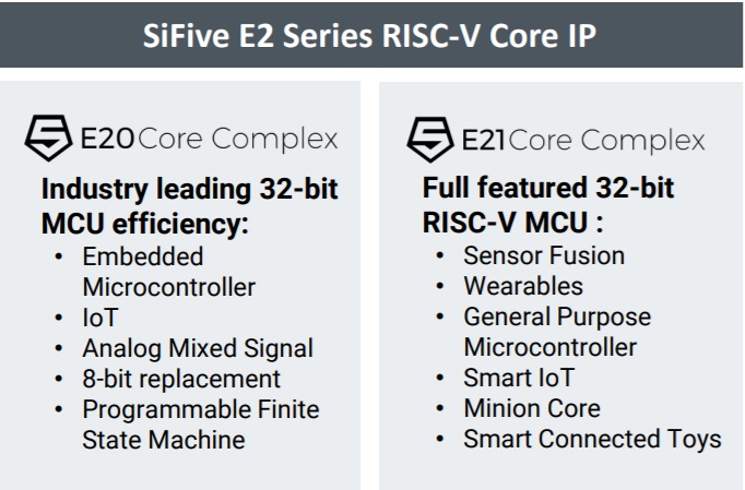
    The E20 and E21 add to the growing list of SiFive RISC-V cores addressing the embedded controller, IoT, wearables, smart toys. On June 25, DAC opening day, SiFive announced the availability of its E2 Core IP Series, configurable low-area, low-power microcontroller (MCU) cores designed for use in embedded devices. From their press release, the E2 Series extends SiFive’s product line with two new standard cores, the E21, which provides mainstream performance for MCUs, sensor fusion, minion cores and smart IoT markets; and the E20, the most power-efficient SiFive standard core designed for microcontrollers, IoT, analog mixed signal and finite state machine applications. Additionally, the company announced enhancements to its existing standard E3 and E5 Core IP Series.

    The SiFive E20 and E21 are designed for markets that require extremely low-cost, low-power computing, but can benefit from being fully integrated within the RISC-V software ecosystem. Fully compatible with the exact same software stack, tools, compilers and ecosystem vendors as other higher performance SiFive cores, the E2 Series enables these new markets to take advantage of the robust software ecosystem that has been exponentially growing since SiFive first introduced commercial RISC-V cores in 2016. Both cores are fully synthesizable and verified soft IP implementations that scale across multiple design nodes. The new product series provides a variety of new features, including a fully configurable memory map, multiple configurable ports, tightly integrated memory (TIM), fast IO access and a new CLIC interrupt controller for extremely fast interrupt response, hardware prioritization, and pre-emption.

    Furthermore, SiFive gives designers the ability to configure a SiFive RISC-V Core Series to their specific application needs, with the ability to fine-tune performance, microarchitectural features, area density, memory subsystems and more within a given Core Series. Customers can either directly leverage the silicon-proven standard SiFive Core IP like the E21 or use it as a starting point for their own customizations.

    Naveed Sherwani, SiFive’s CEO commented “I am happy to announce the availability of SiFive’s new E2 Series RISC-V Core IP. Its small area, low power, and low latency interrupt controller make it the obvious choice for many embedded applications. Like all SiFive IP, the E2 Series is fully customizable and can be configured to meet demanding high-performance applications as well as extremely low power and area sensitive applications. E2 Series evaluation RTL and FPGA images are available for free on our website.”

    “SiFive’s Core IP is the foundation of the most widely deployed RISC-V cores in the world and represents the lowest risk and fastest path to customized RISC-V based SoCs,” said Yunsup Lee, co-founder, and CTO, SiFive. “Our Core IP Series takes advantage of the inherent scalability of RISC-V to provide a full set of customizable cores for any application – from tiny microcontrollers based on our new E2 Core IP Series to our previously announced, Linux-capable, multicore U Core IP Series.”

    In addition to announcing the new E2 Core Series, SiFive also expanded its E3 and E5 Series to support coherent multicore configurations for high-performance embedded applications. In addition to multicore support, the E3 and E5 Series have a new enhanced multiplication unit which allows the E31 and E51 Standard Cores to achieve over 3 CoreMarks/MHz while still using open-source GCC compilers. The E3 and E5 Series are ideal for high-performance, real-time applications such as storage, industrial, modems, and networking.

    E Series: 32-bit and 64-bit Embedded Core IP
    E5 Series – 64-bit Embedded Core IP
    E5 Series embedded cores offer 64-bit performance at 32-bit price and area
    E3 Series – 32-bit High Perf Core IP
    High-performance 32-bit RISC-V embedded cores, the E3 Series is the most widely deployed RISC-V core in the world
    E2 Series – 32-bit Lower Power Core IP *New*
    SiFive’s smallest, lowest power, 32-bit core series. The E2 Series is optimized for deeply embedded, microcontroller applications

    U Series: 64-bit Linux-Capable Core IP
    U5 Series – 64-bit Applications Core IP
    The world’s first RISC-V Linux capable core with high performance and optimized for maximum efficiency

    When I visited the SiFive booth of the RISC-V pavilion, Drew Barbier, their Sr Applications Engineer was highlighting the E2 series capabilities. He shared with me the following insight:

    Some of the salient features of the E2 Series Memory Subsystem are:

    • The E2 core can be configured with 1 or 2 bus interfaces
    • The S-Bus is a highly optimized crossbar allowing fast access to the Tightly Integrated Memory banks (TIMs) and System Port
    • Optional parallel access support to 2 TIM banks with 2 bus interface configurations
    • Atomic instruction RISC-V support for single cycle Read-Modify-Write operation
    • E2 Core instruction and data accesses can target any Port or TIM

    The Core Local Interrupt Controller (CLIC) provides:

    • A simplified interrupt scheme allowing low latency interrupt servicing, hardware prioritization, and pre-emption
    • Extreme low latency with support for Vectoring directly to ISR (6 cycles into first ISR instruction, 18 cycles to complete a simple ISR in E2 series pipeline)
    • Interrupt pre-emption capabilities with up to 16 nesting levels, and programmable priority levels within each level
    • An easy to use programmer model with GCC interrupt function attribute and no assembly, multiple software interrupts with programmable priority levels with drivers included in the SDK

    For more information on SiFive’s RISC-V Core IP including full datasheets, specifications and app notes, visit www.sifive.com. More details on E2 can be found here. A SiFive E2 Series RISC-V Core IP Launch deck can be found here