webinar banner AI 2026 v2

Aprisa and Apogee – The New Avatars

Aprisa and Apogee – The New Avatars
by Alex Tan on 07-19-2018 at 12:00 pm

Earlier physical optimization impacts a design QoR gain and can disclose potential hurdles in dealing with unknown design variants such as new IP inclusion or new process node issues. Along the RTL-to-GDS2 implementation continuum, a left-shift move requires a robust modeling and proper context captures in order to produce meaningful outcomes.

Aside from synthesis, floorplanning, placement and routing are three major optimization segments that largely shape the final design footprint and determine the feasibility of design targeted performance. Although judging on its own merits, each has a unique set of pre-requisites and its optimization context, close alignment among them is crucial.

The floorplanning step involves applying an optimal strategy for top-level placement on the given budgeted area without incurring complication for downstream implementation steps. For example, having a robust IP or macro placement that honors a uniform data flow and accomodates adequate repeater staging area or track allocation, should provide a better chance of placement and route convergence as it will prevent congestion risk and unmanagable area increase.

Similarly, during the place and route step, preserving the optimization intent achieved in earlier synthesis and driving further gate level QoR’s (Quality of Results) is key to ensure predictability in design closure convergence.

Avatar Physical Implementation Solution
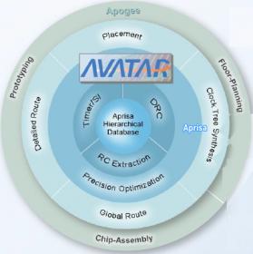
Aprisa and Apogee are two physical design related products from Avatar Integrated Systems (previously known as AtopTech). Aprisa is a complete P&R system which includes placement, clock tree synthesis, optimization, global routing and detailed routing. It has embedded analysis engines that correlates with foundry-approved sign-off tools and supports standard formats for its collaterals (Verilog, LEF/DEF, Liberty, SDC and GDS2). It has been certified for 16/14/10nm and 7nm.

Apogee is a top-down hierarchical prototyping floor planning and chip assembly tool. It enables fast analysis of design hierarchy and automates many manual tasks such as macro placement and blockage creation to ensure faster convergence to an optimal floorplan.

Both tools shares a common analysis engine and database that ensures tight correlation between block and top level timing. Avatar’s In-Hierarchy-Optimization (iHO), intended to help top-level timing closure without either the traditional black-box modeling or flattening step, is an example of many patented technologies incorporated in both tools specifically developed to address increased design challenges in advanced process nodes.

Floorplanner and Placement
Apogee handles complex floorplan criteria such as rectilinear regions, multi-height cells and mixed/overlapping sites. Both channel based and channel-less floorplans are supported. It has an automatic placement blockage generator and a macro placer with grouping and legalization capabilities. To aid for data flow analysis, the GUI has both hierarchical flyline analysis and logic-vs-layout cross-probing features. With its unified architecture and hierarchical data model, it comfortably handles multi-million gates design and easier hierarchical ECO with continued 2x to 3x runtime improvement per major version refresh.

Aprisa´s placement technology is a timing and congestion driven analytical based placer, which keeps track of real time TNS and congestion overflow –to automatically adjust timing and congestion parameters for an optimal QoR or runtime tradeoff. Aside from the standard cost factors (such as wire-length, area, leakage power, etc.), the adaptive placement and optimization engines take into account critical dependencies such as pin accessability. It has automatic neighbor rule as well as user’s controlled version to allocate cell spacing for pin access.

Aprisa features a partition-based optimization mode that allows intelligent path clustering based on timing criticality. Such method is intended to achieve a more efficient thread allocation and multi-thread scaling for subsequent optimizations. Its power optimization features include switching activity optimization, OCV aware placement, useful skew handling and always-on buffering/retention cell placement. Both UPF and CPF constraints are supported for low power-driven optimization.

MCMM Analysis, CTS and Timing Analysis
Aprisa has native and adaptive MCMM (Multi-Corner Multi-Mode) approach that automatically groups scenarios and analyzes them in mixed sequential/multi-threaded mode, yielding an optimal balance of memory usage and run time. It supports various on-chip variation methods (AOCV, LOCV, POCV and LVF).

Aprisa´s progressive MCMM CTS handles various scenarios for complex designs such as based on skew-group, slack-driven, multi-point; mesh and H-tree; power aware clock tree optimization with useful skew; cluster-based clock trees or meshes; auto clock-gate cloning/decloning, etc. The CTS engine balances clock trees for all modes and corners while allowing flexibility to leverage skewgroup information to further optimize the clocktree. The route-based clock tree optimization minimizes the use of buffers, automatically create special routing constraints (such as double-width/spacing/via, shielding, route layer, etc.) and matches latency targets given by user for any pins. It is accompanied by a GUI for visualizing, cross-probing and real-time intervention such as clock buffer resizing or moving clock buffer or leaf cell to different level of the hierarchies.

Aprisa includes a fast timing analysis engine with many advanced features. Based on Avatar rating, it takes 5 minutes per million instances. It supports SDC parsing, native OCV timing analysis, CRPR (Clock Convergence Pessimism Removal) and a timing browser
Routing
Addressing first-order effects of SI (Signal Integrity), EM (Electro Migration) and metal-fill emulation with near detail route level accuracy during global route stage is key to its success in delivering targeted detail route outcomes. Aprisa’s fast global route engine was rated to route millions of nets in minutes. It supports multi-threading and routes 250K instance in about 5 minutes on an 8 CPU machine. The global route includes track assignment that facilitate delays and signal integrity assessment.

Aprisa’s detailed router is a hybrid technology, which support both gridded routing as well as off-grid pin routing when needed. According to Avatar, unlike the other routers’ handling of DRC as an afterthought, Aprisa handles all the DRC violations during route optimization. This includes handling complex design rules (such as EOL spacing or extension, minimum enclosure, etc.), special routing rules (such as double spaced, shielding, double vias, etc.) and DFM related issues (such as wire-spreading, double-vias).

For advanced nodes, Avatar’s router uses its own patented color-aware DPT routing technology to enable DPT compliant routing and also support CM (Cut-Metal) routing methodology. As resistance is more prevalent in advanced process nodes, Aprisa’s router has the capability to minimize jogging for lowering via usage and accounts for high-R layer usage in pre-route RC estimation as well as in detail routing for better timing. It automatically promotes critical net to high-metal layer while leveraging low-resistive wire for long nets connection to reduce buffer usage. Tight timing correlation is also maintained throughout the process including between pre-route and post detail route steps.

The resurgence of Avatar’s physical design solution has added color to the IC physical implementation landscape. An integrated solution that aligns both the optimization and analysis engines while managing proper contexts using a unified data model can deliver enhanced QoR’s. Aprisa and Apogee seems to have demonstrated such leverage.
For further details please check here: Aprisaor Apogee.


A Last-Level Cache for SoCs

A Last-Level Cache for SoCs
by Bernard Murphy on 07-19-2018 at 7:00 am

We tend to think of cache primarily as an adjunct to processors to improve performance. Reading and writing main memory (DRAM) is very slow thanks to all the package and board impedance between chips. If you can fetch blocks of contiguous memory from the DRAM to a local on-chip memory, locality of reference in most code ensures much faster access for many subsequent operations which will frequently find the data/addresses they need in these cached copies. This greatly improves overall performance, despite need at times to update cache contents from a different location (and maybe store back in DRAM what must be evicted from the cache).

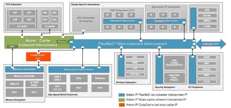
Good ideas generally get pushed harder and so it is with cache; a hierarchy of on-chip caches further reduces the frequency of needed off-chip memory accesses and further increases overall performance. This extends from level-1 (L1), small, fast and really close to the CPU, then L2 all the way up to (potentially) L3, caches at each stage being larger and slower. The last level unsurprisingly is called the last-level cache (LLC) and is generally shared in multi-processor systems. Which is why cache coherency has become a big topic. Caches are a trick to improve performance but must still maintain a common logic view of the off-chip memory space. If you work with Arteris IP, you’ll use their Ncore cache coherent interconnect for communication between IP in the coherent domain to manage that coherency. Ncore also provides proxy caches to synchronize IP in the non-coherent domain with the coherent domain; I wrote about this earlier.

However a lot of logic in an SoC does not sit in the coherent domain; after all, there’s more to an SoC than the CPUs. There’s a human interface (perhaps graphics, audio, voice control), communications, external interfaces, security management, accelerators and sensor interfaces. At least some of these components also need to access memory extensively so can also benefit from cache support. This is the need Arteris IP’s CodaCache aims to support – as a cache function for an individual IPs in the non-coherent world, or as an LLC for the non-coherent system as a whole, or both of these.

Let’s address an obvious question first; these caches are operating in a non-coherent domain, so how do you avoid coherency problems without syncing back into the coherent domain? No magic here – in the same ways you avoid such problems in any context. Address map separation is one choice; each IP writes to and reads from its own address space and there are no overlaps between those spaces.

JP Loison, Senior Corporate Application Architect at Arteris IP, told me that the cache is very configurable. It can be used purely as a cache of course, or part of it can be configured (even at runtime) to be used as a scratchpad, or the whole thing can be used as a scratch pad. This is a handy feature for those targeting multiple markets with one device, e.g. low-cost IoT not needing external memory but where you do need fast on-board memory, all the way up to high-performance image processing where you need all the performance advantage of caching. Interestingly, while the cache can sit on the Arteris IP FlexNoC (non-coherent) bus fabric, it doesn’t have to. You can connect it directly to any AXI bus and use it independently of other Arteris IP products.

Another clever thing JP mentioned you could do with CodaCache is partition the cache to alleviate congestion. Rather than having, say, one big 4MB cache block tying up routing resources around that block, you can split the cache into multiple sub-blocks, say 1MB each, which can settle around the floorplan, spreading routing demand more evenly.

JP also mention support for what he called “way partitioning”, a method to reserve cache lines for specific IDs, giving them higher priority and therefore higher performance than for other accesses. For example, one ID could reserve ways 6 and 7 in the cache for high-priority real-time tasks, another could reserve way 5 for medium priority tasks and all other IDs would have to fight it out of the remaining ways. That’s a pretty detailed level of configurability.

You can learn more about CodaCache HERE. The product was released only last month and is now in production. It has been proven already with multiple customer, per JP.


Machine Learning and Embedded FPGA IP

Machine Learning and Embedded FPGA IP
by Tom Dillinger on 07-18-2018 at 12:00 pm

Machine learning-based applications have become prevalent across consumer, medical, and automotive markets. Still, the underlying architecture(s) and implementations are evolving rapidly, to best fit the throughput, latency, and power efficiency requirements of an ever increasing application space. Although ML is often associated with the unique nature of (many parallel) compute engines in GPU hardware, the opportunities for ML designs extend to cost-sensitive, low-power markets. The implementation of an ML inference engine on an SoC is a great fit for these applications – this article (very briefly) reviews ML basics, and then highlights what the embedded FPGA team at Flex Logix is pursuing in this area.

Introduction
Machine learning refers to the capability of an electronic system to:

[LIST=1]

  • receive an existing dataset of input values (“features”) and corresponding output responses
  • develop an algorithm to compute the output responses with low error (“training”) and,
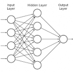
  • deploy that algorithm to accept new inputs and calculate new outputs, with comparable accuracy to the training dataset (“inference”)The common hardware implementation of the ML algorithm is a neural network – loosely based on our understanding of the electrochemical interactions in the brain among a neuron cell nucleus, its dendrites, and the axons/synapses sending electrical impulses from other neurons to the dendrites. The figure below illustrates a “fully-connected, feed-forward” neural network, a set of nodes comprising:


    • an input layer (the “features” of the data)
    • additional computation layers (zero or more “hidden” layers)
    • an output layer

    In the fully-connected (acyclic graph) architecture, the computed value at the output of each node is an input to all nodes in the next layer.


    An expanded view of each network node is shown in the figure below. The computed input values each have an associated multiplicative “weight” factor. The node calculates the sum of the weighted inputs – in vector algebra terms, the “dot product”. A “bias” value may also be used in the summation, as part of the node calculation.


    There are two importance (interrelated) characteristics of note in the neural network – “normalization” and “activation”. The numerical range of individual input features could vary widely – for example, one input could range from (-10,10), while another spans (0,1). The neural network designer needs to assess the relative importance of each feature, and decide to what extent the range should be normalized in the input layer. Similarly, this architectural decision extends to the activation function within the node, as part of the output calculation. A variety of (linear and non-linear) activation functions are in common use – a few examples are shown below, including functions that normalize the output to a specific range (e.g., (0,1), (-1,1)).


    Some activation functions include a “threshold”, such that the output is truncated (to zero) if the dot product result is below the threshold value. (The axon and endpoint synapses that connect a neuron output to the dendrites of other neurons are also capable of complex electrical filtering – the brain is indeed a very unique system.)

    At the output layer, the activation function is a fundamental aspect of the neural network design. The desired output result could be a numeric value, or could be “classified” into (two or more) “labels”. The simplest classification would be a binary 0/1 (pass or fail, match or no_match), based upon comparisons to the threshold ranges defining each label.

    Training/Test and Inference
    The selected neural net architecture needs to be “trained”. A subset of the given input dataset records is selected, and feature values applied using the existing weights and biases at each node. The network output values are compared to the corresponding “known” output values for each input record. An error measure is calculated, which serves as the optimization target. Any of a number of error models can be used – two common examples are depicted in the figure below.


    The training phase then adjusts the network weights and biases, re-submits the input training dataset, and re-calculates the error. Sophisticated algorithms are used during optimization to derive the (multi-dimensional) “surface gradient” of the error as a function of the weights and biases, typically working backwards from the output layer. The training phase iterates through multiple input data applications, error calculations, and weight/bias adjustments, until an error minimum is reached. Special techniques are employed to avoid stopping on a “local minimum” of the error response.

    Once the training phase completes, the remaining dataset records serve as a separate “test” sample. These test records are applied to the network with the final training weights/biases, and an “accuracy” measure derived. (Accuracy is perhaps best understood for classification-based outputs – did each classified result for each test record match the given label? Also, considerable ML research is being pursued to select “good” training/test subsets, as well as identify “noisy” input data that may not be representative of the final environment.)

    Once a neural network with suitable accuracy has been derived, the design implementation is ready to be deployed as an “inference engine” for general purpose use.

    Numeric Resolution
    A key finding from ongoing ML research relates to the resolution of the weights, bias values, and activation calculations. During the training phase, high resolution calculations are needed at all layers – e.g., 32-bit floating point (fp32). However, once the network is ready to use for inference calculations, a reduction in resolution may result is minimal loss in accuracy, with corresponding improvements in power/area/cost. For example, weights and biases could be transformed to fp16 or 8-bit fixed point representations at some/all layers of the network, while maintaining comparable accuracy (link) – that is a game-changer.

    ML and Flex Logix eFPGA tiles
    I had an opportunity to chat with Geoff Tate and Cheng Wang at Flex Logix about their initiatives into supporting inference engines within an embedded FPGA implementation.

    Cheng indicated, “As you may recall, our eFPGA designs utilize modular, abutted tiles, allowing customers to build the IP in the capacity and configuration best suited for their application. In addition to the logic-centric tile (comprised of programmable LUT’s), we offer a DSP-centric tile with a rich mix of multiply-accumulate functions. ML customers are seeking high MAC density, optimal throughput, and power efficiency – we have prepared an ML-centric tilewith a concentration of programmable int8 MAC’s, ideally suited for many ML applications.” (This ML tile is similar to, yet simpler than, the DSP offering. Like the DSL tile, it can be readily incorporated into a larger eFPGA block. Also, the MAC’s can be configured as 8×16, 16×8, and 16×16.)


    Cheng continued, “We are engaging with customers seeking a variety of network options – e.g., even smaller bit resolutions, unique memory interfacing for faster access to retrieving weights and biases.”

    An increasing area of ML development relates to network partitioning. For architectures larger than the physical implementation, a set of successive, partial calculations are needed, with partition weights/biases updated prior to each evaluation. The overall throughput is thus a strong function of the time to load new weights and biases. The figure below illustrates how block partitioning applies to matrix multiplication (from linear algebra).


    For ML implementations targeting IoT edge devices (with input patterns representing sensor data), network partitioning may involve dividing the overall calculation between edge and host. In these cases, a detailed tradeoff assessment is made between throughput and power efficiency/cost.

    Geoff added,“Many customers are seeking an embedded FPGA solution with an ML-optimized MAC resolution. Our implementation style enables us to offer a tailored solution for a specific process and architecture within 6-8 months. Also, we realize there are a number of ML coding libraries used to define the neural network architecture – e.g., Caffe, TensorFlow. (link – also, see Footnote) A software toolset to establish a flow from the ML code to our eFLX compiler can be made available.”

    The attractiveness of a high throughput, power-efficient, and low cost embedded SoC inference engine implementation using an eFPGA optimized for the specific resolution requirements will no doubt greatly expand the breadth of ML applications. For more information on the Flex Logix ML tile specifications, please follow this link.

    –chipguy

    Footnote: The link provided is a YouTube video of a Stanford University CS lecture describing Caffe and (especially) TensorFlow ML software libraries. The most popular class in many CS departments is no longer “Introduction to Object-Oriented Programming”, but rather “Introduction to Machine Learning”. 😀

    PS. This introductory description above depicted a full-connected, acyclic, two-dimensional neural network graph, with a set of one-dimensional vectors for weights and biases. ML research has also pursued many other complex network topologies than depicted above, include graphs with feedback connections between layers. Also, the training phase was “supervised”, in that output values/labels were assumed to be provided for each input record. Additionally, “unsupervised” training algorithms are used when the inputs do not include corresponding output data – this represents a significantly more complex facet to ML, as the “pre-training” phase attempts to identify (higher-level) features from correlations among the detailed (lower-level) inputs.


SEMICON West Intel 10nm and GF 7nm Update

SEMICON West Intel 10nm and GF 7nm Update
by Daniel Nenni on 07-18-2018 at 7:00 am

SEMICON West seemed a little slow last week but maybe it was just me. I’m sure SEMI will come out with record breaking numbers but I did not see it in the exhibit hall (see the video). What I did see was hundreds of exhibitors but I had no idea what they did. San Francisco again was very congested and smelly. I talked to a friend who is in public works and he said drugs are relatively cheap and plentiful so SF is the place to be when you run out of prescription opioids, and it is getting worse.

SEMICON West 2018 Wrap (video)

Bottom line: I am no longer in favor of SF as a destination for DAC or any other conference. Either do it in San Jose or Santa Clara or get out of Northern California! San Francisco is not going to fix this problem if we keep ignoring it.

Robert Maire, Scotten Jones, and I attended SEMICON and had very productive meetings which gave us a pretty good outlook for 2018/2019. Robert has already published, Scott will add more, and this is mine. Click on the Events tab in the navigation bar to see them all.

We met with GlobalFoundries (Gary Patten, Erica McGill, and Jean-Baptise Laloe). Interesting story about Erica. She hosted Scott and I in Malta a couple of years back where we enjoyed a clean room tour. Erica is the first communications person I have seen do the tour partly because you cannot wear make-up, perfume, hair products, heels etc… but also because it is highly technical which excludes most semiconductor communications people.

The nice thing about meeting with Gary and Erica is that they know that we know more than we should so we are treated differently than the mainstream media. Questions are answered on and off the record and we can fill in the blanks if there are any. My interest was 7nm, Scott will cover FD-SOI.

GF took a different path to 7nm than most expected. In June of 2015 the IBM/SUNY Alliance unveiled the first 7nm silicon using SiGe and EUV which was expected to be production worthy in 2017. Globalfoundries however chose a much more “TSMC like” path to 7nm. It is not plug compatible but it is close enough so customers can move from one process to another with relative ease. AMD is already doing this (straddling TSMC and AMD) and others will follow, absolutely. In my opinion 7nm will be a very long node. If history repeats, 5nm will be a half node that will be mostly skipped like 20nm and 10nm in favor of a more aggressive 3nm.

Another issue is current political problems around the world which Robert Maire spoke to at SEMICON (standing room only). Having a leading edge fab in the United States is becoming more and more favorable and having a “TSMC like” process in the United States puts GF in a unique position. According to Gary, 7nm is on track for early 2019 production which is in line with the other foundries except TSMC and Apple of course. Apple is always first to production with TSMC to make the fall iPhone launch.

Intel is on the same track with 10nm. Based on people who actually know, 10nm yield is steadily improving and should be at Intel acceptable levels by the end of the year for early 2019 mass production. Remember, Intel went through a similar exercise at 14nm. Yield delays were standard practice in the history of the semiconductor industry up until Apple joined our ranks. TSMC and Apple work jointly on a customized process that must be in production in time for the yearly iPhone launch. The trade-off made of course is performance for yield. Intel on the other hand will not sacrifice performance for yield thus the 10nm delay.

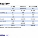
The result being that the Intel processes are faster and denser than the same named foundry processes. You can see this by comparing FPGAs from Xilinx (TSMC 16nm) and Intel/Altera (14nm). The S2C FPGA prototyping boards support both Xilinx and Intel FPGAs and we see a significant performance and density advantage with Intel 14nm. I do not expect to see Intel 10nm and Xilinx 7nm FPGAs for a year or so but my guess is that we will see a similar performance and density advantage for Intel.

The other interesting Intel news is that they may skip 7nm and move directly to 5nm. This of course is a marketing move since the Intel processes are off by a node name or two. The Intel 14nm process rivals TSMC 10nm and the Intel 10nm process rivals TSMC 7nm. Scotten Jones is the expert so I will defer to him if you need further convincing. Personally I think it is a great idea and will support Intel 100% on this one, absolutely.


Accelerated Verification with Synopsys

Accelerated Verification with Synopsys
by Alex Tan on 07-17-2018 at 12:00 pm

At DAC 2018, Synopsys held a lunch panel discussing verification challenges faced by the industry leaders, their adopted approaches and the overall verification technology trends. This panel of industry experts from Intel, AMD, Samsung, STM and Qualcomm also shared their viewpoints on what drives the SoC complexity and how their teams have tackled them and achieved successes.

From the Synopsys Verification Group, Michael Sanie (VP of Marketing) and Chris Tice (VP of Verification Continuum Solutions), kicked-off the session by highlighting the current state of Synopsys verification landscape.

As an established verification leader a TTM 40%+ emulation growth, Synopsys showcased at the DAC exhibit floor, ZeBu® Server 4. It offers a 2x emulation performance gain, 5x lower power consumption and lower cost of ownership with half the datacenter footprint. Other features include scalable capacity to 19B+ gates, 12x faster waveform data transfer vs ZeBu Server-3, architected for simulation acceleration, with 16x higher host-bandwidth vs dual PCI/e Gen3 I/F; faster compile, hybrid emulation and an advanced debug. Also dubbed as his ‘15th generation emulation system’ by Chris Tice.

HAPS-80 (High-Performance ASIC Prototyping System), Synopsys prototyping systems had 1700+ successful deployments. Newly introduced, HAPS-80 Desktop comes with built-in software and increased debug throughput.

The maturity of FGP (Fine Grain Parallelism), originally announced as Cheetah Technology (2016), then part of the standard VCS release and now available to every VCS user as VCS-FGP (2018). FGP eliminates any manual work by dividing the design into groups of events and exploits many-core processor architectures to parallelize these clustered tasks.

Also highlighted the investment made in Verdi debug format support (interactive, text, waveform based debug) and VCFormal experienced the fastest software growth in Synopsys verification group. Other summary includes SpyGlass has over 300+ customers using static verification; new features RDC and improved performance. VC Lint and VC CDC was introduced as the next generation Static technology with advanced word-level data model from VC Formal combined with rules/engines from SpyGlass (Rules, Engine) with integration compatibility with DesignCompiler and PrimeTime.


Accelerating Digital IP Verification Methodology (STMicroelectronics)
According to Mirella Negro, MCD Verification Group Manager, being a leading supplier for Smart Driving and the Internet of Things through its 32-bit general-purpose microcontrollers requires digital IP robustness, very aggressive market-introduction schedules and complex MCU verification need. STM deployed VC Formal last year, augmenting its coverage driven dynamic verification to prevent simulation iterations due to RTL refreshes, which occur between bug huntings and final coverage analysis.

Using Synopsys comprehensive formal Apps such as Property Verification (FPV), Formal Coverage Analyzer (FCA) and Automatic Extraction of Properties (AEP), STM was able to achieve faster property convergence in many scenarios. VC Formal’s broad portfolio of formal assertion IPs, also uncovered significant number of pre-silicon corner-case bugs, enabling STM to deliver more designs in less time, without compromising quality.

The native integration of VC Formal with VCS and Verdi debug engine, allows design and verification teams to easily leverage formal technologies and automate root cause analysis of formal results –such as the code unreachability issue which affect final coverage. Although some complex STM IP’s still need simulations, a growing number of IPs are validated using formal only.

Acceleration of Pre-Silicon Emulation (Qualcomm)

Senthil Dayanithi, Sr. Engineering Director at Qualcomm concurred on the continuing shift-left trend in SOC H/W development, which can be achieved through migrating to system emulation and a high-level S/W development with real peripherals.

Pre-Silicon Emulation Efficiency Improvement (Intel)
Raju Kothandaraman, Graphics H/W Director at Intel described the increasing visual experiences as driver to complexity in both design sizes and workloads. He believes that while emulation spending is growing it is necessary to efficiently use hardware to keep-up with verification complexity. The prerequisite to that is to understand the key metrics which include the following:

  • Compile time – Try to reduce bottlenecks during compile step through the use of emulation friendly RTL, the best known methods and the selection type of models. All of which could deliver 4-5x improvement.
  • Model frequency – Use emulation friendly transactors, evaluate and fix any unusually slow frequency due to long timing paths (may be attributed to timing loop). Work and collaborate with EDA vendor. A 2-3x improvement and higher model frequency can be gained here.
  • Wall clock efficiency, Utilization and Debug TAT – Improving how fast regression time, identifying inefficient DPI calls, having more offline debug capacity and local memory solution on emulator. Also key to pre-silicon validation is to have effective board packing, an enhanced debug methodology and model types, ID of right content to run. All of these could bring in 3-4x performance improvement.

His final take on gaining emulation efficiency includes a change of mindset to a more efficiency driven, knowing when to empower design versus automation, an internal cross-team partnership and external EDA collaboration.

Driving Performance and Power Tuning Presilicon (AMD)
Andrew Ross, Principal MTS from AMD stated that the basic premise of the two metrics (performance, power) is to complete more work with less time and completing more work with less energy. ZeBu emulation system has been at the center of this solution handling full SOC RTL (1B+ gates), GPU, clock domain ratios modeled for silicon accuracy and applied performance tuned register init and fusing. As part of the virtualize execution environment, the (hypervisor) VirtualBox interfaced through PCie transactors to the ZeBu box. The App running visualization (GPU) reporting # of cycles required for execution. AMD also leveraged ZeBu zDPI passive monitoring activity and fast waveform capture.

Performance analysis can be done using full S/W and H/W stack as in silicon bring-up, allowing high fidelity observability of the combined system behaviors. In summary, system level emulation solution enables power and performance analysis with real world workloads, a more data driven analysis and augmenting simulation based approaches.

Addresing Unique Verification Challenges of Era Constant Changes (Samsung)
According to Seonil Brian Choi, Master Principal Engineer at Samsung, an increased in design complexity has led to less verification and development time. Moreover, multiple specification changes triggers a redesign and subsequent verification efforts that may eventually shift the completion verification time closer to the deadline leaving no time to allocate for S/W verification.

Seonil shared the methodology evolution for verification and S/W development from simulation centric to a more system level virtual prototyping. A shift from little modeling to more modeling while enabling an early S/W development.

The takeaway from this panel session is that leading SOC’s require advanced technologies including simulation, formal verification, fast emulation, hybrid emulation prototyping, and debug to complete the challenging task of verification of such SoCs.

To watch a video of the DAC Verification Panel, visit HERE.

More 55DAC blogs


Platform ASICs Target Datacenters, AI

Platform ASICs Target Datacenters, AI
by Bernard Murphy on 07-17-2018 at 7:00 am

There is a well-known progression in the efficiency of different platforms for certain targeted applications such as AI, as measured by performance and performance/Watt. The progression is determined by how much of the application can be run with specialized hardware-assist rather than software, since hardware can be faster and consume less power than software running on a less specialized platform. At the low end are general-purpose CPUs, where the application is entirely in software, then GPUs, FPGAs, DSPs and finally custom hardware – an ASIC such as the Google TPU.

So why not just build every such solution as an ASIC, at least as long as you can justify the initial build investment? Two reasons dominate. First, the underlying algorithms may be rapidly changing (as in AI) and second the time required to design an ASIC can be significant, making it very difficult to keep pace with rapidly-changing needs. You’d have to look hard to find more fiercely competitive markets than AI applications (q.v. Facebook, Apple, Amazon, Google, Baidu, Alibaba, TenCent, and ADAS/autonomous car suppliers) and datacenters (q.v. Amazon, Microsoft, Google and others). All are working in rapidly-evolving winner-take-all markets. In these domains, time isn’t just money, it’s survival.

Which is why eSilicon is launching a platform approach to targeted applications. These ASIC platforms are augmented with libraries and infrastructure targeting AI and datacenter networking needs. Each is built on 7nm technology and is PPA-optimized as a whole to optimize for the specific needs of those domains.

Let’s start with the networking platform. This offers:

  • 56G and 112G SerDes with long-reach and short-reach architectures at 56G, to support many lanes at very high data rates, yet at the lowest power achievable
  • TCAM memory to speed route lookups, packet classification, packet forwarding and ACL commands
  • PHY to connect to high-bandwidth memory (HBM2) stacks in the package. Note incidentally that eSilicon has significant experience in building 3D and 2.5D systems, both at die and package levels. So a system-in-package solution becomes an easy choice
  • Specialized memories/memory compilers for pseudo-2-port, pseudo-4-port and other application-specific memories, providing high bandwidth with area and power saving, along with a range of I/O buffers

The AI platform (which they call neuASIC) is a little more involved. The goal here is to provide first all the IP components you would expect in a standard SoC (CPU, local SRAM, NoC interconnect, interface to external memory I/O buffers), here called the ASIC Chassis. The neural-net (NN) part of the design is implemented on a stacked layer above the chassis, with 3D interconnect to connect to the AI layer. Again, this leverages eSilicon experience in 3D packaging.

If you simply hardwire your AI architecture, it will have great PPA but you may need to replace it (build a new ASIC) as soon as a competitor jumps past you. The neuASIC structure is optimized to limit the need for redesign against algorithm changes. First the Chassis hardware should be relatively insensitive to changes in NN algorithms. Next, the AI layer is divided into tiles. This mega-cell partitioning encourages durability in the underlying hardware to changes in the NN algorithms, thanks I would assume to the natural modular style of NN designs. Each tile is built around commonly-used macro AI functions such as convolution or pooling functions, some pre-designed by eSilicon, some might be 3[SUP]rd[/SUP]-party, some may be designed by the ASIC customer.

As of May of this year, neuASIC provides a library of MAC blocks, convolution engines and memory-transpose functions as pre-built macro functions (they continue to work on more), speeding assembly of common NN structures. Since memory and operations must be very tightly coupled in NNs to reduce overall power, they also provide pseudo-4-port memories for neuron support (2 neuron data inputs, 1 weight input, one neuron output) and a specialized memory called a weight-all-zero-power-saving (WAZPS) which will zero outputs at lower power if weights are zero (but at lower power than by default), a common occurrence in NNs with sparse weight matrices.

Design is supported through a modeling system they call the Chassis Builder, through which you can model the functional operation of an NN, while also extracting PPA estimates to guide optimizing the design to your targets.

For both platforms, the goal is to provide a fast path to a working solution, while also meeting your aggressive PPA goals. Doing so requires more than a standard ASIC platform. You need to be able to put together a chassis quickly with predefined I/O ring, interconnect and high bandwidth memory access, you must have the IP/macro primitives required in those applications, those IP should be optimized together for the application and you must be able to configure and characterize your planned design to your PPA objectives. These platforms look like a good start and a promising long-term path to accelerating high-performance, low-power ASIC design in these domains. You can learn more about the networking platform HERE and the AI platform HERE.

Related Blog

Related Blog


VLSIT Conference – imec on CFETs

VLSIT Conference – imec on CFETs
by Scotten Jones on 07-16-2018 at 12:00 pm

The 2018 VLSI Technology conference was held in Hawaii in June and is one of the premier conferences covering integrated circuit process technology and circuit design. The Complementary FET (CFET) is an emerging option to continue logic scaling into the next decade. At the conference imec, GLOBALFOUNDRIES, Tokyo Electron and Coventor presented “The Complementary FET (CFET) for CMOS scaling beyond N3,”. I have copies of the paper and presentation and had the opportunity to interview one of the authors, Julian Ryckart of imec.

The mainstream technology of choice for high performance ICs is currently the FinFET. Leading foundries are ramping 7nm FinFET technologies with risk starts of 5nm FinFETs planned for next year. Looking forward, somewhere around 3nm a transition is expected to horizontal nanowire/nanosheet (HNW/HNS) technologies, in fact Samsung has already announced a 3nm “Gate All Around” technology based on nanosheets for 2021. As we look even further forward beyond the introduction of HNS, a variety of scaling issues present themselves. The CFET is an emerging concept to provide scaling by stacking devices in the third dimensions.

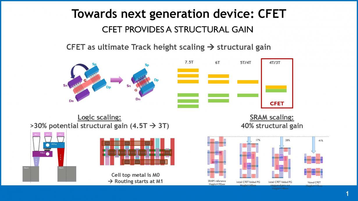
In CMOS technologies nFETs and pFETs are used in pairs so that when the nFET is on, the pFET is off or vice versa. This results in low power consumption because current only flows during switching. nFET and pFET pairs are therefore a natural primitive in CMOS logic. In current technologies the nFET and pFET devices are fabricated in the same plane, in a CFET technology the nFET and pFET devices are stacked on top of each other providing an area reduction for the same pitches. The combination of the CFET with buried power rails can reduce the track height of the cells as well and for SRAMs a 40% structural gain is seen for the same pitches. Figure 1 illustrates some of the scaling advantages of CFETs.


Figure 1. CFET Structural Advantage

The CFET fabricated in this work is a fin over fin configuration with pFET fin on the bottom to benefit from substrate induced stress and the nFET vertical sheet on the top. Due to lower hole mobility in silicon, pFETs are typically weaker devices than nFETs and need extra stress to match the nFET performance. Putting the nFET on top also makes fabrication easier because the nFET work function is a sub-set of the pFET work function.

This CFET process features separate electrodes for the nFET and pFET allowing connections to be made either up to the interconnect stack or down to the buried power rails. Figure 2 illustrates the split electrode and the buried power rail.

Figure 2. Stacked Electrodes and Buried Power Rails

The split gate CFET process makes routing easier and the routing propagates up into place and route. The ability to shift P and N connections “north and south” means that only 1D connections are needed.

The stacked devices produced by this process are comparable to conventionally fabricated FinFETs in terms of performance. Parasitics can makes one of the devices different from the other and needs to be addressed and mitigated. There are some advantages to this process that can even result in better than FinFET performance. The CFET drain extensions can be minimized reducing gate to drain parasitic capacitance and improving performance, see figure 3.

Figure 3. Optimizing CFET Performance

In a standard FinFET the middle of line is routed parallel to the gate whereas for a CFET it is orthogonal to the gate also reducing gate to drain capacitance.

The process of building CFETs shares many steps with standard FinFET processes. A CFET process doesn’t add very many steps but the steps are more critical and require better control. Fill – planarize – etch-back steps in the CFET process require precise depth control of the etch back in order to fabricate and connect to the stacked devices.

Currently CFET devices are a single threshold voltage and it is already hard to build the sperate nFET and pFET work functions. Supporting multiple threshold voltages is an unsolved problem and appears very complicated. This is however unlikely to be a show stopper for CFETs because there aren’t any sliver bullets any more and CFETs appear to be the most general-purpose solution available.

I asked Julian about stacking beyond 2 layers, I am aware of groups exploring stacking up to 7 layers and more as a long-term scaling path that could even relax pitch requirements. Julian’s belief is that 2 layers makes sense because it creates a natural primitive of CMOS, but he was difficulty seeing scaling beyond 2 layers.

Some simple cost comparisons show that CFETs provide scaling less expensively than shrinking pitches by lithography.

In summary CFETs offer an intriguing option for scaling beyond HNW/HNS processes.


Semicon Wrap Up holding pattern in turbulent air

Semicon Wrap Up holding pattern in turbulent air
by Robert Maire on 07-16-2018 at 7:00 am

The stock market hates uncertainty most of all. In the absence of the known, the market will assume the worst or close to it. Right now there is a lot of uncertainty that continues to have more downside beta than upside beta. Everybody we spoke to at Semicon wakes up in the morning wondering what tweet was sent at 5AM that will impact their part of the hundreds of billions of dollars of trade in the semiconductor market. Projects and plans are up in the air as no one has a clue which way things will go.

The other large uncertainty is the length and depth of the current slowdown related to the memory market and specifically Samsung. How many quarters will it last? Will it spread to other chipmakers? We also spoke to a number of people in the industry who are already thinking about belt tightening and other standard knee jerk reactions to a slowing business model.

To be very clear, business is still quite good, everyone is making money and will still be making good money just less of it in the future. Gone are the bad old days where the majority of the industry went underwater during a cyclical downturn. We also don’t expect as much of a levered negative reaction that we used to see in the bad old days when smaller companies and sub suppliers where hit harder than the larger companies. Even the smaller companies have gotten bigger and stronger and the inventory pipeline isn’t as big as it used to be. Simply put the downturn should not be as ugly nor as long lived as we have seen in the past.

The problem remains that we don’t have a hint of when the trade issue will resolve or the length and depth of the downturn and that lack of knowledge is likely more damaging than the actual reality when it happens.

TEL confirms second half slow down but hopeful for 2019 recovery
At the Tokyo Electron investor meeting as well as in private meetings, TEL, the second largest equipment maker after AMAT confirmed what we all already know about a H2 slowdown. Less clear is when it will recover. Right now the hope is in 2019 but there is no basis other than hope and assumption.

TEL is an obvious beneficiary of the current trade war between the US and China as even if the trade war is resolved, chip customers in China will be wary and probably have a built in bias away from US makers towards Japanese makers (which runs counter to their traditional distrust of the Japanese)

You can never get the toothpaste back in the tube…
Even if we manage to work things out in the trade war with China, we think permanent damage has already very clearly been done. US companies will be distrusted as their supply could be cut off in the time it takes to tweet.

China’s “Made in China 2025” got proven 100% correct as China clearly needs to be independent of US control and leverage. Non US semiconductor companies will benefit and China will be looking for a work around for everything they depend on. This probably also doubles the pressure on Chinese hackers to steal more IP as they are more afraid of not being able to get it legally.

Waiting on Lam…the elephant in the room that isn’t talking
Its pretty clear that Lam will likely see most of the impact of Samsung’s memory slowdown. Their absence at Semicon and lack of pre-announcement only fans investor concerns and industry speculation.

Our view is that the downside risk to the stock remains as analysts can’t really do a good job of cutting estimates with nothing to go on and will have to wait until Lam announces to adjust their estimates and targets and it will take a while for the market to absorb the changes. Others in the industry will likely breath a sigh of relief once Lam officially announces reduced numbers as it reduces the speculation on their own performance.

Avoiding the “death by a thousand cuts”
Our main hope is that Lam and other companies in the industry cut their expectations enough in this first round so that we don’t get stuck in the downward death spiral of reducing numbers every quarter until we hit bottom. Expectations need to be reset to a level where the industry can meet and exceed them without worrying. Although its hard to adjust numbers to account for trade issues and we would not expect that, we think that the industry can take a whack at re-adjusting spending in light of memory pricing and near term demand. Better to under promise and over deliver in the stock market game.

Embrace the “Cycle” ….it takes pressure off management
We think that managements who have pushed the idea that this is no longer a cyclical industry have done themselves and the industry a disservice. They can no longer shift the blame and point their finger at the cyclical nature of the industry as the culprit . Since the business is up and to the right forever it must be managements fault for any blip or bad performance for several quarters cause its no longer a cyclical industry. Embrace the cycle…its your friend and whipping boy.


AMAT talks long term AI but short term is ugly

AMAT talks long term AI but short term is ugly
by Robert Maire on 07-15-2018 at 7:00 am

We attended Semicon West Monday and Tuesday, the annual show for the semi equipment industry. Its very clear from discussions with all our sources in the industry that confirm that Samsung has put the brakes on spending on memory and that message was reinforced by declines in their expected profitability due to weaker memory pricing. We maintain that a near term shipment drop of 25% for Lam and 10%-15% for AMAT is probable.

As we have said before, it is not possible for the rate of memory spending to continue at such high levels. Although demand has remained good, pricing of both NAND and DRAM has softened even though still quite profitable for memory makers. Samsung is taking prudent steps to slow spending.

Applied had no comments about short term trends in the industry . LAM & KLA were not having events so no other near term official commentary.

AMAT had a “feel good” series of presentations about AI being a major driver for chips and therefore chip equipment but unfortunately the long term positives of AI and big data are offset by the near term negatives of slowing memory spend and China trade issues.

While we certainly agree about the great long term prospects of AI for the entire chip and chip equipment industry (not just AMAT) it is the near term issues that will drive the stocks and have been pressuring the stocks.

The end of the day was capped off with the news of another $200B of tariffs being announced on Chinese goods which is yet another salvo in the escalating tit for tat trade war. The trade war continues to worsen with no resolution or even hopes of a resolution as it does not appear that there are any effective discussions going on other than the exchange of tariffs.

Our talk about China & Trade
We had a standing room only crowd at Semicon to listen to our discussion and presentation about China, trade, technology & Taiwan. We had a number of discussions with different company managements after our presentation and its clear that nothing about China trade is clear. Everyone is confused and waiting for the next shoe to drop much like the stock market.

One rumor we heard from multiple sources is that some large companies in the industry may have either slowed or put on hold projects in China. To be clear, business is going on as usual but new commitments of significant resources may be questioned given the uncertainty.

Meeting with AMEC …the Chinese semi equipment company
We spent some time with Gerald Yin, the CEO of AMEC, the Chinese semi equipment company. They have had huge success against Veeco the long term leader in MOCVD. They also are competitive in the etch market against Lam, AMAT & TEL etc;. While today they are not a huge force in etch they have made significant in-roads in non-critical etch especially at TSMC and domestic Chinese companies. They are also used in Intel’s China fab.

They estimate that the 20 or so fab project in China could amount to $100B in spend over the next few years.

We think they are the obvious beneficiaries of the near term trade issues between the US and China. While today they are a rounding error as compared to AMAT or LAM that is not likely to remain the case as they have the potential to do to the etch business what they did to MOCVD (maybe to a lesser extent).

We think much of this damage has already been done to the industry and will only get worse if export restrictions are actually put into place.

We would remind investors that export restrictions and licenses for export of semiconductor equipment used to be the norm and were only eased over the last years as trade with China increased. Putting those restrictions back into place would be very easy and just reverting to what had been the case for a longer period of time.

AI is great…so is big data and SSDs etc…
We certainly agree with AMAT about the huge upside potential of AI on the chip and chip equipment industries. We also think that Applied has some potential advantages loosely coupled to AI versus other companies. However, we view it more as a rising tide that will raise all boats. Right now the tide is going out due to the memory slow down and the seas are very choppy due to the China trade war which could tun into a hurricane, so its hard to go out and buy AMAT stock in the face of the near term issues.

We think that AMAT might be well served to broaden out its product line or go “upstream” into the EDA business to get closer to the design source of AI and reap more benefit over the longer term. We think it makes sense for an acquisition or collaboration for AMAT to get closer to chip design.

As previously mentioned we think investors will focus on a near term 10-15% drop quarter over quarter in shipments coupled with Applied’s industry leading China exposure rather than the long term AI upside We will continue to report on Semicon after tomorrow.

More Event Blogs


Black Scholes and IC Design

Black Scholes and IC Design
by Daniel Nenni on 07-13-2018 at 7:00 am

This is the sixth in the series of “20 Questions with Wally Rhines”

From the earliest days of my childhood, I was always trying to find ways to make money – paper routes, lawn mowing, coke sales at football games – I did it all. And, except for a motorcycle I bought during junior high school when, at age 14, I could get a driver’s license in Florida, I saved most of the money. During high school, I bought my first publicly traded stock, Eastman Kodak, and fortuitously profited from the introduction of the Kodak Instamatic Camera six months later, instilling me with the dangerous idea that I had some sort of intuition for investments despite the random nature of the luck.

So it should be no surprise that, as I worked on challenging research projects in the Central Research Laboratory of Texas Instruments, I also became deeply involved in trading standardized stock options when the Chicago Board Options Exchange opened during my first year at TI. Pretty soon I was doing “butterfly spreads”, “ratio writes” and even selling “naked calls”.


This activity stepped into high gear with the introduction of the SR-52 programmable calculator, as TI tried to catch up with the HP 65 programmable calculator that was already in the market. I went to work writing programs to improve returns and reduce risk in my stock option investing program. Not long before this, Fisher Black and Myron Scholes published an article in the “Journal of Political Economy” providing a mathematical derivation to calculate the intrinsic value of a stock option. Myron Scholes later won the Nobel Prize and founded a company, Long Term Capital Management, which experienced a blowup so big that Alan Greenspan writes about the threat it posed for worldwide financial stability in his book, “The Age of Turbulence: Adventures in a New World”. I went to work implementing the Black Scholes formula on the SR-52. The formula is a complex equation so it required some effort to squeeze it into the limited memory of the SR-52 (The SR-52 cost $395 on release in 1975 which is roughly $1,847 in 2018).

Volatility data was not generally available for most stocks so my use of the Black Scholes model focused on comparisons of options with different strike prices and expiration dates, where the volatility assumed in the equation would be constant. And then I began using it for trading. My broker at Merrill Lynch became fascinated and soon many of the brokers in his office had SR-52’s.

One day I became aware of a request from the management of the Professional Calculator Department at TI for sample programs written for the SR-52 that could be used as examples to attract customers, especially for applications other than engineering. I went to a meeting and met Rob Wilmot and Peter Bonfield (now SIR Peter Bonfield, who I’ve been associated with ever since). They were excited by my options trading program and decided to run a full page add in the Wall Street Journal offering customers a free copy of the program. It was a big success and I seriously began considering a career move into financial analysis software.

As Steve Jobs said in his commencement address at Stanford, connecting the dots that will be important to your career is difficult looking forward. In this case, the connection with Robb and Peter in the Calculator Products Division, or CPD, had an interesting consequence. Later that year, a decision was made to move CPD to Lubbock, Texas because the Division was growing so fast that space needs couldn’t be accommodated in Dallas. For people like Robb and Peter, who came from the UK, both Dallas and Lubbock were near the edge of civilization so they could easily adapt to the new environment in Lubbock. But for most of the employees in Dallas, a move to Lubbock didn’t sound attractive. Lots of management slots opened up, including the job of Engineering Manager for the Division, supervising 150 engineers who designed the chips and plastic cases for calculators. I am told that someone in the Calculator Division suggested, “Wasn’t that guy who wrote the Black Scholes program some type of chip design manager in the Central Research Lab? I wonder if he would be willing to move to Lubbock?” And that’s all it took. A few weeks later, I inherited responsibility for a group of people who had to be convinced that moving to Lubbock would be a good experience.

Most amazing was the group of managers who agreed to move. Those of us reporting to Ron Ritchie, the Division VP, included:

  • Rob Wilmot – Later became CEO of ICL (the largest computer company in Europe)
  • Peter Bonfield – Later became CEO of ICL, then CEO of British Telecom and subsequently served on boards including TSMC, Astra Zeneca, Ericsson, Sony and nine other public companies including Mentor Graphics. He has 11 honorary degrees and is currently in the news because he is Chairman of the Board of NXP. He is now Sir Peter.
  • Tommy George – Later became CEO of Motorola Semiconductor
  • Kirk Pond – Later became CEO of Fairchild Semiconductor
  • Jim Clardy – Later became CEO of Harris Semiconductor and then CEO of Crystal Semiconductor which became Cirrus Logic

The Figure above is the agenda for the Consumer Products Group part of the annual TI Strategic Planning Conference held in 1978. The “M. Chang” on the agenda is now well known to most everyone in the semiconductor industry. E. Pfeiffer is Eckhard Pfeiffer who later became CEO of Compaq Computer.

The 20 Questions with Wally Rhines Series