webinar banner AI 2026 v2

Cadence Selected to Support Major DARPA Program

Cadence Selected to Support Major DARPA Program
by Bernard Murphy on 07-26-2018 at 7:00 am

When DARPA plans programs, they’re known for going big – really big. Which is what they are doing again with their Electronics Resurgence Initiative (ERI). Abstracting from their intro, this is a program “to ensure far-reaching improvements in electronics performance well beyond the limits of traditional scaling”. This isn’t just about semiconductor processes. They want to redefine the way we architect and design/implement, along with the foundations of design, pushing ideas beyond the timeframes that industry will normally consider (they’re looking at 2025-2030 horizons).

In architecture they have two programs: software-defined hardware (SDH – runtime reconfigurable hardware) and domain-specific system on chip (DSSoC – mixing general and application-specific processors, accelerators, etc). In design they have two programs: intelligent design of electronic assets (IDEA – no human in the loop layout generator, runs within 24 hours) and Posh open source hardware (POSH – hardware assurance technology for signoff-quality validation of open source mixed signal SoCs. And finally, materials and integration: 3D-SoC (3DSoC – enable > 50X in SoC digital performance at power) and foundations required for novel compute (FRANC – proofs of principle for beyond von Neumann compute architectures).

DARPA held a summit in San Francisco, 23-25 July, to launch the initiative and announce some of the winning proposals, including a joint proposal from Cadence, NVIDIA and CMU. I talked with Dr. David White (Sr Group Director of R&D at Cadence) who will be running the Cadence part of the program, which Cadence calls MAGESTIC, as PI. David has a strong background in both AI and design. He completed his doctorate in EE/CS at MIT on characterizing semiconductor wafer states using machine learning (ML) and other methods. He later co-founded the DFM company Praesagus, later acquired by Cadence, and for the last ~10 years has been running Virtuoso EAD and is also lead for the Cadence ML task force.

Unsurprisingly, Virtuoso has been leveraging ML for quite a while, so they’re not coming into this cold. And since they’re partnered with NVIDIA and CMU, this is a heavy-hitting team. David says they’ll start with analog. That’s pretty clear – they already have product on which to experiment and build. But remember the goal is ambitious – no human in the loop to generate layout – so this will take a bit more than polishing.

Interestingly, they are including intelligent PCB place and route in their goals. In placement, they will use deep learning to evaluate the possible design space and placements, select an optimal set based on analytics and previous learning, run the placement and feed metrics back to the learning engine. They’ll do a similar thing in routing, again feeding back the fitness of result to the DL engine.

David expanded further on the expected flow for custom IC design, I would guess because the foundations of this are already clear through their Virtuoso EAD and advanced node place and route capabilities. The key challenge here is to address uncertainty in design intent; how can you remove the human from the loop if what the human wants isn’t clear? We know what we want, but in a general and not fully-specified sense, and we expect to have it adapt as implementation progresses. This is where ML combined with analytics has promise; to capture implicit intent and best-practices based on what is explicitly known but also on what can be observed from legacy designs.

He illustrated their approach with a custom layout example. Locally a designer can run fast extraction and electrically-aware assistance, fast RC analysis, static EM analysis and so on. From this they can switch to a more intensive electrically-driven optimization where they can explore design alternatives aligned with intent (captured as design constraints), each of which is graded using cost functions. All of this is of course massively parallelized (server farms, clouds, etc) to get quick turn-around. This whole subsystem interacts with an intelligent tools subsystem for ML, analytics and optimization, the intelligent tools both observing the outcome of analyses and optimizations at the designer level and feeding back recommendations and refinements. Obviously this flow still has a human in the loop but you could imagine through learning, refinement and new capabilities, the need for that human could be minimized or even eliminated in some cases.

We wrapped up with a couple of questions that occurred to me. How do you bootstrap this system? David said that this is a common challenge in such systems; the standard approach is to start with baseline models, while allowing those models to adapt as they learn. Does he expect that system behaviors will diverge when applied to different applications? Yes, certainly. Baseline models won’t change but tools should tailor themselves to provide optimal results for a target application. Which raises an interesting point they may consider – might the tool be able optimize across multiple target applications, to build a product to serve multiple markets?

Kudos to Cadence for landing a role on this ambitious initiative. I’m sure the rest of us will also benefit over time from the innovations they and other partners will drive. You can learn more about the DARPA initiative HERE and Cadence’s MAGESTIC program HERE.

Autonomous Driving and Functional Safety

Autonomous Driving and Functional Safety
by Tom Dillinger on 07-25-2018 at 12:00 pm

The timelines proposed by automobile manufacturers for enabling fully autonomous driving are extremely aggressive. At the recent DAC55 conference in San Francisco, I attended a panel discussion on Functional Safety issues for assisted and autonomous driving, sponsored by Mentor Graphics. I also had the opportunity to chat with Bryan Ramirez, DVT Strategic Marketing Manager at Mentor, about the progress, opportunities, and challenges in addressing these issues. The insights shared by Bryan and the panel were eye-opening (to me, at least).
Continue reading “Autonomous Driving and Functional Safety”


Optimization and Reliability for FinFET designs at #55DAC

Optimization and Reliability for FinFET designs at #55DAC
by Daniel Payne on 07-25-2018 at 7:00 am

TSMC is the leading foundry worldwide and they make a big splash each year at the DAC exhibit and conference, so I stopped by their theatre area during the presentation from IP vendor Moortec to see what’s new this year. Stephen Crosher was the presenter from Moortec and we had exchanged emails before, so this was the first time that we had a chance to meet in person.


Designing an SoC for use in a system is a complex task these days, and even premier design companies like Apple have reported performance issues with their newest MacBook Pro laptops because as they were warming up under high loading the fans came on to cool the system off and then the CPU frequency was throttled to lower the temperature, but it was throttling back too much and actually performing slower than the previous CPU generation used. Fortunately for Apple they will issue a software fix to correct the clock throttling issue. Modern day SoC projects require that the design team have a plan for an optimized system that is also reliable.


MacBook Pro overheats, throttles frequency too much. Source: Apple

Some of the challenges in FinFET design are well known:

  • Higher thermal density
  • IR drop and PDN (Power Delivery Network) issues
  • Noise between coupled signals and injected into the substrate
  • Reaching timing closure

With each successively smaller process node we enjoy the benefits of increased gate densities, but at the expense of also increased power densities that can cause reliability issues. Narrower and higher-resistance interconnect layers impact timing to a greater degree and increase the variation effects. Add up all of these issues and it makes reaching timing closure even more difficult.

The Moortec approach to these challenges is to provide monitoring IP placed strategically within certain regions of an SoC, where the PVT sensors communicate to a controller that can then perform actions like scale the voltage, or throttle clock frequencies in order to have a reliable chip. Experts at Moortec have engineered this IP across multiple process nodes:

  • 40nm
  • 28nm
  • 16nm
  • 12nm
  • 7nm

Some of the benefits of using this pre-built monitoring IP in your next chip include a reduced risk of failing to meet specs, an improved yield at the foundry, better reliability and chip lifespan, and no up-front development costs to design and qualify your own IP. With the Moortec IP embedded you can better implement dynamic or adaptive schemes like DVFS (Dynamic Voltage Frequency Scaling) or AVS (Adaptive Voltage Scaling).

Many chip segments will benefit from embedded monitoring:

  • Datacenter – thermal management, high gate densities, leakage currents, CPU temperatures
  • Consumer – process variability, thermal management, localized process variability
  • Automotive – reliability and thermal management, real-time monitoring throughout vehicle lifetime
  • IoT – edge devices that sense and monitor, manage multiple supply levels to meet power specs

Moortec has been an IP Alliance Member with TSMC since 2010, starting at the 40nm process node, and in 2016 they received a partner of the year award from TSMC. At DAC there was news from Moortec about supporting the 40nm ULP CMOS technology, useful for the IoT marketplace. It was fun to meet the Moortec team in SFO and see their customer list continue to grow with tier one clients in diverse industries.


Moortec team at DAC in SFO

Related Blogs

About Moortec
Established in 2005, Moortec provides compelling embedded subsystem IP solutions for Process, Voltage & Temperature (PVT) monitoring, targeting advanced node CMOS technologies from 40nm down to 7nm. Moortec’s in-chip sensing solutions support the semiconductor design community’s demands for increased device reliability and enhanced performance optimisation, enabling schemes such as DVFS, AVS and power management control systems. Moortec provides excellent support for IP application, integration and device test during production. Moortec’s high-performance analog and mixed-signal IP designs are delivered to ASIC and System on Chip (SoC) technologies within the consumer, mobile, automotive, high performance computing and telecommunications sectors. For more information, please visit www.moortec.com, follow us on Twitter and LinkedIn.


Automotive is setting the goalposts for next generation designs

Automotive is setting the goalposts for next generation designs
by Tom Simon on 07-24-2018 at 12:00 pm

Automotive applications are having a tremendous influence on semiconductor design. This influence is coming from innovations in cloud computing, artificial intelligence, communications, sensors that all serve the requirements of the automotive market. It should come as no surprise that ADAS and autonomous driving are creating the majority of the push in each of these areas. At DAC this year in San Francisco there was plenty of buzz about all things automotive. I was able to attend a very informative lunch event hosted by Synopsys – “Automotive Drives the Next Generation of Designs”.

The event was kicked off by Synopsys VP of Automotive Business Development, Burkhard Huhnke. There were presentations by each of the four panel members, representing a wide swath across the industry. First off there was Jonathan Colburn, Distinguished Engineer at Nvidia. He was followed by Dr. Akio Hirata, Chief Engineer at Panasonic. Next up was Hideki Sugimoto, CTO at NSI-TEXE. Last came an informative presentation by Tom Quan, Director of OIP Marketing at TSMC. The panel included chip makers, IP providers and foundry representation.

There were several important themes from the talks. Initially Burkhard spoke about the motivation for ADAS and Autonomous driving. Apparently 84% of accidents are caused by human error. So, while we cannot completely eliminate all these accidents with automation, this is low hanging fruit for improving safety. With over 100 people a day being killed in car accidents, reducing the accident rate is a goal we should pursue. In addition, there is a strong economic argument for reducing accidents, they have direct and indirect costs that go into the hundreds of billions of dollars per year.

Several speakers pointed out independently that the need for automation is greatest specifically for the least complex and most complex driving tasks. These are the occasions where humans perform most poorly. An example of a complex driving task is merging onto a busy freeway or turning at intersections. The least complex driving situations are those where distraction or loss of attention can occur, such as on long-distance trips or in traffic jams.

Nvidia, Panasonic and NSI-TEXE all talked about the changing needs for computing. Heterogeneous computing is universally considered the optimal solution for training and recognition functions. NSI-TEXE sees a large role for flow computing in offering the quickest response time for emergency events or system failures. Nvidia, as you might expect, touted the advantages of mixing GPUs with CPUs. One interesting twist that Jonathan mentioned was that Nvidia uses some of their gaming technology to modify training data to alter the conditions and create realistic, but hard to recreate training scenarios. It’s a given that the quantity and quality of training data has a big effect on the quality of recognition operations. Using real world physics, they can create virtual training data. As a result, Nvidia can generate massive numbers of hours of training data that simply would not be available in any other way.

In the TSMC talk, Tom Quan spoke about their efforts to support the automotive market. By 2020 the electronics in most cars will shift from the passive safety, infotainment and vehicle control categories to an expanded set that also includes many new functions. There will be big changes in autopilot and ADAS. New communications capabilities will include 4G/5G, V2X and over the air update. The help the environment and improve efficiency there will be greener engine controls for EV and HEV. To help drivers, there will be natural interface for voice command, gesture control and recognition tasks that could include driver alertness detection, personalization based on face recognition. These new categories will incorporate more and more TSMC technologies.

Infotainment is using 28nm and 16nm, ADAS and partial autonomous is using 16nm, and highly autonomous will require 7nm which will be prevalent after 2020. One particular area of interest for TSMC in the automotive market is sensor technology. Many cars already have 7 to 21 sensors, including multiple LIDAR, camera, radar, ultrasound and NIR camera units. Higher levels of automation will see the need for sensors to expand significantly. NSI-TEXE pointed out that the sensor data will require increased processing to extract every bit of useful information to make autonomous driving systems more reliable. Key TSMC technologies used in the sensor domain include MEMS, eNVM and high voltage processes such as BCD.

I can really only skim over the interesting content from this talk. Fortunately, Synopsys has posted a video of the lunch session. I highly recommend watching the entire session for more insights into what Synopsys, TSMC, Panasonic, Nvidia and NSI-TEXE are doing in the automotive space. Every time I attend a session like this on the topic of automotive electronics I come away with a better understanding of this rapidly changing area.


Innovation in IoT

Innovation in IoT
by Bernard Murphy on 07-24-2018 at 7:00 am

There is some interesting work reported this month in the Communications of the ACM, on novel sensing, multi-purpose uses for existing sensors and new ideas in agricultural IoT. The article opens on a method called Hitch-hike to use back-scatter methods for communication; I confess this doesn’t interest me so much, so I won’t spend any time on it (epistola mea, regulae meae).

VitalRadio is a novel approach from MIT to monitor breathing and heartrate without need for any wearable device. Your smart home can check up on you, even while you’re sleeping. I think that’s very cool. Having to wear or carry a device can be problematic for very young or very old people (e.g. forgetting to wear the thing), they can be uncomfortable (if you’ve ever used a medically-approved sleep monitor, you’ll know what I mean) and you can easily forget to charge them, not such a problem for a fitness monitor but more problematic for a medically-required device.

VitalRadio monitors your breathing and heart rate through phase variations in radio reflection. It is able to distinguish reflections from different objects through a method borrowed from radar detection; using this it can separate multiple mostly-stationary subjects, separated by at least 1-2m, and can easily extract phase variations due to inhalation and exhalation, per subject. Heartbeats appear as a smaller modulation on top of this extracted wave. The method has limits of course – it can’t distinguish pets from humans and it doesn’t work so well when a subject is moving.

Another idea called Caraoke builds on the existing e-toll transponder in your car. These are already widely-used for access to toll roads, some bridges and express lanes, and now there is interest in using them to pay at fast-food drive-throughs and parking garages. The Caraoke folks see potential in readers being deployed more widely, to track cars at intersections for adaptive traffic light control, on street lights to track speeders, for automatic parking billing for street parking and more.

A challenge in this approach is that apparently existing transponders are quite simple, assuming only one communication at a time (hence the directional antennae); they have no MAC protocol to manage multiple potential requests. An obvious solution would be to replace all of this infrastructure with more sophisticated comms, but that would be expensive. Caraoke provides an easier path. It allows continuing use of existing transponders (no need for car owners to replace these) while requiring the readers be upgraded to more intelligently handle potential collisions and extract more from the information they gather – counting cars, localizing them and estimating speed.

Clever idea. Upgrading everything to much more effective LTE or Wi-Fi communication would of course solve the technical problems and allow for all kinds of monitoring and services. But in the real world, technology alone is often not enough. Practical solutions have to bow to economics and latencies in changing infrastructure. Solutions that can build on existing tech have a definite appeal.

Finally, FarmBeats introduces a system for farm-wide data-driven optimization. IoT use in agriculture is not a new idea but this seems to be a more integrated solution than I have seen and certainly has some serious backing (Microsoft, MIT, UW, Purdue, UCSD and 6-month deployments in two active farms). The system gathers data from fixed cameras and drones, soil sensors and temperature and humidity monitoring in food storage and animal shelters.

A big part of FarmBeats seems to be ensuring reliable communications between IoT outposts and a central gateway at the farm. Some of this is intelligently duty-cycling components of the base-station to allow for cloudy weather (yeah, real clouds). Farmers are increasingly using solar power which obviously is a variable resource under these conditions. So FarmBeats builds weather forecasting into planning when power demand can be accommodated from different parts of the system.

It also controls flight paths for UAVs based on wind patterns (which can vary widely over a farm). Which makes the batteries last longer, requiring less frequent maintenance. They have some nice pictures integrating camera images of a piece of farmland with soil moisture sensing, pH sensing and ground temperature sensing (based on a surprisingly sparse set of sensors). All individually perhaps commonplace, but integrated together at this level, this starts to look like a total solution for a farmer.


Keeping Pace With 5nm Heartbeat

Keeping Pace With 5nm Heartbeat
by Alex Tan on 07-23-2018 at 12:00 pm

A Phase-Locked Loop (PLL) gives design a heartbeat. Despite its minute footprint, it has many purposes such as being part of the clock generation circuits, on-chip digital temperature sensor, process control monitoring in the scribe-line or as baseline circuitry to facilitate an effective measurement of the design’s power delivery network (PDN).
Continue reading “Keeping Pace With 5nm Heartbeat”


FDSOI Status and Roadmap

FDSOI Status and Roadmap
by Scotten Jones on 07-23-2018 at 7:00 am

FDSOI is gaining traction in the market place. At their foundry forum in May, Samsung announced they have 17 FDSOI products in high volume manufacturing (you can read Tom Dilliger’s write up of the Samsung Foundry Forum here). At SEMICON West in July, GLOBALFOUNDRIES (GF) announced FDSOI design wins worth $2 billion dollars in revenue with $1 billion dollars booked in 2017 and another $1 billion dollars in revenue booked in the first half of 2018. With the emergence of FDSOI I thought it would be useful to review who the players are in the market and what their current and planned processes look like (I recently did a similar leading-edge analysis for FinFETs available here).

FDSOI Ecosystem
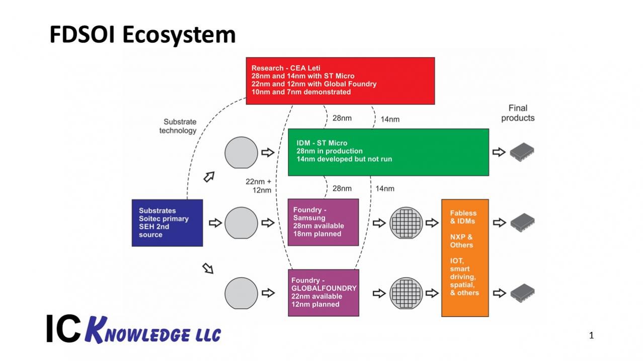
The FDSOI Ecosystem is illustrated in figure 1.

CEA Leti has served as the key research group in the development of FDSOI working with ST Micro on 28nm and 14nm processes and working with GF on 22nm and 12nm processes.

FDSOI requires engineered substrates with very thin single crystal silicon layers on buried insulator layers to insure the channel region is fully depleted. The primary supplier of FDSOI substrates is Soitec with SEH as a second source (I have written more on Soitec and their FDSOI substrates here and have another article on Soitec due to be published shortly).

The companies producing FDSOI processes are ST Micro as an IDM with 28nm in production, Samsung foundry with 28nm in production and 18nm planned, and GF foundry with 22nm in production and 12nm planned.

Figure 1. FDSOI Ecosystem

ST Micro
ST Micro introduced 28nm FDSOI in 2012 that is produced in their Crolles II – 300mm wafer fab. The 28nm FDSOI process offers a 32% to 84% improvement in performance over ST Micro’s 28nm bulk process. ST Micro also developed a 14nm process with CEA Leti but it is not in production. ST Micro has reportedly begun working with GF on GF’s 22FDX FDSOI process so long-term ST Micro may not continue to produce their own FDSOI and may move to a fabless model for this technology. Crolles II is a relatively low capacity 300mm fab and ST Micro makes other things in the fab, so FDSOI volumes are likely not large.

Samsung
Samsung licensed ST Micro’s 28nm FDSOI process and used it to create Samsung’s 28FDS process. 28FDS entered production in 2015 and is producing 17 high volume products as previously mentioned. An 18nm follow-on process is in development and due next year.

28FDS provides fmax >400GHz for RF applications, embedded MRAM nonvolatile memory and is automotive qualified. 28FDS has a 1.0 volt Vdd.

18FDS is planned for 2019, it features a back end taken from Samsung’s mature 14nm FinFET technology and provides a 35% area reduction from 28FDS. 18FDS also provides a 22% performance improvement and 37% power reduction from 28FDS. The Vdd for 18FDS is 0.8 volts.

Samsung has significant foundry capacity and can ramp FDSOI to very high volumes as needed.

GLOBALFOUNDRIES (GF)
GF’s 22FDX process entered production in 2017 and offers a 400GHz fmax, embedded MRAM nonvolatile memory and is automotive qualified. 22FDX can operate down to 0.4 volts for low power applications. There are four versions available offering, low power, high performance, low leakage or RF & analog. 22FDX is based on ST Micro’s 14nm process for the front end and the back end is optimized for cost with 2 double patterned layers and the balance of the layers being single patterned.

A follow-on 12FDX process was originally due in 2019 but GF is holding off introduction of the process because customers are just now designing and ramping up products on 22FDX. Development of 12FDX is proceeding well and it will be introduced when needed, we estimate this will be around 2020. 12FDX will offer 20% performance improvement over 22FDX.

GF is producing 22FDX in their Dresden fab and has significant capacity in place. A fab being brought up in China will also become a source for FDSOI capacity in the future.

Comparison
Figure 2 compares the process density metrics for GF, Samsung and ST Micro. In terms of the current FDSOI offerings, GF’s 22FDX is the clear leader in density and also offers the lowest operating voltage. Samsung’s planned 18FDS process will likely be slightly denser than GF’s current FDX22 process but GF’s planned 12FDX process will once again establish GF as the clear FDSOI density leader.

Figure 2. FDSOI process comparison

One thing I have a hard time understanding is why Samsung isn’t more aggressive on operating voltage. Power consumption is proportional to the operating voltage squared and FDSOI is targeted at many low power applications. GF has a clear lead in low power operation with their 0.4 volts Vdd.

Discussion
FDSOI is being positioned as a lower cost alternative to FinFETs for IOT, automotive and mobile applications. The specific FDSOI process choices in terms of density and number of interconnect layers position them to be less expensive than the denser FinFET processes. FinFET processes are also typically not well suited to analog and RF applications. We believe that at the same node and number of metal layers FinFET processes and FDSOI processes are similar in cost but once again the FDSOI processes are positioned differently, for example GF offers 22FDX with 8 metal layers as a lower cost alternative to their 14nm FinFET process that has 11 or more metal layers. 22FDX has a lower mask count than 14nm FinFET and has lower cost per wafer, the 14nm FinFET process is denser and better suited for large – high-performance designs but 22FDX offers lower cost, nearly as good digital performance and better analog and RF performance at lower power.

FDSOI also offers the unique capability for back biasing to set threshold voltages and tune performance and power consumption. Accessing the back gate for back biasing only requires a 1% area penalty while delivering a unique and useful capability not available in other processes.

FDSOI also offers lower design costs than FinFETs with 28FDS and 22FDX offering similar design costs to 28nm bulk whereas 14nm FinFET processes have design costs that are roughly 2x the design costs for 28nm bulk. 7nm FinFET design costs are expected to be even higher than 14nm design costs.

Conclusion
We believe that FDSOI is well positioned to capture market share in IOT, 5G, and automotive applications. FinFETs will continue to be the technology of choice for applications with a lot of digital logic and that require the highest possible performance. After many years of development FDSOI is poised to become a main stream alternative.


SEMICON West – Soitec is becoming a key enabler

SEMICON West – Soitec is becoming a key enabler
by Scotten Jones on 07-22-2018 at 7:00 am

A variety of growing and emerging segments of the semiconductor industry rely on Silicon-On-Insulator (SOI) wafers. Soitec is the primary source for SOI wafers particularly on 300mm. On Tuesday at SEMICON I got to sit down with Bernard Aspar, Soitec’s Executive Vice President, Communication & Power BU and Christophe Maleville, Soitec’s Executive Vice President, Digital Electronics BU and discuss what is going on at Soitec.

During SEMICON GLOBALFOUNDRIES announced they have reached $2 billion dollars of design wins on their 22FDX FDSOI platform that relies on wafers from Soitec and Soitec was clearly pleased by this development.

I started the interview by asking about Soitec’s financial health. A few years ago they were struggling. Soitec built significant 300mm capacity to support IBM’s partially depleted SOI (PDSOI) business. At one time all three major game console manufacturers relied on IBM PDSOI process for their main processor chips. Unfortunately, the value proposition of PDSOI wasn’t very good and all three console manufacturers moved away from PDSOI taking away the major driver of 300mm SOI. Last year at SEMICON West Soitec said they had returned to profitability and that has continued into this year. Over the last three years Soitec has refocused on their core business and they are now growing nicely (4% and 31% the last two years), in fact there are reports in the industry of SOI shortages.

I asked Soitec about their current capacity situation and they said the 200mm line is full and 300mm is significantly loaded. Siotec has 200mm and 300mm lines in France, a 300mm line in Singapore and a 200mm line at Simgu China. Capacity is currently tight but Soitec is investing in expanding capacity. They are contracting with their customers and contract customers aren’t suffering but if someone new wants large capacity it would take time. 300mm has grown 2x in the last two years. Soitec has >1.5 million wafers per year of 300mm shell capacity that is >50% equipped. Singapore will ramp up 300mm to follow market demand. 200mm is >1 million wafers per year.

RFSOI
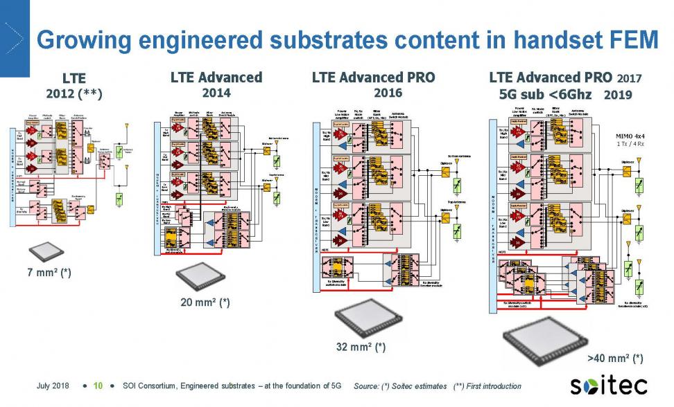
IBM’s Burlington Fab is the leader in RF SOI for antenna tuning and switching in the front end of cell phones replacing more expensive GaAs solutions. With the acquisition of the IBM semiconductor operations by GLOBALFOUNDRIES more attention is being paid to this business. Each generation of cell phones, 2G, 3G and 4G required a new and more complex front-end while maintaining the front-end module from the previous generation for backwards compatibility. With 5G on the horizon even more complex 5G front-end modules will be added to phones along side 2G, 3G and 4G modules, see figure 1.

Figure 1. Mobile phone front ends.

GLOBALFOUNDRIES has recently repurposed their 300mm East Fishkill fab for RF and Silicon Photonics and is also introducing RF into their 300mm Singapore Fab. This provides Soitec with a nice long-term growth driver for RF SOI wafers in 200mm and 300mm.

FDSOI
The recent design wins announcement from GLOBALFOUNDRIES is another example of the growing acceptance of FDSOI. Where PDSOI married an expensive SOI substrate with a complex process and provided only moderate performance improvements, FDSOI offers a greatly simplified process to offset the expensive starting substrate. FDSOI also combines good logic density and performance with low power and excellent RF and analog performance. Both Samsung and GLOBALFOUNDRIES have FDSOI foundry processes currently available and next generation processes in the works (I will be writing more about this shortly). 5G and Internet Of Things (IOT) are two emerging applications where FDSOI is expected to be very successful. FDSOI is made on SOI wafers with very thin silicon layers of ~6nm on ~20nm buried oxide layers. Soitec has significant intellectual property in producing these demanding specifications with the required uniformity.

Silicon Photonics
Silicon Photonics has been in development for many years and is starting to gain traction. The need for very high speed/energy efficient data transport in datacenters is driving an effort to move optical interconnect down to the blade level creating significant unit volume. This is an emerging opportunity for Silicon Photonics (I will be writing more about Silicon Photonics in the near future). 5G is another emerging application for silicon photonics. Silicon Photonics processes are fabricated on SOI wafers with ~500nm silicon layers on 1 to 3 micron buried oxides.

Piezzo Layers
Soitec’s expertise in wafer bonding and thinning is also being applied to creating thin piezoelectric material layers on insulator (POI) for filter applications. The emerging 5G standard has tight signal specifications that need well controlled stable filters providing another application for Soitec’s core expertise.

Other Applications
Soitecs basic tool box of bonding and controlled layer thickness can also be applied to thicker SOI layers for power electronics. Bonding of novel III-V materials is another area where Soitec can apply their expertise to produce novel engineered substrates. For example, they can produce thin InGaAs layers on sapphire for micro display applications.

Figure 2 illustrates the different Soitec substrates to support the applications discussed above and figure 3 illustrates how the various substrate types support 5G.

Figure 2 Soitec substrate options.

Figure 3. Soitec engineered substrates 5G usage.

Soitec – Leti Partnership
During SEMICON West Soitec and Leti announced the creation of a Substrate Innovation Center at Leti. Leti is a long-time pioneer in the development of SOI. The new center will bring together Soitec and Leti’s expertise with equipment vendors to drive further innovation with a prototyping line that can explore new processes that can’t be developed on active production lines.

Cost
Cost was at one time a big stumbling block for SOI adoption and I asked if SOI prices are still coming down. They replied that price has come down to no longer be a blocking point to go into foundry. New products come at a price in-line with value added. The standard 15 years ago was a GaAs front end for mobile phones, but then RF SOI provide a 2x cost reduction. FDSOI substrates are more expensive but provide simpler processes and solutions so they are cost competitive. SOI is not the severe price pressure/blocking point it once was.

Conclusion
Where Soitec was at one time reliant on PDSOI going into game machines, the company now has a portfolio of products addressing, automotive, wearables, mobile and cloud. With Soitec’s engineered substrates becoming a key enabler in these segments, Soitec is well positioned for sustainable growth.


Maximize Bandwidth in your Massively Parallel AI SoCs?

Maximize Bandwidth in your Massively Parallel AI SoCs?
by Daniel Nenni on 07-20-2018 at 12:00 pm

Artificial Intelligence is one of the most talked about topics on the conference circuit this year and I don’t expect that to change anytime soon. AI is also one of the trending topics on SemiWiki with organic search bringing us a wealth of new viewers. You may also have noticed that AI is a hot topic for webinars like the one I am writing about now.

We have been working with NetSpeed for 3 years now and have published blogs covering a wide range of topics. You can see their landing page here. NetSpeed has done some of the best and most widely viewed webinars that we have been involved with and I expect this one will be the same.

How do you maximize bandwidth in your massively parallel AI SoCs

Tue, Jul 24, 2018 8:30 AM – 9:00 AM PDT

When designing a SoC for AI applications, you are faced with a system using 1000’s of cores in a massively parallel architecture. Performance, bandwidth and quality of service (QoS) are critical requirements and the challenges of meeting them are very different for these SoCs used for AI. This webinar, in 30-minutes brings out the challenges and the solutions that has empowered multiple leaders in the AI space.

John Bainbridge, Principle Application Architect, NetSpeed Systems, will be presenting. Before joining NetSpeed John worked for Qualcomm on the SnapDragon chips so John knows SoCs, absolutely.

I have an advanced copy of the slides and they are definitely worth a look. Here is a quick outline:

Breaking down the AI workflow:

  • How it happens
  • What matters
  • Critical use cases
  • SoC Data FlowArchitectural Challenges:
  • Large number of cores
  • Extremely high bandwidth
  • Peer-peer traffic and multicast
  • Sophisticated QoSBottom line: Traditional approaches are inadequate for AI SoCs.

    John then goes into the NetSpeed approach, technology, and QoS support. This is why I like webinars, you get to hear it from and interact with the experts. Not as good as live but definitely the next best thing. Register even if you can make the live event so you automatically get a link to the replay. I hope to see you there!

    About NetSpeed
    NetSpeed Systems provides scalable, coherent on-chip network IPs to SoC designers for a wide range of markets from mobile to high-performance computing and networking. NetSpeed’s on-chip network platform delivers significant time-to-market advantages through a system-level approach, a high level of user-driven automation and state-of-the-art algorithms. NetSpeed Systems was founded in 2011 and is led by seasoned executives from the semiconductor and networking industries. The company is funded by top-tier investors from Silicon Valley. It is based in San Jose, California and has additional research and development facilities in Asia. For more information, visit www.netspeedsystems.com.


TI Patent Priorities

TI Patent Priorities
by Daniel Nenni on 07-20-2018 at 7:00 am

This is the seventh in the series of “20 Questions with Wally Rhines”

Probably the most innovative person I met at Texas Instruments, other than Jack Kilby, was Ken Bean. Ken had a list of patents that would impress even the most skeptical. He started his career at Eagle Picher and came to TI in the mid 1960s. He was a warm, delightful and modest person but very innovative when it came to finding solutions for silicon manufacturing problems. He worked in Semiconductor Group Product Divisions as well as research labs over his TI career, as did Mike Cochran, a topic that I’ll address later.

Ken Bean almost never saw a semiconductor manufacturing problem that he couldn’t solve. When TI had problems introducing the “thermal printer” that was used in the “Silent 700”, Ken had a solution that made the silicon print heads manufacturable. One of the most innovative patents that Ken filed was the patent on the slicing of silicon wafers. Easy, don’t you think? No. Ken addressed a problem for DUF (or diffusion under film) in bipolar integrated circuits. “Pattern shift” was a problem that occurred because early bipolar integrated circuits used wafers that were oriented to or crystal planes. As a result, subsequent layers of deposition “shifted” modestly as the epitaxial layer grew in the direction of crystal orientation. This caused a shift in the alignment of subsequent photomasks. Not a problem for Ken. He was called in to solve the problem and he did. Why not slice the wafers a few degrees off the perfect orientation. Then the DUF layer wouldn’t follow the crystalline orientation. It worked. Subsequently, wafers for bipolar integrated circuits were sliced slightly away from perfect orientation.

In the early 1970s Monsanto decided to get out of the semiconductor wafer business and showed up at TI with a list of patents for which they hoped to claim royalties (since TI still manufactured its own polysilicon and silicon wafers). After Monsanto showed their patents, TI lawyers passed Ken Bean’s patent to them, showing why wafers used for bipolar semiconductors are sliced a few degrees away from the perfect orientation (https://patents.google.com/patent/US3379584A/en). The story goes that the Monsanto lawyers looked at the patent and closed their brief cases. That was the last that the TI lawyers saw of them. It was truly a fundamental patent in the early days of semiconductor history. I loved my interaction with Ken and he loved our family. To his death, he communicated, kept our Christmas cards on his refrigerator and delighted in the success that TI ultimately achieved.

One of the things that Ken taught me was the importance of customer interaction in the innovation process. Ken had assignments in the Semiconductor Group and in the Central Research Labs as well as the Semiconductor Research and Development Lab. Interestingly, he generated patents at approximately the same rate per year regardless of where he was working. The same was true of Mike Cochran, who worked in a variety of organizations in TI, including both semiconductor product groups and research laboratories (and is partially responsible for the Cochran-Boone patents on the microprocessor). I decided to analyze the patent productivity of the truly great patent generators like Ken and Mike. Fortunately, TI had a system that helped me. After the TI DRAM lawsuits, TI management decided that patents were a very important source of royalty revenue, much to the dismay of many TI engineers who had been taught that patents should only be used defensively, to allow TI to enter new markets. So TI created a special segment of the annual performance review process that rewarded the creators of the most valuable patents. Those lawyers who negotiated the patent cross licenses voted on the most valuable patents. The result: I now had a list of the most “valuable” patents.

The result of the analysis amazed me although I wasn’t allowed to publish the results. But the conclusion was clear. People like Ken Bean and Mike Cochran generated about the same number of patents per year. But the ones that they generated when they were in product groups turned out to be much more valuable than those they generated when they worked in research organizations. Why? I concluded that, because the patents they filed when they were in product groups were developed in response to a customer problem, they grew in value as more competitors adopted similar solutions to the same type of problems. The other patents sounded great; they just weren’t as valuable because they were generated by innovative ideas rather than customer problem solving.

The 20 Questions with Wally Rhines Series