webinar banner AI 2026 v2

AMS Experts Share IC Design Stories at #55DAC

AMS Experts Share IC Design Stories at #55DAC
by Daniel Payne on 08-01-2018 at 7:00 am

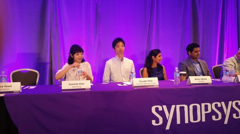
At #55DAC in SFO the first day is always the busiest on the exhibit floor, so Monday by lunch time I was hungry and took a short walk to the Marriott hotel nearby to listen to AMS experts from several companies talk about their EDA tool use, hosted by Synopsys:

  • Samsung
  • Toshiba Memory Corp.
  • NVIDIA
  • Seagate
  • Numem
  • Esperanto

Continue reading “AMS Experts Share IC Design Stories at #55DAC”


Verification Importance in Academia

Verification Importance in Academia
by Alex Tan on 07-31-2018 at 12:00 pm

“Testing can only prove the presence of bugs, not their absence,” stated the famous computer scientist Edsger Dijkstra. That notion rings true to the many college participants of the Hack@DAC competition offered during DAC 2018 in San Francisco. The goal of this competition is to develop tools and methods for identifying security vulnerabilities in the SoC designs using both third-party IP (3PIP) and in-house cores. The trustworthiness of such SoCs can be undermined by security bugs that are unintentionally introduced during the integration of the IPs.

During a 6-hour final trial, the finalists are requested to identify and report security bugs from an SoC that is released to them at the start of the day. The teams mimic the role of a security research team at the SoC integrator, in trying to find the security vulnerabilities and quickly dispatch them back to the design team –so they can be addressed before the SoC goes to market. The bug submissions from the teams are then scored in real time by industry experts. The team with highest score is declared as winner.

At the end of the competition, both Hackin’ Aggies from Texas A&M University and The Last Mohicans from IIT Kharagpur were both declared as winners. I had a subsequent interview with Professor Michael Quinn from Texas A&M, who has been actively shepherding the school’s team to take part in the competition and also joined by the Cadence staff who are coordinating the university programs: Dr. Patrick Haspel, Cadence Global Program Director of Academic and University Programs and Steve Brown, Marketing Director of Verification Fabric Products. Some excerpts from the Q&A session are included in the second half of this article.

DAC and Verification Engineers

Based on DAC 2015-2017 statistics, about 38% of the attendees are engineering professionals and about 10% are academia as shown in figure 1. Although there are other venues such as IEEE sponsored events that involved the academia, their participation in the industry sponsored events such as DAC or DVCon could be viewed an indicator for how much participation or interest is given in the ecosystems. Based on a subset of the statistics, verification engineer attendance consistently ranks third after CAD/application and design engineers (see figure 2).

A well rounded verification engineer demands proficiency in both the design implementation aspects as well as the functional verification techniques. We are accustomed to college programs providing training to be design engineers, computer scientists and process engineers –but no so much tailored for a verification engineer. This prompts the question on how we should prepare these professional candidates to be more adaptable to the industry requirements?

Cadence Academic Ties
Aside from their own R&D dollars, EDA companies innovate through the various synergistic partnerships among its ecosystems’ members, including their customers and the academia. Being at the forefront of the EDA ecosystem, Cadence has actively fostered a strong relationship with the academia through the Cadence® Academic Network program, which facilitates the exchange of knowledge by co-organizing educational events or trainings and providing access to the latest Cadence technologies. There are several notable subprograms related to this venture as tabulated here:

Interview with Professor Michael Quinn

Texas A&M University has been part of Cadence Academic Network Program and ranks first in Texas in term of student size. The university launches the 25-by-25 initiative, which targets an engineering enrollment of 25,000 by 2025 and this year boasts largest freshman female engineering class in the country. Its electrical and computer engineering programs recently were ranked 12th and 10th among public universities.

The following excerpts are from Q&A session with Professor Quinn:

Could you comment on current research emphasis in the area simulation/verification?
“From the verification standpoint, the biggest area getting looked at is associated with security. Texas A&M has a whole new department that has grown up for the past few years, very well endowed and it’s about security design, architecture and also verification. I think their biggest push in these area is in formal. Formal based approaches, not so much functional,” Prof. Quinn said. “By the way, we did (the contest) without using the formal tool,” he quipped.

Which Cadence tools do you use?
“My class uses all the simulation and visualization tools such as Xcelium. It starts just as an engineering verification job, with a specification planning using Cadence VPlanner. The students start developing the verification environment using Cadence UVM based methodology, which is superb as it supports the current IP design methodology,“ said Prof. Quinn. It also allows the students to incrementally do a bottom-up verification and integration works, starting with low-level IP and progressing to the SOC level. A key strength of such approach is the ability to seamlessly reuse of works previously applied at the lower-level. Subsequent verification and debug involves running random testings and the use of Vmanagerto tie various aspects of planning, testing, tracking and analysis together. And finally Indago, to efficiently manage debugging process.

Should the school program be geared towards software development mastery, hardware design proficiency or hands-on applications for EE candidates?
He believes we need all the above. A more well rounded designer is being looked for by companies and can be transitioned to different projects. Along this end, he aspires of having more courses that are inter-disciplinary, experiential in nature –and are based on multi-faceted curriculum that put together logic designers, architect plus software folks– would greatly enhance the learning experience.

What is the current state of engagements with Cadence?
Since its start in 2016 when only a handful of verification engineers entered into the industry from Texas A&M, the program has now contributed 100 or more. “It’s a win-win solution,” he said. Relating to his Drexel almamater, he believes the value of having a co-op program as good training ground for the incoming graduates. His wish is to be able to continue the efforts further and share his instructional works with an expanded network.

According to Dr. Haspel, part of the Cadence Academic Network team responsibilities is to connect the industry need of trained engineers and to enable students to not only learn but to be valuable also to the prospective employers. This is achieved through working with university on curriculum aligning, partnering with school that have the right mindsets to collaborate and arm them as the recruiting targets. Furthermore, he said “Sometimes it is the pipeline thing, but it is also the responsibility of the ecosystem…”

What is your impression on DAC presentations with respect to HW design?
Prof. Quinn is intrigued by the conference advising EDA vendors to pay more attention to big data, machine learning, security and data analytics. He concurs that it is the right feedback. He anticipates that post-silicon is able to contribute in the verification, which previously was not possible as data does not stop at tapeout. One may need a coverage monitoring –possibly at customer site by doing workload monitoring and feedback the simulation process. It is a big close-loop.

As the famous quote goes –“Tell me and I forget, teach me and I may remember, involve me and I learn.”– at DAC 2018 the Texas A&M team had demonstrated a slice of the fruitful outcomes from the EDA industry collaboration with academia. Kudo to Cadence and the Aeggis! Experiential learning really makes a difference.



Webinar: Differential Energy Analysis for Improved Performance/Watt in Mobile GPU

Webinar: Differential Energy Analysis for Improved Performance/Watt in Mobile GPU
by Bernard Murphy on 07-31-2018 at 7:00 am

May want to listen up; Qualcomm are going to be sharing how they do this. There is a constant battle in designing for low power; you don’t accurately know what the power consumption is going to be until you build it, but by the time you’ve built it, it’s too late to change the design. So you have to find methods to estimate power early on, while using that information in a way that won’t compromise your design choices because you were judging their impact based on eyeballed numbers.

This can appear difficult, particularly for RTL-based power estimation, which typically shows variance of around 15% on final gate-level estimates. Surely judging optimizations based on such coarse estimates would be very challenging unless the changes deliver massive advantages, greater than that margin of uncertainty?

In fact the picture is much better if you do differential analysis – comparing the difference in predicted power savings for different optimizations. While absolute power estimates carry that larger level of uncertainty, differences between estimates can be much more accurate for a fairly obvious reason. Differences subtract out many of the unknowns in absolute RTL power estimates: detailed cell and designware mapping, placement, routing, clock tree details and so on. What you’re left with can be much closer to equivalent differences based on signoff power numbers.

The people who build mobile solutions know more than almost all of us about squeezing out every last pico-watt of power. Apple isn’t likely to tell you what they do, but Qualcomm is just as good for learning about best practices in this domain.

Register HERE to learn more in this webinar on August 23[SUP]rd[/SUP] at 9am PDT

Summary:
Mobile devices demand high performance in a very constrained environment. As a leader in perf/watt, Qualcomm® Adreno™ GPUs, a product of Qualcomm Technologies, Inc., leverages many effective methods to improve power efficiency. In this regard, Qualcomm has developed a differential energy analysis methodology based on ANSYS PowerArtist to identify the power optimization opportunity in GPU. This methodology can help to locate the inefficient part that needs further optimization in the pre-silicon stage. Experimental results based on identifying unnecessary register toggles demonstrate the effectiveness of this proposed methodology.

Speakers:
Preeti Gupta, is head of RTL product management, for the ANSYS semiconductor business unit.

Yadong Wang is currently a staff engineer in the GPU system power team at Qualcomm Technologies, Inc., San Diego, California. He has about 10 years of ASIC low-power design experience. At Qualcomm, he is responsible for power modeling and analysis of Adreno™ GPUs, and explores and develops many effective methods to improve power efficiency. Before joining Qualcomm, he worked as a hardware power engineer at NVIDIA. Yadong earned an M.S. degree in electrical engineering from Tongji University (Shanghai, China) in 2009.

About ANSYS
If you’ve ever seen a rocket launch, flown on an airplane, driven a car, used a computer, touched a mobile device, crossed a bridge, or put on wearable technology, chances are you’ve used a product where ANSYS software played a critical role in its creation. ANSYS is the global leader in engineering simulation. We help the world’s most innovative companies deliver radically better products to their customers. By offering the best and broadest portfolio of engineering simulation software, we help them solve the most complex design challenges and engineer products limited only by imagination.


Machine Learning Meets Scan Diagnosis for Improved Yield Analysis

Machine Learning Meets Scan Diagnosis for Improved Yield Analysis
by Tom Simon on 07-30-2018 at 12:00 pm

Naturally, chips that fail test are a curse, however with the advent of Scan Logic Diagnosis these failures can become a blessing in disguise. Through this technique information gleaned from multiple tester runs can help pin down the locations of defects. Initially tools that did Scan Logic Diagnosis relied on the netlist to filter locations for various faults. This made it possible to exclude a number of potential locations. In the push to improve the so called “resolution” of the diagnosis, the tools started considering layout information. This went a long way toward narrowing down the list of potential fault locations.

When layout information was added to the mix, there was enough information to use the same data for yield analysis. However, even with the improved resolution in the number of suspects, the results from the diagnosis-driven yield analysis were not good enough. The engineers at Mentor realized that there was more information to be gleaned from the root cause analysis that comes from the test data and the design itself. What normally happens is that a number of potential root causes are identified and the probability of each one is reported. Each different failure will have a unique distribution of these potential root causes.

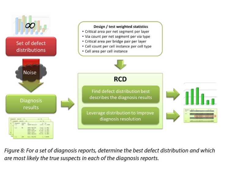
Mentor developed a technique called Root Cause Deconvolution (RCD) to help improve the fault location prediction. Mentor has a white paper on how RCD works and what kind of results it can provide. For a baseline, they conducted a simulated experiment to show how effective root cause prediction normally is. They injected two different types of single defects in different locations in a total of 470 devices. Without RCD the predicted root causes included 49 types of faults. Even the prediction of the second most probable root cause was not correct. They saw 47 probable root causes that did not correspond to any actual root cause.

When they ran with RCD the predictions narrowed dramatically down to just three root causes. This is a pretty significant improvement. RCD uses critical area information and then examines the design in detail to come up with probable root causes and their defect distributions. This data is then used to compare observed defects with the statistical information computed from the design. For realistic numbers of actual root causes the computation needed can rapidly explode. When using direct computation, even when considering only a few hundred root causes, the computational needs approach infinity. However, Mentor realized that machine learning can be used to help determine the number of relevant defect distributions that are worth looking at. It should be pointed out that machine learning is continuously finding new applications in the EDA space. This is not the first time that Mentor has decided to rely on machine learning to solve tough problems to deliver breakthrough results.

What is most interesting about RCD, as incorporated into their Tessent Diagnosis and Tessent YieldInsight, is that no additional data is required beyond what is normally needed for layout aware diagnosis. Also, in cases where diagnosis reports are encoded to protect proprietary information, the flow still works. Whenever RCD is used there are fewer probable root causes to look at, making resolving yield issues a much faster process. Because RCD’s design analysis actually can predict failure distributions in advance of failure analysis, it can open doors to more proactive yield enhancement. To learn more about how the entire process works, read the white paper entitled Leveraging Volume Scan Diagnosis Data for Yield Analysis that is available from the Mentor website.


Deep learning fueling the AI revolution with Interlaken IP Subsystem

Deep learning fueling the AI revolution with Interlaken IP Subsystem
by Daniel Nenni on 07-30-2018 at 7:00 am

AI is revolutionizing and transforming virtually every industry in the digital world. Advances in computing power and deep learning have enabled AI to reach a tipping point toward major disruption and rapid advancement. However, these applications require much higher performance and bandwidth requiring new kinds of IP and that brings us to Open-Silicon and the Interlaken IP.

Open-Silicon, a founding member of the Interlaken Alliance formed in 2007, launched the 8[SUP]th[/SUP]generation of Interlaken IP core supporting up to 1.2 Tbps bandwidth last year. This high-speed chip-to-chip interface IP features an architecture that is fully flexible, configurable and scalable.

The Interlaken IP subsystem originally developed for networking applications is enabling high speed chip to chip interface for deep learning SoCs. Open-Silicon’s eighth-generation Interlaken IP supports up to 1.2Tbps high-bandwidth performance and up to 56 Gbps SerDes rates with Forward Error Correction (FEC). Interlaken IP is a scalable, high-speed chip-to-chip interface protocol that builds on the channelization and per-channel flow control features of SPI4.2, while reducing the number of chip I/O pins by using high-speed SerDes technology, similar to XAUI. Open-Silicon’s ILKN FEC IP core meet the requirements Interlaken protocol to significantly improve bandwidth by enabling high speed SerDes integration. The FEC can easily achieve a BER (Bit Error Rate) of 10-15, which is required by most electrical interface standards using high speed SerDes built upon a flexible and robust architecture.

The updated Interlaken specification is capable of supporting SerDes beyond 30Gbps and up to 58Gbps—this was mainly because of the introduction of the peer-to-peer service, which allows sending more data on fewer lines. This led to development of Open-Silicon’s eighth generation Interlaken IP core, supporting up to 1.2 Tbps high performance and up to 56 Gbps SerDes rates with Forward Error Correction (FEC) https://www.open-silicon.com/open-silicon-ips/interlaken-controller-ip/

Key Features:

  • Fully-programmable SerDes lane mapping
  • Interlaken-LA 4-channel protocol
  • Up to 56 Gbps SerDes support
  • 1.2 Tbps high-bandwidth performance
  • Interlaken Retransmit Extension support

Standard Features:
In addition to the key features highlighted with the latest release, the Open-Silicon Interlaken IP also provides the following feature set as part of the standard IP functionality:

  • Support for 256 logical channels
  • 8-bit channel extension for up to 64K channels
  • Independent SerDes lane enable/disable
  • Support for SerDes speeds from 3.125Gbps to 56 Gbps
  • Configurable number of lanes from 1 to 48
  • Flexible user interface options:
    • 128b: 1x128b, 2x128b, 4x128b, or 8x128b
    • 256b: 1x256b, 2x256b, 4×256, or 8x256b
  • Programmable BURSTMAX from 64 bytes – 512 bytes
  • Programmable BURSTMIN from 32 bytes – 256 bytes
  • Simultaneous In-band and Out-of-Band flow control
  • Programmable calendar
  • Built-in error detection and interrupt structures
  • Configurable error injection mechanisms for test-ability

“Open-Silicon’s Interlaken IP Subsystem delivers the bandwidth scalability and performance we require for various artificial intelligence applications that require high speed inter-node connectivity. The Interlaken IP subsystem is extremely configurable and robust, which enables the high-bandwidth efficiencies required for deep learning SoCs.”-Open-Silicon Customer

Since 2007 Open-Silicon’s Interlaken IP has been deployed in several different tier-1 networking and computing customer products. Many of these products are shipping in production today in the latest technology nodes in multiple foundries. The unique flexibility and configurability built into Open-Silicon’s Interlaken core meets not only today’s technological requirements, but remains fully compatible with older designs.

Want to get a budgetary quote for Interlaken ASIC? Please fill out the Design Requirements Form.

About Open-Silicon
Open-Silicon is a system-optimized ASIC solution provider that innovates at every stage of design to deliver fully tested IP, silicon and platforms. To learn more, please visit www.open-silicon.com


Samsung Memory is easy come easy go but for how low?

Samsung Memory is easy come easy go but for how low?
by Robert Maire on 07-29-2018 at 8:00 am

Lam Research (LRCX) reported a great June quarter coming in at $3.126B in revenues and $5.31 in EPS easily beating the street’s $3.06B and EPS of $4.94. However no one will care as guidance for the September quarter is for $2.3B in revs and EPS of $3.20, way, well below the already downward revised estimates of $2.77B and $3.88.

As we had suggested in our preview notes, most analysts had underestimated the extent of the down turn in business. Guidance is well below even the lowest estimate on the street of $2.55B in revs and EPS of $3.53. We had projected a 25% decline which is exactly what management is guiding to.

At this point our thoughts turn to how long the down cycle will last and how much further down it will go?

This begs the question as to whether the slow down started by Samsung will spread to other memory makers and if foundry/logic will recover?

We think that most analysts will again underestimate the length of the down turn. In our years watching the industry we can’t think of very many downturns that were only one quarter or two quarters in length which suggests that we won’t get a recovery until 2019 at best. We highly doubt that Samsung would hit the breaks so hard for only a one or two quarter delay as the underlying issues are longer than that.

We would imagine that other memory makers will be wondering about their capex spending as well. We are in an uncertain period with many variables many of which are negative.

September low point or trough?
Management stated that it viewed the September quarter as the low point for the year. We are somewhat dubious of this given the history of the industry and our view that it seems strange for Samsung to hit the brakes so hard if they were just going to start spending again in a quarter or two.

Perhaps business from other customers can be pulled in such that some of the Samsung shortfall is made up. Management was careful not to predict timing of an uptick or length of the downturn.

How long the down turn?
If September is the “trough” the next question is how long do we stay at the trough? Its clear that there were push outs out of the September quarter and push outs out of 2018 into 2019.

We could be looking at a flat December quarter versus September with a recovery some time in 2019.
One issue we have is that logic/foundry has not been strong and in fact has been weak and not likely to make up for any memory weakness.

We listened very closely to the call and management carefully avoided suggesting an up December quarter but instead talked about long term generic positive platitudes.

There is no specific evidence that points to a recovery at this point but management has planted a flag in the ground to “call” a bottom (if only for 2018).

Single digit WFE growth
It now looks like 2018 WFE capex growth will be in the single digits. Much of this number will be determined by H2 performance which is obviously down in September but unknown beyond that. Its still too early to call 2019 and management also refrained from that prediction.

The stocks
We could see a relief rally as management’s spin is that the worst is behind us. We would caution that just as this downturn was a surprise so could we be surprised by either another leg down or a longer than expected time to recovery.

We are very dubious about those that will suggest that this is only a one quarter blip that we will quickly recover from as that is not anywhere near the norm for the industry and seems to belie the sharpness of the downturn.

We remain cautious on the group in general and more specifically memory related stocks. If we saw a big jump in the stock price we might take some money off the table before the euphoria subsides and reality kicks back in….


Daniel’s #55DAC Trip Report

Daniel’s #55DAC Trip Report
by Daniel Payne on 07-29-2018 at 7:00 am

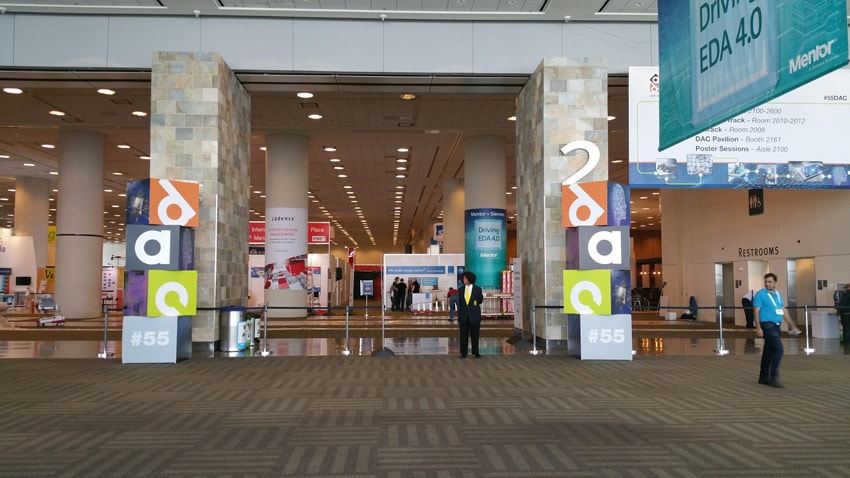
Another year, another DAC, and last month it was #55DAC in SFO and the first thing that I noticed was that the event was no longer located in the traditional North or South Halls, rather we were in the smaller, Moscone West on two floors, almost like a 3D FinFET. Checkin to get my badge was highly automated and oh so fast, well done.
Continue reading “Daniel’s #55DAC Trip Report”


1-on-1 with Anirudh Devgan, President, Cadence

1-on-1 with Anirudh Devgan, President, Cadence
by Tom Dillinger on 07-27-2018 at 12:00 pm

At the Design Automation Conference, no one is busier than an EDA company executive — conference panels, product launch briefings, customer meetings, and corporate dinners all place considerable demands on their time. I was fortunate enough to be able to meet with Anirudh Devgan, President of Cadence, at the recent DAC55 in San Francisco. His insights into the challenges and opportunities ahead for the EDA industry were most enlightening. Below is a summary of our brief Q&A discussion.

What big challenges are customers currently facing? How is Cadence positioned to address these challenges?

Anirudh said, “There are three traditional areas that customers continue to emphasize. First is PPA and design productivity. We continue to invest significantly in point tool development, building upon our parallel processing architecture. This applies across the product portfolio. Tool developers are focused on improvements to the quality of results and tool throughput.”

“The second area of emphasis is verticalization. Many customers seek to leverage our vertical design platforms. We provide broad platform support for packaging tools, analog/mixed-signal and custom design, and digital implementation.”

“And, the third area focuses on a system view. There are two axes to chip-package-system (CPS) design. One axis represents the electrical and mechanical analysis requirements of complex product designs. We have established a partnership with MathWorks, to provide unique and differentiating analysis capabilities between MATLAB and Simulink with Cadence AMS and PCB platforms. The other CPS axis relates to system software verification – our Palladium emulation and Protium prototyping platforms provide the requisite system software validation throughput.”

(For more information on the Cadence-MathWorks integration, please follow this link.)

In addition to these three areas, what are other key initiatives underway? There’s lots of buzz here at DAC about machine learning (ML), both the hardware design opportunities for different end markets, and the potential for ML optimizations within EDA platforms.

Anirudh replied, “ML will be the mother of killer apps. The market opportunities are tremendous. Consider that Google and Facebook are essentially ad companies, applying their expertise in search engines to transform a significant share of the $300B Total Addressable Market (TAM) to online advertising. The TAM for the automotive industry alone exceeds $3T, for which there are a multitude of ML applications.”

“In my opinion, there are three main pillars in science – the science of place, the science of pace and the science of pattern, or the 3Ps – which, throughout the years has followed and been enabled by advances in mathematics, physics, and more recently, computing. The science of place evolved from the understanding of the principles of advanced geometry and lasted for centuries. The science of pace is built upon the introduction of differential calculus with the corresponding understanding of dynamic systems. We are entering the onset of the science of pattern. Our ability to identify and learn from information patterns, and then adapt systems accordingly, will have an indelible impact on society. ML will be the enabler for this transition in industrialization.”

How has the resurgence of ML impacted R&D at Cadence?Anirudh highlighted, “We are embedding optimizations within our tools – commonly referred to as ‘ML inside’. For example, we are realizing PPA improvements within our Innovus implementation platform, while maintaining the same user/flow interaction.”

“We are collaborating with customers on ‘ML outside,’ to realize productivity and throughput improvements in their flows.”

What are some of the new ML areas you’re pursuing?

Anirudh said, “The opportunities for ML optimizations in the area of HW/SW co-design and verification are great.”

There’s also lots of buzz at DAC about the availability of cloud-based computing resources for EDA applications. Cadence made a major announcement, identifying multiple available environments – the Cloud Passport model (customer-managed), the Cloud-Hosted Solution (Cadence-managed), and the Palladium Cloud offering. I know we’re about out of time – can you briefly review these cloud opportunities?

Anirudh summarized, “For some time, cloud resources have been a boon to managing the IT infrastructure for many companies who have migrated HR and Finance operations. We knew our investment in a new tool architecture enabling parallel processing and distributed computing would be a great fit for cloud resources. We have collaborated with Amazon, Microsoft, and Google to enable our ecosystem on their cloud platforms.”

“Security is obviously a key concern to customers evaluating a transition of some of their workload to the cloud. We evaluated the security features and partnered with TSMC to conduct extensive security audits, which led to an endorsement in our announcement.”

“We currently have customers who have adopted either the Cadence-managed or customer-managed resources model as well as the Palladium Cloud solution.”

Indeed, the confirmation of foundry support for a cloud model should hopefully alleviate any anxiety about data security. I meant to ask a few more questions about the cloud announcement, such as “How should customers evaluate the costs and ROI of transitioning workload to the cloud?” and“Are customers investigating thecloud-based insurance for risk management?” . But alas, Anirudh had to depart.Our discussion left a strong impression on me, to wit:

  • Execution of the EDA computational workload on the cloud is a solved technical/security issue. The transition of a percentage of the overall computational workload – or perhaps to support a “burst” mode demand near tapeout – is an economic decision.


  • The dual axes of ongoing PPA and throughput improvements with ‘verticalization’ of HW/SW system design and verification requirements present tremendous opportunities for EDA growth.

and,


  • ML may indeed be the “mother of all killer apps.”

To paraphrase a Chinese philosophy, “We are indeed living in exciting times.”

-chipguy


Stubbornness Captures an Entire Disruptive Technology and Leads to an Academy Award

Stubbornness Captures an Entire Disruptive Technology and Leads to an Academy Award
by Daniel Nenni on 07-27-2018 at 7:00 am

This is the eighth in the series of “20 Questions with Wally Rhines”

In 1972, I joined TI and was assigned to work on a new contract that had just been awarded and badly needed staffing. The U.S. Department of Defense had decided that solid-state charge-coupled device (CCD) image sensors were going to be a strategic technology and they formed a joint services program under Larry Sumney (who later became CEO of the Semiconductor Research Corporation for more than thirty years). Fairchild had hired Gil Amelio from Bell Labs and was promoting buried channel technology because of its high efficiency, i.e., by using ion implantation to shift the minimum of the electrical potential to store charge below the surface of the silicon, any losses due to surface state interactions were minimal. Meanwhile, RCA was a clear contender in this emerging business because of their experience with video cameras and associated technology (as was Sony, but Sony could not be funded by the U.S. DoD).

TI was desperate to be included in the contract shootout, so they proposed a totally different approach, building the CCD on a silicon wafer and then thinning the devices from the back side to about a 25-micron thickness. This approach avoided the losses associated with shining light on the front side of the device where polysilicon and metal interconnect interfered with light transmission. The CCD thinning technology was relatively simple. We used wafers with a 25-micron thick, lightly doped p-type epitaxial layer on top of a heavily p+ doped substrate. The p-layer served as an etch stop leaving the 25-micron paper-thin layer. TI’s proposal looked good to the Navy’s Night Vision Lab for use in “Starlight Scopes” and, at the last minute, TI was added to the contract. Today, virtually all solid-state imagers are illuminated from the back side of the silicon but that approach really didn’t take off for thirty more years.

Meanwhile, Dean Collins, who ran the CCD Imaging Branch was able to promote the technology to other branches of the government, and lots of additional funding was generated for TI. One particularly difficult contract called for building a moving target indicator that would store and compare successive images. Larry Hornbeck took on the task but stubbornly refused to fabricate the device as originally proposed. Instead, he pursued what he called a stratified channel CCD architecture, the first-ever CCD to have the capability for storing two overlying charge-storage and transport channels. With the assistance of people like Ken Bean (discussed in the last blog) for the epitaxial process development and Jerry Hynecek (inventor of TI’s virtual-phase CCD) for the modeling task, Larry proved the concept with backside illumination of thinned, packaged devices.

Dean sold another program to the DoD, this time for a “solid state light modulator” that again relied on TI’s thinning expertise. It used a hybrid manufacturing process to produce a frontside, deformable mirror spatial light modulator, with backside CCD-addressing. The deformable mirror was a continuous sheet of a metalized polymer membrane. Once again, Larry came up with a different approach, consistent with his future habit of taking on the management to pursue approaches that ultimately proved to be superior and more manufacturable on the path to his “Digital Micromirror Device” or DMD. Larry was convinced that creating arrays of individually-addressable cantilever micromirrors along with a monolithic manufacturing process would solve problems of defects in the array and lead to much improved optical performance. By this time, I had taken on the job of President of the Data Systems Group and Tom Stringfellow, who managed the Peripheral Products Division of the Group, began funding Ed Nelson to support a potentially revolutionary approach to printing using the digital micromirrors. George Heilmeier, who was one of the first senior TI managers to be hired from outside the company, became VP of Research for TI and supported Larry for the chip development. By 1986 Larry had developed and patented the first practical methods for manufacturing high-density arrays of micromirrors on an integrated circuit in a conventional wafer fab. This IP and its sound reduction to practice by Larry served as an initial barrier to potential competitors who would have immediately started developing their own version of the digital micromirror device, once it was publicly disclosed in 1988. Thirty-one years after the invention of the digital micromirror device in 1987, TI is still the only manufacturer of this disruptive technology, a highly unusual, and possibly unique, example in semiconductor history.

Larry made a pivotal decision in 1987 to attach the micromirrors to torsional suspensions and actuate them into contact with rotation stops. This made it possible to manipulate light with the precision of time division by pulse-width modulation, increased the optical efficiency and reduced the address voltage. And so, the digital micromirror device (also DMD) was born (U.S. Patent 5,061,049, Spatial Light Modulator and Method, Inventor L.J. Hornbeck). The DMD became commercially known as the DLP chip.

The tiny mirrors of this device assumed a “1” or “0” position and pulse width modulation was applied to control the pixel intensity, a method that required extensive algorithmic development to produce high quality projected images. Numerous other problems had to be solved, such as the gradual increase in surface stiction to the point where a mirror would stick in a “1” or “0” position, a problem Larry immediately addressed with a novel, electro-mechanical release mechanism and in 1990 with a surface treatment that he developed (despite his claim that he hated chemistry).

Through all this, the Semiconductor Group didn’t want to take the product to production. Potential applications, like projection TV, would require major investments with questionable business benefit since the light modulator component was a small part of the total system cost. But TI, with some government help, provided enough funding to keep it alive and Larry’s persistence provided the momentum.

And then, in the late 1980s, Jerry Junkins became CEO of TI. Jerry was looking for a semiconductor project with system implications that could make a real difference to the company. Jerry’s background was running the defense business of TI and the DMD looked good to him. So, he redirected the staff of an older (four inch) wafer fab that was destined to be shut down and totally dedicated it to working out the bugs in the DLP chip.

TI built a total portfolio of know-how, software, CMOS-based manufacturing technology and intellectual property to lock up an amazingly disruptive technology. The entire motion picture industry distribution structure was totally changed as its 115 year old projection systems were replaced by “DLP Cinema” technology and software based distribution of motion pictures. TI approached other applications including printing and home projection systems with a solutions approach that included the basic DLP component, algorithmic development, manufacturing, and application engineering. The revenue approached $1B, and companies like Samsung and RCA introduced televisions based upon the DLP because of its extremely bright, sharp colors.

Ultimately, Larry Hornbeck, the innovator and developer of the technology, was nominated for and received an Academy Award of Merit (Oscar statuette) in 2015. Most interesting to me, however, is the fact that TI kept the DLP program alive for almost twenty years before any real revenue was realized. This wasn’t the only example of persistence at TI, accompanied by tolerance for inflexible innovators, and it is part of the reason that TI is the only semiconductor company that has ranked among the ten largest since the 1950s.

The 20 Questions with Wally Rhines Series


Low Cost Power NB-IoT Solution? Fusion F1 DSP based Modem!

Low Cost Power NB-IoT Solution? Fusion F1 DSP based Modem!
by Eric Esteve on 07-26-2018 at 12:00 pm

Supporting NB-IoT requires low cost (optimized silicon footprint) and ultra-low power solution to cope with IoT device requirement. Cadence Fusion F1 DSP IP has been integrated in modem IC by two new customers, Xinyi and Rafael, gaining traction in NB-IoT market. These design-win builds on previous momentum: software GPS solution from Galileo announced at MWC 18 (Barcelona) and CommSolid NB-IoT modem, at MWC 17 (before CommSolid acquisition by semiconductor company Goodix in Feb 2018).


Fusion F1 DSP architecture has been optimized to offer Ultra-low Energy for IoT Applications. These applications are multiple, as they allow connecting “things” and processing whichever data the thing is capturing. The DSP is intended for sensing, wake-up processing, audio voice speech processing and support communication with the outside world. The communication protocol can be NB-IoT, Wi-Fi HaLow or GNSS. Speech processing capabilities range from speech recognition or pre-processing to audio playback. Wake-up processing supports Voice trigger, Face trigger or Gesture trigger. Sensing can be pedestrian dead reckoning, biometric monitoring or sensor fusion.

Tensilica® Fusion F1 DSP Base Architecture is Xtensa Base ISA, offering Dual-issue, VLIW processor based on HiFi 3 DSP architecture VLIW, which is only used when required to save power consumption. MAC support is highly flexible, from Single 32×32, Dual 32×16, Dual 24×24 or Dual 16×16. To reduce MAC latency, an optional mode allows certain instructions to have a reduced latency to save power and area.

The Fusion F1 DSP core is above pictured and the green box is the core basis. Because Tensilica want to address various applications, IoT and even more, the flexibility has been the driver for the architecture definition. The 7 blue boxes (FPU, AVS, AES-128, 16-bit Quad MAC, Viterbi, Soft Bit Demap and Bit Manipulation) are proposed as pre-verified and proven option. A chip maker can really optimize the DSP core definition in respect with the real needs of the application, and minimize the DSP area and power consumption. This flexibility is added to the natural DSP flexibility, as you can use the same core to support the communication protocol (the modem) when active, then switch to support sensor fusion when needed. This strategy is also good for power consumption optimization, which is key for this type of application.

This Fusion DSP can target technology nodes from 55 nm, 40 nm, 28 nm to 22 FD-SOI (all of these sounding good for IoT applications), and obviously smaller nodes when designing to support very complexes platforms.

Tensilica® Fusion F1 DSP Value Proposition is to provide Ultra-low Power Processing for Always-On/Wearables/IoT.

The first goal is to offer leading low power DSP/Control performance. Starting with lowest possible energy for always-on and excellent control code performance (up to 4.61 CoreMark/MHz), Fusion F1 offers efficient floating-point support for sensor fusion and Quad MAC performance for narrowband wireless.

Because IoT systems are multiple, it’s important to provide very good configurability allowing designer to get the right processor immediately. We have listed the pre-verified and proven option, allowing to configure exactly for the targeted applications. In short, it guarantees maximum efficiency and no waste (optimized silicon footprint and cost, smallest possible power consumption).

Because IP strength is also based on the IP ecosystem size, Cadence propose comprehensive software packages (250+ SW packages) offered by 120+ partners. Optimized DSP library with fixed point and float point kernels allows benefiting from the best performance/power compromise.

To support NB-IoT, communications ecosystem support has been emphasized. With Xinyi selecting Cadence® Tensilica® Fusion F1 DSP for their new highly integrated NB-IoT modem, Marconi X1 NB-IoT (Release 13 and Release 14) SoC, based on Fusion F1 DSP. This new modem offers very high-level of integration including an integrated power amplifier (PA), allowing for up to 30 percent reduction in modem cost. Protocol stack for this modem is supplied by Huachang Technology and has been optimized to save 20% on program code requirements.

Rafael Micro has also licenses Cadence® Tensilica® Fusion F1 DSP for Low-Power NB-IoT Modem IC, introducing the RT580 NB-IoT modem IC, which features an integrated RF radio. Important to mention, Rafael selected the Fusion F1 DSP after their benchmark results showed 36 percent lower power and 45 percent smaller code versus a competitive processor core…

The following link to more information about the Fusion DSPs: https://ip.cadence.com/ipportfolio/tensilica-ip/fusion

ByEric Esteve fromIPnest