webinar banner AI 2026 v2

Timing Closure Techniques for SOCs with Embedded FPGA Fabric

Timing Closure Techniques for SOCs with Embedded FPGA Fabric
by Tom Simon on 08-07-2018 at 12:00 pm

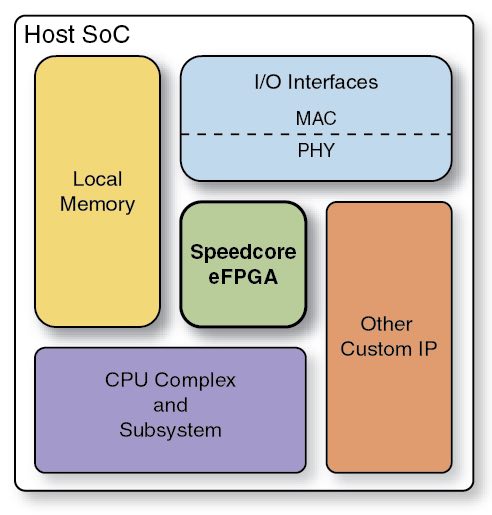
Once the benefits of using an embedded FPGA fabric are understood, the next question is about how timing closure is handled between the ASIC and the eFPGA blocks. First let’s look briefly at the advantages. By moving the eFPGA on to the SOC die, tons of I/O logic and the need for any package and board interconnect will vanish. Package and board routing create messy signal integrity and timing issues that require SerDes and bus protocols to tame. The added benefits also include reduced power – less logic to drive – and much lower latency. Instead of using a pair of SerDes, now the ASIC and eFPGA talk over direct wired signal nets.

While talking to Volkan Oktem, Achronix’s Senior Director of Product Applications, about the topic of timing closure with eFPGA I learned that there are two approaches for connecting the eFPGA to signals on the ASIC side. The easiest way is to use what they call “simple timing mode”, where there is a register on each net to help timing handoff at the eFPGA boundary. Of course, if you want to have the eFPGA output a signal off-chip, the SOC can include any necessary interfaces. But, the eFPGA can be thought of as just more logic – that just happens to be programmable.

In simple timing mode, the eFPGA and ASIC regions can be timed independently of each other. Constraints can be used in the eFPGA synthesis to ensure external timing meets spec. Then the ASIC just sees the eFPGA as a well-behaved block on the chip, like any other. For simulation, there is a gate level netlist with timing back annotation for the eFPGA so that top level timing can be verified.

If designers want to get rid of the extra clock cycle delay required by the intermediary registers, they can use the “advanced timing mode” which allows a direct connection from the ASIC logic to the input or outputs in the eFPGA. The catch is that the timing on these paths is now shared between the ASIC and the eFPGA. Achronix supplies a methodology that facilitates timing closure when using the advanced timing mode. First the user performs STA on the entire design, including the ASIC logic and the eFPGA logic. Next Achronix supplied scripts are used to extract the ASIC and eFPGA portions of all the nets that cross the boundary between the two parts of the design. Then these delays are passed as constraints to the ACE eFPGA tools so the eFPGA can be synthesized to meet timing. If there is more than one application for the eFPGA this process can be repeated for each.

After an iteration of the above process, designers can see if timing it met. If not, additional optimization or clock period adjustments can be made to close timing. While there is more effort required to use the advanced timing mode, it may well be worth it. Adding an eFPGA block to the floorplan otherwise is not much different than adding any other IP block. There are a few caveats, such as through routing is not allowed. So, placement of the eFPGA should take in to consideration the top level ASIC routing needs. There are no special supply or clock requirements.

An interesting side-note that came up in my conversation with Volkan was that for debug and test it is possible to program part of the eFPGA with special testers and debugging aids. This can help improve testability and visibility for the eFPGA and also the surrounding ASIC logic.

Volkan also pointed out that for some customers the goal is just to make a portion of an SOC programmable, adding for instance the flexibility being able to make post silicon logic changes. This affords the ability to refine and adapt functionality much later in the development process. However, he explained that sometimes their customer’s goal is to create special a purpose FPGA device, one that is tailor made for a specific application. This can have a number of advantages over off the shelf FPGA parts.

With a straightforward integration process, either with interface registers or through direct connection, the addition of programmability to an SOC design can be tremendously beneficial compared to off chip FPGAs or going without programmability altogether. Volkan has been working on developing new tools and documentation to make this process easy and efficient. There are resources on the Achronix website that go into much more detail and further explain clocking options and the timing closure process.


Timing Channel Attacks are Your Problem Too

Timing Channel Attacks are Your Problem Too
by Bernard Murphy on 08-07-2018 at 7:00 am

You’ve heard about Meltdown and Spectre and you know they’re really bad security bugs (in different ways). If you’ve dug deeper, you know that these problems are related to the speculative execution common in modern processors, and if you dug deeper still you may have learned that underlying both problems are exploits called timing side-channel attacks which depend on differences in timing between different operations, for example in retrieving data from a cache on a hit or miss. From there on for many of us, certainly for me, the details get a lot harder to follow.

But you probably thought (as I did) “this is a problem for the CPU guys, not my concern”. Bad news – you need to worry about this too. Timing channel exploits are not just for CPUs and caches. Timing exploits are possible through NoCs, in accelerators, between accelerators and their caches, pretty much anywhere an attacker might probe for hints to privileged information. We can’t just punt this to someone else; we need a deeper level of understanding.

So I talked to Jason Oberg, CEO of Tortuga, who has a PhD in timing channels; he managed to drag me through the basics. I say “drag” with feeling because just understanding the basics was hard; trying to reason about whether you have timing channel problems in a large design may earn you an extended stay in a sanitarium. They’re hard because this class of problem inherently spans multiple instructions and requires you to look at both software and hardware together. To see why, Jason shared a couple of the “easier” examples. These assume a victim process and an attacker process can run on the same system (under a VM OS for example).

First, think about a public-key cryptography system – could be in hardware or software. This depends on calculating a number to a power (the key) then taking the modulus of the result to some base. The most efficient standard way to do this uses a square-and-multiply algorithm, progressing over bits in the key. Square and multiply operations take different times and use of these operations differs for 0 and 1 bits in the key, therefore total time taken for the operation (if you have access to a sufficiently accurate clock) reveals the number of ‘1’ bits in the key. So start a timer, run the encryption, stop the timer and read the result. Since the key won’t change, repeat with multiple carefully-selected plain-text inputs, analyze the timing variations for these inputs and you can reconstruct the key one bit at a time.

The crypto-experts figured this out and one came up with a better algorithm called Montgomery’s ladder, which is immune to this kind of attack because it balances operation times for 0 and 1 bits. But then the experts found another way to force timing variations, through data retrieval times from the cache. Hang on to your hats – this is going to get complicated. One approach starts with something called a Prime and Probe attack. Before running the encryption test, the attacker primes the cache by filling with its own cache lines. Then the attacker times an encryption test, as before. Subsequently the attacker swaps back in and checks if any of the cache lines it preloaded have been evicted by the encryption. If they have, each such operation would have taken longer to execute in the encryption.

Now back to Montgomery’s ladder. This also steps through the key bitwise and performs different operations in each case depending on whether the bit is 0 or 1. But because of the Prime and Probe setup, now timing is sensitive to memory indexing from the ladder operation in the victim process and that indexing is still based on progressive bits in the key. From there you just continue to run analyses over multiple plain-text samples, analyzing the timing variations for these operations, from which you can ultimately extract the key.

Reminder – these are just examples; nothing about them is particularly restricted to CPUs, caches or encryption. Timing channel vulnerabilities can happen all over the place, as I mentioned earlier. And you can’t figure out where you might have such a problem without looking at hardware and software together. Formal and other standard security tools really can’t help. Even thinking about where you might have such problems can be difficult. You probably should talk to Tortuga who have a strong background in this domain and have built tools particularly around finding timing channel problems.


Cadence Update on AMS Design and Verification at #55DAC

Cadence Update on AMS Design and Verification at #55DAC
by Daniel Payne on 08-06-2018 at 12:00 pm

As a blogger in the EDA industry I get more invitations to meet with folks at DAC than I have time slots, so I have to be a bit selective in who I meet. When the folks at Cadence asked me to sit down and chat with Mladen Nizic I was intrigued because Mladen is so well-known in the AMS language area and he’s one of the authors of, The Mixed-Signal Methodology Guide: Advanced Methodology for AMS IP and SoC Design, Verification, and Implementation. You can buy this book at Amazon for just $115.00 and you’re sure to get a great ROI for the time spent reading it.


Prior to Cadence you find that Mladen worked at both Silvaco and Anacad, so he has a rich history in TCAD and circuit simulation tools.

Q: What are the trends with AMS simulation these days?

For AMS simulators we see that the performance always keep improving, from SPICE-level all the way up to digital. In my recent focus in AMS methodology, we are trying to leverage simulation to do better verification. Verification planning and managing your simulations for analog are now more important, because we need to be smart with simulation.

Model-based verification is becoming mainstream in Mixed-signal. Now with Real Number Modeling in Verilog and System Verilog designers are picking these languages. AMS modeling is a challenge, and it can be approached either top-down or bottom-up.

More engineers are becoming modeling specialists, as they know circuit design, CAD tools and verification approaches. They are asking themselves, what needs to be modeled?

Q: What are the challenges of modeling of AMS blocks?

To accurately model the characteristics of an analog block does require some circuit design understanding, so in most cases it takes a team to create a model, then compare the model against specs or other circuit results.

Q: Have AI or ML techniques been used much for AMS modeling?

ML may provide some help to automate the process of moving a transistor-level netlist up to a behavioral model.

Cadence has templates to help build models more quickly, and the designer needs to know how much detail and accuracy is really needed. It’s the classic benefits versus investment, so don’t over-model and don’t spend too much effort in creating models.

Q: Who on the team should be creating AMS models?

Well, forcing analog designers to do modeling may not work.

Analog designers are changing to adopt modeling in order to meet shorter time to market demands, and there is now more willingness to look at new methodologies.

Q: How should I go about learning AMS modeling?

There are Design Services for learning modeling, plus an IP team can deliver most AMS blocks requested. Training is also available, take a look at the standard courses from Cadence Education Services.

Q: What is happening on the language standards front?

We have both Verilog-AMS and SystemVerilog (getting Extensions to RNM) . Cadence is involved in standards committees and SystemVerilog AMS will become a standard in about 2020 and that process is under IEEE control.

Q: Is cloud-based EDA going to work this time?

In the cloud we see companies mixing and matching their simulation runs, both private and public clouds. Tasks that take the most time fit the cloud model quite well: library characterization, MC, validation or regression. All of the key apps are ready on the cloud today.

Related Blogs


Synopsys Offers First Single-Vendor Comprehensive Photonic IC Design Flow

Synopsys Offers First Single-Vendor Comprehensive Photonic IC Design Flow
by Daniel Nenni on 08-06-2018 at 7:00 am

Synopsys has a long history of being a thought leader and it’s not surprising to see the company jumping into the forefront of new technologies. For decades, I’ve been steeped in electronic IC design and it caught me by surprise to find that Synopsys had been quietly working on filling out their portfolio in the optical design solutions space. This first caught my attention with Synopsys’ 2014 acquisition of Brandenburg GmbH, who were known for their LucidShape product. LucidShape is used for design and simulation of automotive lighting systems. My assumption at the time was this was a move to help bolster Synopsys’ position in automotive markets.

What I didn’t realize was that Synopsys had already made two other acquisitions in the optical-space: Optical Research Associates (ORA) in 2010 and the RSoft Design Group (RSoft) in 2012. It turns out that Synopsys was already well on its way to building arguably the largest and most experienced optical design automation and services organization in the world. The ORA acquisition brought Synopsys decades of optical design experience (the company was originally founded in 1963), while the RSoft business, which released its first software package for the integrated optics industry in 1990, brought Synopsys into the realm of photonics and Photonic Integrated Circuits (PICs) with a full catalog of powerful optical system-level and device-level simulation tools.


Most recently, Synopsys acquired PhoeniX Software, a leading PIC and MEMS implementation tool provider. RSoft and PhoeniX also brought Synopsys decades of experience in photonic CAD and design, having their origins in the very early 1990’s.

In case you are wondering to what purpose Synopsys is doing this, I should note that the companies that now make up the Optical Solutions Group of Synopsys are already bringing in significant revenues. Strategically, this is just the beginning and it’s coming at just the right time. The IoT, 5G, big data, artificial intelligence, autonomous self-driving vehicles, and quantum computing are all on the cusp of exploding onto the market and they all have one thing in common: an insatiable need to be able to move and process huge amounts of data, further accelerating the need for optical data communication networks and data center infrastructure.

Therein lies an inflection point for Synopsys. Photonics (especially integrated photonics combined with integrated electronics) holds the promise of moving orders-of-magnitude more data at orders-of-magnitude faster speeds with — catch this — orders-of-magnitude less power! In less than a decade, Synopsys has brought in hundreds of person-years of optical experience and is marrying that experience with some of the best EDA tools in the industry.

With the PhoeniX acquisition, Synopsys has filled in an important technology gap and is now the first supplier to be able to offer a full front-to-back PIC design flow with all tools coming from one company. They can now address everything from system-level optical systems through fully integrated photonics on a chip, all from one company. No one else in the industry can offer this today. The obvious benefit to users is that you can expect the design flow to work well together and, if it doesn’t, there is no finger pointing back and forth between vendors. You have one company to hold accountable. On a more positive note, Synopsys is able to work all of the pieces to make for a better flow, which is important at the early stages of a technology when things are rapidly changing.

As a quick overview, consider the following PIC design flow from Synopsys:


Not only does Synopsys have the most complete photonics and optical solutions offering, but they also boast the most comprehensive PDK support for photonic foundries and package suppliers. Synopsys supports over 30 PDKs available on a variety of photonic platforms such as Indium Phosphide, Silicon, Silicon Nitride, Silicon Germanium, Polymers, etc. The tool flow also allows designers to add their own custom building blocks to any technology to take advantage of the best of both worlds (custom and pre-characterized PDK building blocks).

Consider also that photonic systems usually require some type of electronic control. Who better than Synopsys, with their strengths in EDA, IP, and software solutions, to combine these domains with photonics? New markets can take a while to sort themselves out. Photonics and how it combines with electronics will be no different, but with fast-growing markets like those already mentioned, and the technology Synopsys is bringing to bear, you can start to see a real powerhouse emerging for next-generation designs.
See also:

Synopsys Optical Solutions Group Home Page
Synopsys Driving the PIC Revolution Datasheet

A big thank you to my friend Mitch Heins of Synopsys for his contributions to this article.


Career Change Advice and how EDA Hiring has Changed

Career Change Advice and how EDA Hiring has Changed
by Mark Gilbert on 08-05-2018 at 7:00 am

I think most of us can attest that changing jobs is one of the most stressful decisions we make, as our careers progress. Making a job change is rarely an easy decision, though admittedly, so wonderful when it accomplishes your career and life goals. Having the right, well thought out expectations is the best way to ensure success, and not waste your or anyone else’s time. Here is the best way to approach a career change…

First, think of where you are now… is this position, the role you want, for the next several years? Is the team you work with, a team you enjoy working with? Do they make you feel good, comfortable about coming to work every day? Does the company have a product that interests you and are they doing well? Does their product work, scale and have longevity in the market? Do they treat their employees well? Are you looking for something different? What might that difference look like? It is these questions and more that should always be considered before making the decision to start looking or interviewing.

Once you have decided to start exploring, or perhaps follow up on a position that you just learned of, either through a friend or recruiter, make sure that you are prepared for all of the next steps. While your technical abilities will certainly make or break the outcome, there are other key preparations that can help you maximize your success through the process. One key ingredient to add to the formula, is the use of a highly specialized INDUSTRY recruiter. This one key ingredient can increase your chances of a great and lasting outcome. To start, a good recruiter will help you examine your reasons for wanting to make a career move. The right recruiter can prepare you, giving you insights into the process, as well as the dos and don’ts, and timing of what to say when, which should all help to ensure that you present yourself, in the best light.

A successful experienced recruiter will walk you through the interviewing process, using their own proven formula to prepare you each step of the way, further ensuring your chances of a successful outcome. Proper interviewing techniques is key to a good outcome, regardless of how good you are technically. More importantly, that recruiter, if they are good and have relationships with the hiring company, should do all the post-interview follow ups, on both sides, so that the process keeps moving forward.

Bottom line: getting hired in today’s job market is no easy task. Companies are more particular in who they hire, than ever before. The good news is, there are far fewer candidates looking so the pool is smaller, making your chances a little better. Companies want people that can make an immediate contribution. When applying, save yourself time by applying to things within your wheelhouse, and perhaps go out a few spokes. In the tech world we all play in, it is all about innovation and new approaches to problem solving. Know your strengths and play to them. Make sure your resume has all the key ingredients to excite and interest the person reading it. If your resume does not catch their eye, regardless of how good you are, you have no chance of getting the call.

In my next blog, I will cover some more good reasons for considering a career change as well as good tips for structuring a strong resume.


An update on the Design Productivity Gap

An update on the Design Productivity Gap
by Tom Dillinger on 08-03-2018 at 12:00 pm

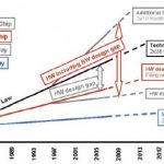
Over a decade ago, a group of semiconductor industry experts published a landmark paper as part of the periodic updates to the International Technology Roadmap for Semiconductors, or ITRS for short (link). The ITRS identified a critical design productivity gap. The circuit capacity afforded by the Moore’s Law pace of technology advancement was growing faster than the capabilities of EDA tools and flows to support the associated design complexity. The figure below captures the ITRS projections at that time.

Note that the ITRS experts recognized the increasing influence of design IP (and its reuse) to help mitigate the gap. Nevertheless, this ITRS report served as a ‘call to action’ for the EDA industry to address methods to improve design productivity.

Fast-forwarding a decade, how has the landscape changed? Moore’s Law has continued to enable tremendous growth in circuit density, a testament to the expertise and ingenuity of fabrication engineers and equipment manufacturers. Note that this process technology evolution has been achieved without a reduction in reticle size, truly an amazing achievement.

Many EDA tools have been re-architected (and design models optimized) in support of multi-threaded (and in some cases, distributed) computation for very large datasets.

EDA platforms have been introduced, integrating analysis algorithms into implementation flows to improve optimization decisions, and thus overall design closure schedules. In support of these timing, noise, and power optimizations, the design model (and cell library model) complexity has grown – this adds to the stress on dataset size.

I was curious to know, “How has the industry progressed in closing the productivity gap? What are the areas where the gap remains?”

At the recent DAC55 in San Francisco, Cadence assembled a panel of industry and EDA experts to address the topic:

“Monster Chips – Scaling Digital Design Into the Next Decade”

The panel participants were:


  • Chuck Alpert, Senior S/W Group Director for Genus Synthesis, Cadence
  • Anthony Hill, Fellow and Director for Processor Technology, Texas Instruments
  • Antony Sebastine, Principal Engineer with the Systems Group, ARM
  • Anand Sethuraman, Senior Director, ASIC Products, Broadcom
  • Patrick Sproule, Director of Hardware, P&R Methodology, Nvidia Corp.

Here are some of the insights the panel shared – both acknowledging the strides made in addressing the design productivity gap and highlighting remaining challenges.

Advances
“The growing use of (multiple instances of) hard IP has required significant focus on macro placement. Automated macro placement in design blocks has improved significantly – routing congestion is reduced.”

“DRC throughput – especially approaching tapeout – is always time-critical. The (distributed) physical design verification tools have kept runtimes in check.”

“The ECO-based flows to close on timing issues have improved substantially.”

“The signal buffering and advanced layer selection algorithms in GigaOpt provide better physical implementations—of course, pre-route to post-route correlation is always a challenge.”

Challenges

“Design implementation capacity must be improved. The Quality of Results (QoR) for blocks greater than 2 million instances tends to degrade substantially.”


“Agreed. We are constrained to block sizes of 1M-3M instances to achieve suitable turnaround time and QoR. The design partitioning overhead in floorplanning and constraint management is cumbersome. We need to be able to support block sizes of 20M-30M instances to keep pace with the technology.”


“We are utilizing physical design servers with 40 processors and 768GB to 1TB memory, but the (multi-threaded) jobs are still limited in throughput.”

“A flow of increasing importance is the calculation of dynamic P/G grid IR voltage drop, and the impact on timing margins. The tools need to have the capacity to support activity-based analysis on very large networks.”

Expanding upon the last comment, the significance of dynamic voltage drop (DvD) on design closure was a common theme throughout the DAC conference, both in technical presentations and the EDA vendor exhibit floor. Current SoC designs commonly incorporate several features that increase the sensitivity of timing analysis calculations with DvD-based characteristics:


  • dynamic operation voltage domain optimization (DVFS)
  • non-linear cell and interconnect delay dependence upon (reduced) P/G voltages
  • (aggressive) library cell track allocation to the P/G rails

At advanced process nodes with aggressive voltage domain and power optimizations, static IR drop P/G analysis (with fixed cell characterization margins) will be increasingly problematic.

Summary

Chuck A. from Cadence offered a unique perspective to the comments from the other panel members. “Cadence wants to partner with design teams working on difficult blocks. We evaluate our implementation platform QoR on our internal testcases, but would benefit from a closer collaboration, to better understand the issues presented by specific designs.”

The takeaways from the discussion that I noted are:

Several EDA tool areas have made significant improvements in designer productivity and support larger dataset sizes – e.g., analysis-driven optimization algorithms, multi-threaded and distributed algorithms.

Nevertheless, designers are continuing to face the productivity gap identified a decade ago – support for block sizes of 20M-30M instances is required to keep pace with Moore’s Law. Specifically, physical design implementation flows require (academic and industry) research focus to be able to accommodate larger block sizes. Collaborative partnerships between (leading-edge) design teams and flow developers are required.

Patrick S. from TI reminded the audience that there will be an increasing demand to integrate reliability-based analysis algorithms into implementation platforms – e.g., EM, aging mechanisms. The goal would be to exit implementation and be ready for reliability sign-offmuch as EDA platforms strive for timing/noise signoff quality.

Alas, the EDA productivity gap is still present – a factor of 10X improvement in throughput is needed.

At DAC, I bumped into a professor colleague who lamented that EDA academic research funding was drying up, as there is a general perception that “all big EDA problems have been adequately addressed… the money is going to proposals associated with machine learning and AI.”In actuality, the challenges of efficient design data modeling, development of (tightly-correlated) optimization algorithms, and opportunities for improved (distributed) processing are more important than ever.

I guess you could consider this to be a 2018 version of the ITRS call to action.

-chipguy


Speak N Spell

Speak N Spell
by Daniel Nenni on 08-03-2018 at 7:00 am

This is the ninth in the series of “20 Questions with Wally Rhines”

Success has many authors and the Speak & Spell product from Texas Instruments generated lots of write-ups to demonstrate this. For most of the semiconductor industry, results of innovation were not apparent to the masses but, for the consumer electronics that emerged in the 1970s, the innovations were visible, exciting and fun. My job in the Consumer Products Group (CPG) was Engineering Manager with responsibility for the design and development of all the chips and plastic cases used in TI’s fledgling consumer business. In early 1977, almost all of CPG was moved from Dallas to Lubbock. From then on, we performed the logic design for our chips in Lubbock while the physical layout was done in Houston under the direction of K. Bala, an energetic, driving manager who was perfect for the task of juggling dozens of complex designs while competing for resources with TI’s traditional semiconductor business.


From left to right, Gene Frantz, Richard Wiggins, Paul Breedlove and Larry Brantingham

Paul Breedlove was in charge of product development for the “Consumer Calculator Division” which was managed by Jim Clardy (later CEO of Harris Semiconductor and then co-founder and CEO of Crystal Semiconductor (which ultimately became Cirrus Logic). Jim and Paul had a miserable job. Japanese manufacturers like Casio, Sharp, Toshiba and many more could design and manufacture great “four function” (add, subtract, multiply and divide) calculators for less than TI could. By late 1977, TI was reselling Toshiba four function calculators with a TI label because they were more profitable than our own. Paul kept searching for a differentiating alternative and he found it by attending one of the monthly “Research Reviews” that were held in the Central Research Laboratories (CRL) and open to TI employees from other parts of the company. At this particular review, Richard Wiggins presented the technology he was developing for speech synthesis. He was approaching a capability of producing understandable speech at a data rate of only 1000 bits per second. Paul was fascinated. Why not develop a product that took advantage of speech to differentiate, or augment, traditional consumer electronic products? Paul was helped along by the analogy of one of the few really profitable, successful consumer calculators called “The Little Professor” which was an arithmetic learning aid for children. Every year we expected revenue for the Little Professor to decline but it seemed to have a life of its own. We were beginning to realize that parents will pay any price to give their children an advantage in the education system.

As an experiment in innovation, TI had recently established a funding mechanism called the “Idea Program” where any employee could propose an idea for a product or technology and, if approved, receive $25,000 of funding to demonstrate feasibility. Paul submitted an Idea Program proposal (probably because the Consumer Calculator Department was really squeezed for funding) and Ralph Dosher, the CPG Controller, approved it. That’s when I became involved. Paul needed someone to figure out how to design chips that could be used in the product. Larry Brantingham worked in the Logic Design Branch of the Engineering Department I ran and he became the obvious choice.

Speech synthesis chips were under development at National Semiconductor and other companies but success was very limited because the current state of the art N-Channel MOS, or NMOS, technology was just too slow to achieve the needed performance for this computationally intense application. What is so remarkable about Speak ‘N Spell is that Larry didn’t use the higher performance NMOS technology but instead used the much slower P-Channel MOS, or PMOS. Why, you might ask? Very simple. Larry didn’t know how to design with NMOS. In addition, CPG was in a continuous battle with the Semiconductor Group over pricing of chips and Morris Chang, Semiconductor Group VP, became tired of all the arguments and settled the dispute by offering CPG a flat $25 price per two-inch wafer of PMOS, which was a five photomask process at that time. If Larry had learned how to design with NMOS, the program would have failed because the cost of NMOS wafers would have been too high. While the artificially subsidized price for PMOS made the cost feasible, the performance seemed much to slow.

Larry went to work with Richard Wiggins designing a pipelined multiplier in PMOS. Responsibility for the product was moved from Consumer Calculators to Specialty Products which was run by Kirk Pond (later CEO of Fairchild Semiconductor) because, although Consumer Calculators were struggling, the Specialty Products Divisions was struggling even more to find new product possibilities. Gene Frantz was enamored with the product and quickly became product manager, tasked with all the issues of choosing product features, name, marketing, etc. as well as managing the overall product development (Figure One)

Even more ridiculous than designing a pipelined multiplier for the synthesis chip was the task of designing read-only memory (ROM) chips big enough to store the pre-recorded speech vocabulary. When I presented the proposed chip design program to the TI Corporate Development Committee, Dean Toombs, head of R&D for the Semiconductor Group argued that the engineers in CPG had gone crazy. Semiconductor Group was struggling to produce the NMOS 2716 ROM at very low yields. If they couldn’t produce a 16K ROM, how could CPG design a 128K bit one? What Dean overlooked, however, was the fact that the TMS 2716 needed an access time of 450 nanoseconds while our speech chips could be dramatically slower. PMOS was also an older, more mature technology and was easier to produce than the highly advanced NMOS. So we received approval to go ahead and received corporate funding to develop a four-chip system with a synthesizer, controller and two 128K bit ROMs (Figure Two).

As the actual die size increased beyond the original estimates, the estimated cost of the chips increased. At one point, Kirk Pond threatened to kill the whole program because it was well known that $40 was a critical point for consumer products where both spouses had to approve the purchase. By the time Speak ‘N Spell was introduced, the suggested retail price was $60 and it sold so well that we quickly raised it to $65. Like the Little Professor, parents just couldn’t resist the purchase of an educational aid that would help their children spell, even though the synthesized speech sounded more like a robot than a human. Shortly after the introduction, we were invited to show the product on the Today Show, the most popular TV news program of the day. Charley Clough, our highly articulate and lovable head of Semiconductor Group sales walked Jane Pauley through the steps of using Speak ‘N Spell while Gene Frantz was behind stage with backup units since the reliability of our early production units wasn’t very good.

Speak & Spell took the world by storm and became a great story of corporate innovation. Not long after the introduction, I moved to Houston and took over the Microprocessor Division where we developed the TMS 320 single chip digital signal processor, or DSP. Although I was the only one who worked on both programs, there was at least a remote connection to the theme of digital signal processing in TI’s speech synthesis success. And DSP became the cornerstone of TI’s next wave of growth.

The 20 Questions with Wally Rhines Series


Netspeed and NSITEXE talk about automotive design trends at 55DAC

Netspeed and NSITEXE talk about automotive design trends at 55DAC
by Tom Simon on 08-02-2018 at 12:00 pm

DAC is where both sides of the design equation come together for discussion and learning. This is what makes attending DAC discussion panels so interesting; you are going to hear from providers of tools, methodologies and IP as well as those who need to use them to deliver working solutions. There are few places where the interplay between design activity and the tools necessary to accomplish it are more important than in the rapidly changing area of automotive electronics. For decades cars basically had coils and capacitors. Then came radios. But in just the last few years the complexity of automotive electronics has leapt to the upper end of the spectrum.

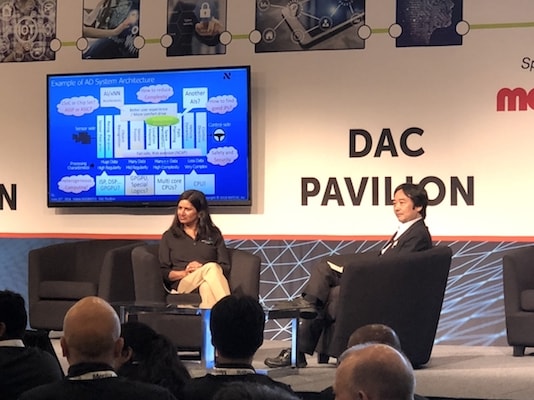
As usual power efficiency and performance are essential, however, in addition, safety has become a top line requirement. So, it was interesting to see the “fireside chat” hosted at DAC by Netspeed on the topic of “Design for Safety and Reliability – ADAS and Autonomous Vehicle SoCs”. Netspeed CEO Sundari Mitra interviewed Hideki Sugimoto from NSITEXE, the Japan based supplier of SOC IP for automotive autonomous driving systems.

Sundari started the session off by pointing out that the rapid growth in automotive semiconductors is fueled largely by the development of ADAS and autonomous driving systems. She asked what are the major trends and what are the needs and challenges that are created by them. Sugimoto replied that he has seen three major trends.

The top OEMs and Tier One vendors have very specific performance, safety and power goals. It used to be that ASSPs worked well enough, but off the shelf parts, even when tailored for specific markets, are not good enough anymore. So now all the players are involved in some way with ASIC development.

Now, within ASIC design, there has been a need for a shift from hand tuning each part of a chip to achieve performance goals. This was fine when the SOCs has fewer blocks, but now the better way to meet requirements is to start at the top level and map out requirements thoroughly. The requirements need to be specified in terms of end use-case performance or power goals.

The last trend is the move towards heterogeneous computing. The SOCs needed for ADAS or autonomous vehicles are extremely complex and their performance cannot be improved just by adding more CPUs or GPUs. The right way to carefully match up the right mix of the above and also add special purpose processors and accelerators for things like machine learning. Sugimoto’s company NSITEXE has a strong track record in this area, so these observations are borne out of direct experience.

Sundari followed with a question on the specifics of a requirements driven approach to putting chips together. Sugimoto cited the need to really look at the system level and not just focus on the chip itself at the outset.

The main performance factors are throughput, latency and end to end QoS. At the same time, all of this needs to be done without compromising safety. Sugimoto pointed out that you can’t bolt on the safety elements later and you also cannot achieve your performance goals without considering the safety requirements early in the process.

Sugimoto feels that there are three must have capabilities in an architectural design solution for automotive chips. They are (a) handling heterogeneous compute elements and coherency (b) delivering high QoS across all types of workloads and (c) ASIL-D and ISO 26262 certification. Every one of these affects safety security and reliability. The maximum amount of data must be extracted from the sensors. This means higher bandwidth and more processing. Sugimoto emphasized heterogeneous computing is really the only solution. However, this makes the chip architecture more complex. Sugimoto sees Network on Chip as a critical tool for managing this complexity and still being able to achieve design goals. NoCs can help provide determinism in these systems through the addition of memory coherency and QoS, for instance. Naturally the NoC will also have to comply with ISO 26262.

Looking at the conversation it is clear that automotive is now the killer app for advanced SOC design tools. This is where the greatest challenges are. The combination of the unique environmental, power, safety and functional factors make this a very interesting prospect. I have been covering Netspeed for some time now and can see how they are looking at the automotive market as a space where their NoC technology can make a big difference. Their website has more information on designing SOCs for automotive applications. It’s worth taking a look.


KLAC gets an EUV Kicker

KLAC gets an EUV Kicker
by Robert Maire on 08-02-2018 at 7:00 am

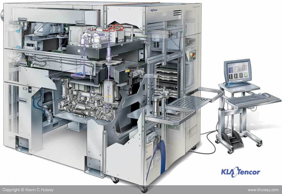
KLAC put up a great quarter coming in at revenues of $1.07B and EPS of $2.22. Guidance is for $1.03B to $1.1B with EPS of $2 to $2.32. Both reported and guided were at the high end of the range and above consensus. We had suggested in our preview notes that KLAC would be the least impacted of the big three (AMAT, LRCX & KLAC) semi equipment companies by the current memory volatility.

That has turned out to be the case as KLAC will likely see less than a 10% slow down in shipments and essentially zero impact on revenue and earnings versus the 25% drop in revenues expected by Lam along with an EPS drop below the low end of the range. We still predict that AMAT will fall somewhere between KLAC’s zero revenue impact and Lam’s 25% fall off probably coming in at a 10%-15% drop in revenues.

KLAC is obviously much less exposed to the more volatile memory sector and thus didn’t see as much of the sharp increase or sharp decline and has historically been a more consistent performer. KLAC reported record high shipments, revenues and EPS in the quarter and continues its juggernaut like roll. The company also was more forceful about its view of the December quarter calling for a “sharp snap back” rather than the more nebulous “positive trajectory” offered up by Lam.

We expect memory capex spending to continue to be quickly modulated by pricing and demand trends with either long or short term volatility and cyclicality as the industry keeps one foot on the accelerator and the other on the brakes. Having a very good balance and diversification that KLAC has will provide more consistent longer term performance and likely deserves a higher multiple,as compared to others, for the reduced volatility. We also expect ASML to have a similar performance to KLAC with minimal memory impact given its steadier long term history.

Market positioning remains very strong as the industry needs metrology and yield management tools to get the process fine tuned before they go out and buy the process tools that vary more with demand and output.

An EUV kicker
The transition to EUV is anything but easy. Aside from ASML who is the obvious beneficiary of the transition we think that KLAC could see if not as much benefit but perhaps even more especially in the current early stages of the transition where the problems are the greatest. ASML’s EUV revenue also replaces its DUV revenue so there is a bit of an offset which KLAC does not see.

This compares to dep and etch players who have nothing but downside as the number of overall dep and etch steps will without doubt be lower under EUV processes as compared to DUV processes. We think that KLA is another way to play the EUV transition for those who do not want to put all their eggs in ASML’s basket.

Financials are best in the industry
With industry leading gross and operating margins coupled with ATM machine like cash generation, whats not to like. The financials underscore the pricing power of being the market leader in the process control part fo the industry.

More diversification coming
The pending Orbotech acquisition will bring even more diversification to KLA’s model and further insulate it from volatile single end markets. We think this addition of SAM to an already strong base will further strengthen the story.

China exposure helps KLA
KLA is likely seeing more benefit than others from the growing China market as a lot of money is being spent in China by chip companies trying to come up to speed and perfect processes. Something that is almost impossible to be done without KLA tools. While China has more alternative sources for process tools there are really no alternatives to KLA tools which they have to keep buying in quantity.

The Stock
We continue to favor KLAC over both LRCX and AMAT. Not only are the financials way better but the risk is much lower as demonstrated by KLAC’s performance this quarter which barely registered a blip at KLAC but is causing heartburn elsewhere. The company well deserves a higher multiple for this more consistent performance along with better financials and diversity.

This more consistent performance may not be as flashy on the way up but avoids the near term pain and stock gyrations on the way down. In general we feel a lot safer in KLAC stock right now and probably for a couple of quarters until we get better visibility on memory. The near term factors are most aligned with KLAC right now and their stock should be a better performer.


Accelerating the PCB Design-Analysis Optimization Loop

Accelerating the PCB Design-Analysis Optimization Loop
by Tom Dillinger on 08-01-2018 at 12:00 pm

With the increasing complexity and diversity of the mechanical constraints and electrical requirements in electronic product development, printed circuit board designers are faced with a number of difficult challenges:

  • generating accurate (S-parameter) simulation models for critical interface elements of the design – i.e., connectors sockets, (twisted-pair) cables
  • developing comprehensive simulation/analysis models for entire packaging solutions – e.g., rigid-flex board topologies
  • accelerating the design optimization-analysis feedback loop

Given the aggressive schedules allocated to PCB development, typically dependent upon completion of key IP/SoC/module design milestones, the last challenge above is especially critical. The evaluation of interface compliance measures – e.g., timing/voltage margins, eye diagrams, bit error rate estimates – may necessitate board design updates, which then need to be re-analyzed. Minimizing the time and engineering resource (and the risk of an error) to close on implementation-extraction-analysis iterations is crucial.

I had the opportunity to chat with Brad Griffin, Product Manager Group Director at Cadence, about these challenges, and some of the features incorporated in the recent Sigrity 2018 release that will significantly alleviate them.

Brad indicated, “Bridging the gap between the mechanical model of interface components and the corresponding electrical model for power integrity and signal integrity simulation is a key addition to this latest release. The Sigrity 3D Workbench takes the physical Allegro board model as input, and applies full-wave field solver technology to derive the S-parameter model for simulation.”

The examples below illustrate the mechanical model of board-mount connector pins, which would be presented to 3D Workbench for S-parameter model generation. (The “breakout” of the board trace is included in the full-wave field solver input, to the point where a 2D hybrid solver analysis of the PCB trace can be applied.) The physical models of cables, connectors, and sockets are also analyzed by 3D Workbench.

An illustration of how 3D Workbench is used in a larger flow is depicted below. Brad said,“This 3D Workbench capability is a new component of existing flows, such as the Serial Link Compliance validation solution shown in the figure.”

Brad continued, “Our internal IP group develops high-speed SerDes and parallel interface (DDRx) offerings, verified to the compliance measurements associated with industry standards. The Allegro and Sigrity teams collaborated closely with the IP group on the functionality and testing of 3D Workbench and the Sigrity 2018 release.”

With regards to the growing utilization of rigid-flex technology, Brad noted, “There is a comprehensive connection between the rigid-flex design and analysis flows. Allegro is integrated with the extraction and simulation features of Sigrity PI/SI. Again, a mix of full-wave models(from 3D Workbench)and 2D hybrid solver models can be extracted, stitched, and simulated.”

The figure below illustrates a rigid-flex design with the corresponding visualization of the Sigrity PowerDC results. (Note the power distribution in the flex cable to the mezzanine card on the right results in significant losses.)

Speaking of the integration between Allegro and Sigrity, Brad was excited about the productivity gains this enables. SI/PI engineers can make their design changes in the Sigrity environment, re-extract and simulate – e.g., a specific via array pattern optimized to meet loss targets. Brad highlighted, “A key feature in this release is that updates made in the Sigrity platform are directly incorporated into the Allegro model, without the need to re-draw.”

The handoff of “markup” requests from the SI engineer to the physical design team is eliminated, improving the rate of design closure (and reducing errors) in the final optimization phase before release for PCB fabrication.

Future Challenges

I asked Brad about upcoming challenges for PCB (and rigid-flex) designers.

“I’ll point out two of the areas we’re working on.”, Brad said. “In the future, support will be provided to work with encrypted mechanical component models, for improved security of the component vendor’s intellectual property.”

“And, with the growing complexity of board designs, combined with the higher datarate defined for future interface IP standards, full wave model accuracy(out to multiple harmonics of the fundamental)will be required for a larger set of models. Full-wave mesh topologies will be denser, requiring greater compute resources. The methodology leveraging both full-wave and hybrid solvers for extraction and simulation will be distributed across multiple machines.”

The 3D model generation capabilities, the support for full system model PI/SI analysis with the combination of solvers (including intricate rigid-flex topologies), and the focus on improving the PCB design-analysis optimization loop are all part of the enhancements in the recent Sigrity 2018 release (link).

-chipguy