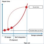
Banner Electrical Verification The invisible bottleneck in IC design updated 1

Webinar: Achieve High-performance and High-throughput with Intel based FPGA Prototyping

Webinar: Achieve High-performance and High-throughput with Intel based FPGA Prototyping
by Daniel Nenni on 03-19-2018 at 12:00 pm

FPGAs have been used for ASIC prototyping since the beginning of FPGAs (1980s) allowing hardware and software designers to work in harmony developing, testing, and optimizing their products. We covered the history of FPGAs in Chapter 3 of our book “Fabless: The Transformation of the Semiconductor Industry”, which includes a brief history of Xilinx. Of course ASIC design is much more complex now with exploding gate counts and a dizzying array of commercial IP and interfaces which brings us to today’s FPGA based prototyping systems.

“Designers using Intel FPGAs can now reap the benefits of FPGA prototyping with our A10 Single Prodigy Logic Module,” commented Toshio Nakama, CEO of S2C. “The new and unique sleek, metal enclosure that our A10 system comes in provides much needed flexibility, durability and portability that designers seek. Users, will of course, be able to take advantage of the full set of our leading Prodigy Complete Prototyping Platform components including Player Pro and Multi-Debug Module for advanced partitioning and debug.”

Webinar: Achieve High-performance & High-throughput with Intel based FPGA Prototyping

S2C Inc. has been successfully delivering rapid SoC prototyping solutions since 2003 with more than 200 customers worldwide. S2C has been on SemiWiki for two plus years with 30 blogs that have gathered more than 125,000 views. We also published a very popular free ebook “ PROTOTYPICAL – The Emergence of FPGA Prototyping for SoC Design”, so we know prototyping, absolutely.

I spent some time at the S2C HQ in San Jose (across from my favorite Starbucks) this week and actually got my hands on one of the new S2C Desktop Prototyping Systems and was quite impressed. My first question to S2C VP of Engineering Richard Chang was why would someone choose this new altera based system over an existing Xilinx system: Vendor bias plays a significant role (some people prefer Altera over Xilinx), others feel Altera is a better performing FPGA, but on this new product the desktop packaging is the big WOW factor. Here is a quick video I pulled from the S2C website:


This self contained prototyping system can be expanded from one FPGA to dual and quad FPGAs. Self contained so you can easily test your hardware/software design in a real world environment such as automotive or on the shop floor with an industrial IoT application. This truly is engineering driven packaging with an easy attachment for the dozens of daughter cards and interfaces available from S2C.

The base system starts at $10,000 and goes up from there. If you are ready to prototype and have end-of-year budget you can start HERE and get a quick quote, simple as that.

Webinar: Achieve High-performance & High-throughput with Intel based FPGA Prototyping

About S2C
S2C Inc. is a worldwide leader of FPGA prototyping solutions for today’s innovative designs. S2C was founded in San Jose, California in 2003 by a group of Silicon Valley veterans with extensive knowledge in ASIC emulation, FPGA prototyping, and SoC validation technologies. The Company has been successfully delivering rapid SoC prototyping solutions since its inception. S2C provides:

  • Rapid FPGA-based prototyping hardware and automation software
  • Prototype Ready™ IP, interfaces and platforms
  • System-level design verification and acceleration tools

With over 200 customers and more than 800 systems installed, S2C’s focus is on SoC/ASIC development to reduce the SoC design cycle. Its highly qualified engineering team and customer-centric sales force understands our users’ SoC development needs. S2C systems have been deployed by leaders in consumer electronics, communications, computing, image processing, data storage, research, defense, education, automotive, medical, design services, and silicon IP. S2C is headquartered in San Jose, Calif., with offices and distributors around the globe including the U.K., Israel, China, Taiwan, Korea and Japan.

Currently the US headquarters office is focusing on technology research, strategic alliances, sales and marketing for North America and Europe. The Shanghai office focuses on product development, with the Hsinchu office serving as the manufacturing center.


Don’t believe the hype about AI in business

Don’t believe the hype about AI in business
by Vivek Wadhwa on 03-18-2018 at 7:00 am

To borrow a punch line from Duke professor Dan Ariely, artificial intelligence is like teenage sex: “Everyone talks about it, nobody really knows how to do it, everyone thinks everyone else is doing it, so everyone claims they are doing it.” Even though AI systems can now learn a game and beat champions within hours, they are hard to apply to business applications.

M.I.T. Sloan Management Review and Boston Consulting Group surveyed 3,000 business executives and found that while 85 percent of them believed AI would provide their companies with a competitive advantage, only one in 20 had “extensively” incorporated it into their offerings or processes. The challenge is that implementing AI isn’t as easy as installing software. It requires expertise, vision, and information that isn’t easily accessible.

When you look at well known applications of AI like Google’s AlphaGo Zero, you get the impression it’s like magic: AI learned the world’s most difficult board game in just three days and beat champions. Meanwhile, Nvidia’s AI can generate photorealistic images of people who look like celebrities just by looking at pictures of real ones.

AlphaGo and Nvidia used a technology called generative adversarial networks, which pits two AI systems against each another to allow them to learn from each other. The trick was that before the networks battled each other, they received a lot of coaching. And, more importantly, their problems and outcomes were well defined.

Most business problems can’t be turned into a game, however; you have more than two players and no clear rules. The outcomes of business decisions are rarely a clear win or loss, and there are far too many variables. So it’s a lot more difficult for businesses to implement AI than it seems.

Today’s AI systems do their best to emulate the functioning of the human brain’s neural networks, but they do this in a very limited way. They use a technique called deep learning, which adjusts the relationships of computer instructions designed to behave like neurons. To put it simply, you tell an AI exactly what you want it to learn and provide it with clearly labelled examples, and it analyzes the patterns in those data and stores them for future application. The accuracy of its patterns depends on data, so the more examples you give it, the more useful it becomes.

Herein lies a problem: An AI is only as good as the data it receives. And it is able to interpret that data only within the narrow confines of the supplied context. It doesn’t “understand” what it has analyzed, so it is unable to apply its analysis to scenarios in other contexts. And it can’t distinguish causation from correlation. AI is more like an Excel spreadsheet on steroids than a thinker.

The bigger difficulty in working with this form of AI is that what it has learned remains a mystery — a set of indefinable responses to data. Once a neural network is trained, not even its designer knows exactly how it is doing what it does. As New York University professor Gary Marcus explains, deep learning systems have millions or even billions of parameters, identifiable to their developers only in terms of their geography within a complex neural network. They are a “black box,” researchers say.

Speaking about the new developments in AlphaGo, Google / DeepMind CEO Demis Hassabis reportedly said, “It doesn’t play like a human, and it doesn’t play like a program. It plays in a third, almost alien, way.”

Businesses can’t afford to have their systems making alien decisions. They face regulatory requirements and reputational concerns and must be able to understand, explain, and demonstrate the logic behind every decision they make.

For AI to be more valuable, it needs to be able to look at the big picture and include many more sources of information than the computer systems it is replacing. Amazon is one of the few companies that has already understood and implemented AI effectively to optimize practically every part of its operations from inventory management and warehouse operation to running data centers.

In inventory management, for example, purchasing decisions are traditionally made by experienced individuals, called buyers, department by department. Their systems show them inventory levels by store, and they use their experience and instincts to place orders. Amazon’s AI consolidates data from all departments to see the larger trends — and relate them to socioeconomic data, customer-service inquiries, satellite images of competitors’ parking lots, predictions from The Weather Company, and other factors. Other retailers are doing some of these things, but none as effectively as Amazon.

This type of approach is also the basis of Echo and Alexa, Amazon’s voice-based home appliances. According to Wired, by bringing all of its development teams together and making machine learning a corporate focus, Amazon is solving a problem many companies have: disconnected islands of data. Corporate data are usually stored in disjointed datasets in different computer systems. Even when a company has all the data needed for machine learning, they usually aren’t labelled, up-to-date, or organized in a usable manner. The challenge is to create a grand vision for how to put these datasets together and use them in new ways, as Amazon has done.

AI is advancing rapidly and will surely make it easier to clean up and integrate data. But business leaders will still need to understand what it really does and create a vision for its use. That is when they will see the big benefits.

For more, you can read my book Driver in the Driverless Car


Leading Edge Logic Landscape 2018

Leading Edge Logic Landscape 2018
by Scotten Jones on 03-16-2018 at 2:00 pm

The most viewed blogs I write for SemiWiki are consistently blogs comparing the four leading edge logic producers, GLOBALFOUNDRIES (GF), Intel, Samsung (SS) and TSMC. Since the last time I compared the leading edge new data has become available and several new processes have been introduced. In this blog I will update the current status.
Continue reading “Leading Edge Logic Landscape 2018”


Self-Driving Car Catch-22 and the Road to 5G

Self-Driving Car Catch-22 and the Road to 5G
by Roger C. Lanctot on 03-16-2018 at 12:00 pm

In the novel “Catch-22” from which the eponymous 1970 movie was made we learn of a fictional bureaucratic means by which the U.S. Air Force was able to keep bomber pilots (who might be going crazy) from successfully requesting a release from flying missions based on a medical evaluation. The rationale behind this supposed “catch” was that a pilot would be demonstrating his own sanity by asking to be relieved of this task.

In a similar way, European transport authorities seeking to foster autonomous vehicle development are grappling with longstanding transportation regulations that require the presence of a driver and the ability of the driver to take control of the vehicle. The regulations in question include parts of the Vienna Convention, the Geneva Convention and the UNECE’s WP.29.

Regulators throughout Europe are trying to thread this needle by allowing for the existence of automatic pilot systems but requiring the presence of a driver and the means for that driver to retake control of the vehicle. It is actually somewhat surprising that the EU has taken so long to address this question of driver presence and control because even mandated stability control systems represent precursors of driving automation but never triggered concern for changing the regulations.

The Catch-22 for vehicle autonomy arises as countries, such as Finland, introduce legislation allowing for robotic vehicles with remote control, meaning the vehicle must have a driver but the driver need not be present in the vehicle. One might say, in a twist on the Catch 22 concept, that you’d be crazy to deploy autonomous vehicles without remote control – but you’d be equally crazy to try to control robotic vehicles remotely.

Crazy though it sounds, this is precisely the scenario for which European autonomous vehicle contenders are preparing and which is likely to influence the process of modifying the extant regulations.

We already have some experience of this remote control scenario in the form of the infamous hack of an FCA Jeep two years ago by “ethical” hackers Chris Valasek and Charlie Miller, both of whom now reportedly work for General Motors. Phantom Auto is touting this capability as a core value proposition for vehicle autonomy. And Nissan has indicated its plans to enable remote control of its self-driving vehicles.

It is a very real prospect and reveals the shortcomings of the current regulator regime and the limitations of regulators. There are two major challenges facing the transportation industry: autonomous driving and cybersecurity threats.

In both cases, the process of vehicle certification for roadworthiness is subverted by the inability of regulators to certify that vehicles are secure or to determine, with any degree of certainty, that an autonomous vehicle will function safely in all circumstances. But politicians abhor a regulatory vacuum so the U.S. Congress has passed the Self Drive Act – a piece of legislation with the broad support of the automotive industry but which has failed to gain sufficient support in the Senate.

The Self Drive Act would subvert U.S. Federal Motor Vehicle Safety Standards by providing exemptions for thousands of self-driving cars which might have no drivers and, indeed, no steering wheels or brake pedals. Safety advocates are perhaps understandably up in arms and seeking to block the legislation.

Generally speaking, in the U.S., car makers are granted the ability to self-certify their cars as meeting FMVSS requirements. In Europe, new cars must receive “type approval” from regulators before they are introduced to the market.

Autonomous vehicle developers in the U.S. have been able to skirt FMVSS standards by convincing individual states to allow for testing of autonomous vehicles. In the case of Waymo, the testing is evolving into actual service delivery of automated mobility.

The rub appears to be that autonomous vehicles cannot be sold to consumers without meeting FMVSS requirements – which include such things as steering wheels and brake pedals. This has created an amusing scenario where car makers – who appear to be determined to try to sell autonomous vehicles to consumers (an unlikely prospect) – are seeking the cover of the Self Drive Act while Waymo blithely pursues its business of offering transportation services with little or no interest in conveying ownership of its AVs to consumers. For Waymo, the Self Drive Act is irrelevant.

What can regulators do? It is impossible to certify the cybersecurity resilience of any car. A vehicle is only as secure as the last pen test it has survived. It is also impossible to certify the safe operation of an autonomous vehicle – dependent as it is on ever-evolving algorithms created within neural network black boxes.

Relying on remote control as a means to enable autonomous vehicle development does indeed seem crazy to me. But it seems equally crazy to have no provision for remote control or indeed to throw in the towel entirely on the idea of autonomous vehicles.

There is a silver lining, though. Any remote control system will require a wireless connection with high bandwidth and low latency. If nothing else, the potential for controlling vehicles remotely is a huge motivator for rapid development and adoption of 5G wireless technology – which might actually spur wireless carriers to prioritize automotive applications.

These regulatory issues and more will be discussed tomorrow at the Future Networked Car Symposium taking place in conjunction with the Geneva Motor Show at the Palexpo. If you happen to be in Geneva, come join us and share your thoughts and theories.


Don’t Stand Between The Anonymous Bug and Tape-Out (Part 2 of 2)

Don’t Stand Between The Anonymous Bug and Tape-Out (Part 2 of 2)
by Alex Tan on 03-16-2018 at 7:00 am


The second panel is about system coverage and big data. Coverage metrics have been used to gauge the quality of verification efforts during development. At system level, there are still no standardized metrics to measure full coverage. The emergence of PSS, better formal verification, enhanced emulation and prototyping techniques may deliver some answers to the issue.

Functional verification – From vendor’s standpoint, verification is a risk analysis issue, which can be rectified with the use of graph-based analysis. The claim is that one could reason with data space and decide area to probe further. On the other hand, some panelists believe that functional verification still offer value. Hierarchy and abstraction inject complexity over time. While calculus/algebra deals with abstraction, hierarchy has posed several challenges to verification.

Portable Stimulus Standard (PSS) role — Vendor’s POV on PSS usage: it does not require giving-up functional coverage and should enable one to push-down system-level check to block-level. But the user states that issues to be checked at lower level are different (such as registers and data-paths) versus top-level types of checks (such as transition related). However, the intent of checking is finding a bug. Vendor agreed on how PSS can help catch bug at block that found at system level, and pointed out that DV guys at lower level versus software guy at top-level needs a better handshake.

Functional Coverage— Bug planning caused shift earlier left, better preparation for everyone. Take system level coverage to lower block level. Coverage heat map, clustering, identify which tests useful or not –all are good. Need to understand how to run functional coverage post-silicon. Few panelists agreed that coverage model need to be rethought and clever people are needed. Comment from the floor, if everything placed into graph, how to catch if something is missed. Would it be using decision graph work on entire space or coverage closure assisted with ML?.

Big data and ML— Big data implied inference problem (statistical inference) – how to extract meaning such as techniques with graphics, machine learning. Vendor’s POV that inference can be used to get full coverage with ML, checks that cause failure. Anticipating of less combination of logic paths be exercised when system get more complex and data getting bigger. A user panelist believes that logical inferencing within reach, however the space so big, need to get models that make sense. Don’t know about ML, but statistical method should be known approach already. How to address data merging from block-level IP, system level, emulators, FPGA – does big data help? Another vendor stated that PSS may not be the answer; need to know how to compact data; it’s an infrastructure issue. Audience comment: “Not handling data conditioning may translate to big data issue”.

Formal verification can be categorized into two camps: the deep FPV advocates writing more custom written assertions and the broad formal apps advocates such as connectivity check, unreachability analysis or register verification. The third panel explore the reasoning behind each preference.

Go broad arguments — Designer cares about usability and ease of debug. Return On Investment (ROI) for doing formal can still be questioned. Usually formal expert is hard to find while one can ramp up verification as long as one is RTL literate and know DV. Formal applications to be considered such as Sequential Equivalence Checks (SEQ), connectivity, X-property, CSR, security, deadlock.

Go deep arguments — Formal 2.0 methodology is key to success, to understand value proposition and scope, training and process are also crucial. On Formal Property Verification (FPV) growth: why not used more? It’s true deep FPV needing few heroes for wider usage. One user said a key principle: do unit testing. Individual design engineer needs to understand local RTL prior to turn-in. Find bug at lowest level, etc. Clear expectation for designer for unit testing is key to success to growing designer to exercise FPV? Have supporting tasks to make it happen. Formal 3.0 — Should have wider use endorsement. It’s not hard and doing formal to identify post-silicon bug has value. Hence, we need to go deep. Write assertion to identify bug. Need to verify design going deep, not resource intensive with formal. It just needs different mindset. User example with regards to resources vs usage:

2015: 2 blocks — 1 person,
2018: 30+ blocks — 3 persons

The final panel is related to smarter and faster verification. What trends and impact of data analytics or ML may have.

Pre-vs-Post Silicon Data — Data recycling, reuse in formal verification. How to align pre and post-silicon data? Usage scenario from mobile/phone → run during pre-silicon, but not 1:1 as lack of infrastructure. Customers deal with lots of data and size. How to collapse and aggregate as we move forward. Need to be smart about managing this. Connecting both pre and post domains, there are opportunities. Post silicon data: how to identify and recapture into emulation (along with test-benches). Vendor opinion to use Portable stimulus to provide feedback upstream to pre-silicon space. How to capture post-silicon as pre-silicon model. Currently using PS as vehicle to solve.

Smartness in debug — Significant resources spent on debug, which usually need adequate level of signatures. Documenting debug process, automating it and potentially apply ML in the process. If a pattern emerges during the process of debug, can we automate it? Question on can we detect design changes and correlate with design problems. Goal is to reduce debug time — we are not there yet. One panelist commented that he had already seen some facilities in assisting debug.

Hidden barriers in ecosystems — Several panelists concurred that silos mode does exist. An example to remedy the problem, through the use of IP-XACT as bridge for DV and logic designer. Formalizing the specification, generate test cases also help. Spending time more on complex cases. Continuous integration, catching corner cases, collaboration is key between DV and logic designer.

Overall, there is an increased interest, though gradual, in considering new solutions (PSS, localized verification methods, spec-capture, etc.) in addressing design verification and validation, while keep pushing the envelope on existing verification flows.

Also read Part 1 of 2


Computer Vision and High-Level Synthesis

Computer Vision and High-Level Synthesis
by Daniel Payne on 03-15-2018 at 12:00 pm

Computer vision as a research topic has been around since the 1960’s and we are enjoying the benefits of this work in modern-day products all around us as robots with computer vision are performing an increasing number of tasks, even our farmers are using computer vision systems to become more productive:

  • AgEagle® has a drone that takes aerial images to create a geo-tagged layout of the land and crops
  • Prospera® analyzes crop images for health, nutrient levels, water and crop rotation
  • Blue River Technology® created a robot with computer vision to spray crops for weeds
  • Energid Technologies® built a system to pick citrus fruits using six cameras
  • Case IH® enables self-driving tractors to till the soil and harvest crops
  • John Deere® provides JDLink so that farmers can track and analyze their machinery, monitor for maintenance and connect to a local dealer at service time

The markets for computer vision products are expected to grow into a $48B size by 2022, according to research company Tractica.

In these eight segments we can expect to see new products based on new semiconductors, image sensors and specialized software:

  • Automotive – driver assistance, autonomous
  • Sports and entertainment – special effects, movies, TV content
  • Consumer – smart phones, AR, VR, biometrics, cameras
  • Robotics – industrial, inspection, drones
  • Security – surveillance, prevent crime, track faces
  • Medical – 3D images from body scanners
  • Retail – customer tracking, buying analytics
  • Agriculture – crop inspection, harvesting, weeding, tilling

I use Facebook everyday and after uploading a photo they automatically identify my face and friend’s by using Convolutional Neural Networks (CNN) for image recognition and classification. Our economy is helped by the new products and services in computer vision, all made possible by technologies like: deep learning to identify and classify objects, WiFi and mobile networks, fast image uploading, CNN training with huge image databases, parallel processing in the cloud, software libraries, affordable chip and memory prices, plentiful CMOS image sensors.

The pace of innovation in computer vision has created VC funding to the tune of $3.48 billion between Q3 2015 and Q3 2016 for AI startups (neural networks, deep learning, CNN), according to Venture Pulse – KPMG International and CB Insights. The top AI investors from 2011 to June 2016 include: Intel Capital, Google Ventures, GE Ventures, Samsung Ventures and Bloomberg Beta. Talk about merger mania, there were 140 VC-backed AI companies acquired by these AI investors.

A computer vision system has the following basic building blocks:

Engineers have many choices on how to implement their computer vision system:

  • CPU
  • DSP
  • GPU
  • FPGA, embedded FPGA
  • ASIC

On the downside a GPU consumes the most power, so wouldn’t be appropriate for an onboard system. A DSP is lower power than a GPU, but they aren’t efficient for CNN tasks. CPUs are popular for general purpose computing, however they also tend to be the slowest at performing vision tasks so wouldn’t be appropriate for visual identification in automobiles. FGPA approaches are helpful for getting a vision prototype up and running to see if the concept is viable, before committing to an ASIC for lowest cost and lowest power. So an ASIC approach for vision processing could provide the highest performance at the lowest cost, but then you need to know something about chip-level hardware design.

To the rescue for new hardware designers in the computer vision field is the very popular C++ language which can now be used both to describe algorithms and as a source for hardware description. To get from C++ into RTL code an engineer can use High Level Synthesis (HLS) as a starting point instead of the lower-level RTL languages like SystemVerilog or VHDL. With C++ code for your algorithm it is possible to compare the speed and power of an idea using an ASIC, FPGA, CPU or GPU. Iterations in C++ allow the system architect to make trade offs and come up with something optimal for their unique application.

HLS tools have been around for the past 15 years and Mentor (a Siemens business) has been automating this approach with their Catapult HLS tool as shown in this flow diagram:

So an algorithm designer starts out with C++ code then ends up with RTL code ready for use in ASIC or FPGA devices. You get to check the concept for errors before simulation, have a testing environment, and use formal equivalence checking to ensure that RTL matches the C++. The generated RTL code is optimized for power and ready for functional simulation and RTL synthesis into technology-specific cells. Computer vision teams can quickly go from a concept to a hardware prototype in record time by using a C++ flow and HLS technology like Catapult.

Summary
Expect computer vision products to grow both in number and volume over the coming years, and to build a new vision system there is a proven flow from C++ to RTL to cells with software called Catapult HLS from Mentor. You don’t have to be a hardware expert to get optimal hardware results using a HLS tool flow.

Here are a couple more resources to consider:

Related articles:


Machine Learning Neural Nets and the On-Chip Network

Machine Learning Neural Nets and the On-Chip Network
by Bernard Murphy on 03-15-2018 at 7:00 am

Machine learning (ML), and neural nets (NNs) as a subset of ML, are blossoming in all sorts of applications, not just in the cloud but now even more at the edge. We can now find them in our phones, in our cars, even in IoT applications. We have all seen applications for intelligent vision (e.g. pedestrian detection) and voice recognition (e.g. speaker ID for smart speakers). In a compelling demonstration of just how widely application is spreading, one IP vendor recently announced a 5G modem sub-system using neural nets in support of link-adaptation (optimizing the link between the UE and the base station). The sky truly seems to be the limit for this technology.


An important question for this audience is what hardware architectures are needed in support of these systems, particularly at the edge. Here power/energy is much more important than in the cloud, yet performance is also important to complete complex recognition tasks in milli- or micro-seconds (long/variable delays are sub-optimal when deciding if the car needs to slam on the brakes).

Also, while we originally thought that we only needed to do training in the cloud and could do skinnied-down inference at the edge, now we’re finding applications where re-training at the edge becomes important. Your car has driver face-ID, you break your leg on a hike in the remote backwoods, fortunately someone is with you so can drive you to the hospital, but they never trained the car to recognize them and, oops, there’s no cell reception to support cloud-based training. In this case, maximally-reduced NNs (which can’t support local training) may not be the way to go.

All of which means that often there is no one best architecture choice; platforms must host a range of options to suit different needs. The range can be pretty wide – GPUs with fixed-point compute (lower power than floating-point), also specialized accelerators: FFTs, custom vector and matrix compute engines, support for flexible operand bit widths (8->4->2) through NN flows, and low word-size weights. More specialized still are architectures such as grids of interconnected processing elements, offering higher performance at lower power through closely-coupled compute for NN (and I would guess neuromorphic) applications.

A common factor in all these applications is minimizing DRAM accesses, since each neuron MAC operation requires 3 reads (weight, activation and partial sum) and one write (new partial sum). In AlexNet, a well-known reference network in the domain, 3 billion memory accesses are required to complete a recognition. If all this went straight to DRAM, performance and power would be wildly impractical. In conventional compute architectures you mitigate with layers of caching. In some of these more exotic architectures, multiple caching strategies are required – local register files, closely-coupled memories, internal (to the accelerator) SRAM and common buffer RAMs.

Cache coherence then becomes important at the accelerator level and at the SoC level. NN algorithms are very regular but intrinsically 2-D (for image recognition at least) and area-performance tradeoffs limit how much tightly-coupled memories can hold. As you might guess, given this problem definition, there are multiple strategies for optimizing locality of reference – around weights, around MAC outputs, even around rows in the (current) image. Whichever strategy is employed, in large systems and systems supporting feedback such as RNNs, processing elements ultimately have to share memory (also with the CPU/ GPU subsystem running the show), which of course they must do coherently if recognition is not to become scrambled.


I wrote in my last blog about how Arteris supports cache-coherent connectivity through their Ncore 3 interconnect fabric and how non-coherent peers on a FlexNoC interconnect can tie into the coherent network through proxy caches. This has apparently become of particular interest in integrating NN accelerators which can use these proxy caches to sync not only with the main coherent network but also with each other. An added benefit is that these caches can be optimized to use-case needs which is important for such specialized architectures.

Ncore also provides support for functional safety in the generated interconnect, a must-have for ADAS and autonomy applications these days. They do this through a Resilience option to Ncore, providing data protection (parity for data paths and ECC for memory paths), intelligent unit duplication and checking (similar to dual-core lockstep – DCLS), and a fault controller with BIST that is automatically configured and connected based on the designer’s data protection and hardware duplication settings. These capabilities can be combined to provide sufficient diagnostic coverage to meet automotive ISO 26262 functional safety certification requirements, as well as the more general IEC 61508 specification.


Arteris are obviously making waves, judging by the list of companies that have adopted their solutions for ML/NN applications. I would guess that differing adoption of Ncore versus FlexNoc reflects the wide range of architecture approaches I discussed earlier. You can learn more about the Arteris solution and AI HERE. If you have the patience for a long paper, THIS is an excellent read on differing approaches to hardware for NNs.


New Architectures for Automotive Intelligence

New Architectures for Automotive Intelligence
by Tom Simon on 03-14-2018 at 12:00 pm

My first car was a used 1971 Volvo 142 and probably did not contain more than a handful of transistors. I used to joke that it could easily survive the EMP from a nuclear explosion. Now, of course, cars contain dozens or more processors, DSP’s and other chips containing millions of transistors. It’s widely expected that the number of CPU’s alone could run into the hundreds as new infotainment and autonomous driving features are added.

Automotive intelligence electronics are rapidly evolving, but relatively speaking are in their infancy. The best arguments for this assertion are the huge changes forecast for powertrain, Infotainment, automation, safety and connectivity in cars for the foreseeable future. With rapid change and its relative youth, we can expect dramatic evolution of the internal architecture of automotive electronics. This evolution will recapitulate the evolution of computing and the internet. After all cars are a microcosm of the larger computing landscape.

We see each player in the market looking to shape the prevailing architecture around their own product strengths. Qualcomm, Nvidia, NXP, Cadence and Synopsys and many others, each have their own computing paradigm. Nvidia of course if pushing for centralized GPU based processing, Qualcomm is looking to leverage 5G and communication. Vision processing IP providers are proselytizing for their products.

The growth of the internet led to the expansion of distributed computing, and consequently computation work moved from mainframes to local nodes. Eventually IoT combined the models with edge sensor fusion and central processing. It’s likely that in cars sensor fusion will take place closer to the sensors, and central processing will be used for tasks that require integrated data from multiple automotive systems.

I had a chance recently to read a white paper by Achronix that explores the choices and coming evolution of onboard computing. Achronix posits that immense amounts of data will be generated by onboard sensors, which in turn will place heavy demands on data links processing units and strain power distribution and dissipation abilities. Also, they mention that reliability as enabled by real-time testing and diagnostics will become even more important. Achronix offers a unique option to ameliorate reliability, power, data and processing issues. Their embedded FPGA fabric, known as Speedcore eFPGA can work in multiple ways to improve and futureproof automotive systems.

As systems move toward sensor fusion at the edge, having SOC’s with processors and programmable eFPGA fabric will improve throughput and allow for flexibility as the needs for processing algorithms change. CPU’s will not have to intermediate all data transfers because eFPGA fabric can perform DMA without requiring CPU IRQ’s. The ability to perform lookaside processing will be a major factor in system performance.

SOC’s with embedded FPGA fabric can help manage the onboard data networks – including Ethernet, as well as legacy and future automotive networks. These SOC’s will be optimized for packet handling and data filtering on the fly.

Finally, higher level processing can also benefit by hardware acceleration through eFPGA. FPGA’s are already being used for this in data centers, but eFPGA avoid costly SerDes transfers, higher part counts, and overprovisioned general purpose commercial parts.

However, eFPGA comes into its own when we talk about reliability. Each eFPGA core can become a real-time embedded hardware diagnostic engine if needed. With full bus access and reprogrammability, eFPGA can be used to generate tests to ascertain the operating condition of chips and system in running vehicles or during servicing.

The Achronix white paper, entitled Speedcore eFPGA in Automotive Intelligence Applications does a good job of introducing the issues faced by automotive system designers. It also covers several approaches to Automotive Intelligence and closes by outlining the ways that eFPGA can improve overall system performance.


CEO Interview: Ramy Iskander of Intento Design

CEO Interview: Ramy Iskander of Intento Design
by Daniel Nenni on 03-14-2018 at 7:00 am

One of the more interesting parts of blogging for SemiWiki is getting to know emerging EDA and IP companies from around the world. As I have mentioned before, there are some incredibly intelligent people in the fabless semiconductor ecosystem solving very complex problems. It is a two way exchange of course since we know the market for their products intimately through our work on SemiWiki and experience as working semiconductor professionals. I first met Ramy at #54DAC in Austin which brings us to this interview:

Please tell us about Intento Design?

Intento Design is a French company located in Paris. The company started with a strong understanding of EDA and a desire to improve analog design automation. Currently, analog design has less automation than digital design and, because of this, it remains the bottleneck of integrated circuit system development. And I say system development because that’s where the value is in the today’s semiconductor market. As we move up the value chain toward increasingly complex integrated systems, the ability of a semiconductor company to capture value in a timely manner is put at risk by analog design schedule delay. Conversely, the relative contribution to system level value is large from the analog circuitry as these disproportionately impact real world performance factors – such as signal-to-noise quality and power consumption.

What makes Intento Design unique?

First, let’s talk about what makes analog designers unique, then I can explain Intento Design to you. Often you hear that analog design is an art more than a science, and there’s a lot of truth to that statement. Innovation in analog design takes place at the schematic where local feedback loops can be visualized. Take the schematic away and the analog design creativity vanishes. This is what makes Intento Design unique – our products are schematic centric, allowing the analog designer to benefit from advanced automation, be able to move between process technologies and yet still retain the schematic view.

At Intento Design we know the combination of a circuit schematic together with the designer intentions, which is just another way of saying engineering “know how” by the way, is far more than the sum of the parts. In fact, these two information structures, the schematic view and the designer intentions, carry substantial information only when they are put together. Clearly, someone untrained in the art, so to speak, could fail to appreciate an analog circuit schematic without an explanation!

Intento Design is the first company to formalize a process of attaching an intention view to the schematic. Interestingly, we’ve managed to do this in a technology independent manner which gives analog designers unlimited exploration capacity to move their schematic design into different technology processes seamlessly.

What keeps analog designers up at night?

The analog designers that I know love what they do, and often what is keeping them up at night is thinking about circuit design! It’s an incredibly creative profession. To design and innovate, designers must achieve a deep understanding of both their schematic circuit and the process technology. The main problem that causes analog designers, and their managers, to lose sleep is that there is simply not enough time in the schedule to achieve new levels of performance or to innovate for novel analog function.

To get to system integration and verification faster, the analog design phase must be accelerated. However, in today’s complicated process technologies, the analog design phase is now actually taking longer than before, and designers still need more time. The novel ability to create a design intention view and complete an exploration of the intended performance trade-offs using Intento Design tools in any technology gives analog designers a substantial time advantage.

How can ID-XPLORE help?

The core technical capability of ID-XPLORE is highly automated exploration of the performance limits of any schematic circuit in any process technology. By providing the ability to quickly and accurately explore schematic changes in a technology, ID-XPLORE helps designers to innovate analog circuits, migrate between technologies and to meet challenging design specifications on schedule.

For example, to resize a schematic in a different technology with the same, or new, performance specifications, something which can currently take a design team a few weeks to complete, can be done in a single day with the help of **ID-XPLORE. For design acceleration, very challenging circuit design problems which can take a skilled analog designer over week to understand and resolve can be re-designed in just hours using data coming from the ID-XPLORE tool. This level of disruptive innovation is possible because the ID-XPLORE works at the schematic level but provides novel, exhaustive and very data-intensive exploration results quickly.

At Intento Design, we made it our goal to create a tool that enables analog designers to reach the speed of digital circuit design very seamlessly. ID-XPLORE is a plugin tool which works in existing schematic centric design flows. This allows analog designers to stay focused on schematic innovation, while ID-XPLORE provides rapid transistor sizing and design insight.

Can you provide some real world examples?

Yes, absolutely. In addition to design acceleration and technology migration, or technology porting as it is sometimes called, we are starting to see some very specific and interesting use cases which I can tell you about.

A recent case was a performance issue in a OTA where the open-loop gain was compromised (too low) during one phase of a switched-capacitor common-mode feedback. The analog designers had worked for a couple of weeks without a definitive architectural solution, but they were reluctant to increase power consumption. Because ID-XPLORE operations are SPICE accurate, a definitive answer can actually be obtained, and fast. The analog designer constrained the DC bias range and ID-XPLORE was used to calculate the transistor sizing and testbench performance evaluation for various DC bias points within the constrained range. Within hours, the ID-Xplore tool completed exploration over a range of millions of points and returned solutions that allowed the designer to fully understand their design trade-offs.

Being able to obtain a definitive “yes” or “no” answer for schematic circuit performance in a technology has been of high interest to recent clients. This capability is a results of the automated, high-speed operations of ID-XPLORE which provides rapid transistor re-sizing and performance analysis. The operations can extract a hard limit or a trend within a technology helping the designer to make decisions. The designer can pursue an alternative schematic topology or present the accurate performance trade-offs obtained by ID-XPLORE to the system team for decisions on issues such as power and performance.

Yet another case is where ID-XPLORE was used in the design of a multi-stage, 100-transistor amplifier inside a power-control circuit. In this case, there was a need to push speed performance significantly past existing best-in-house design by 30%. Using ID-XPLORE, the designer achieved the target performance increase is less than a day. But, in addition to this, ID-XPLORE identified a design solution that allowed much smaller transistors at the output stage compared with existing in-house design efforts. Reduction of the output stage transistor sizing allowed a significantly reduced layout area.

Because of the exhaustive exploration capability, which is simply not possible with other tools, this client and others consider the ID-Xplore tool as a kind of “reasonability check” for their own carefully crafted design solutions. When analog designers make decisions for performance versus power trade-offs, their design results can sometimes end up going down a path which leads to unnecessarily oversized transistors.

Which markets do you feel offer the best opportunities for ID-XPLORE over the next few years and why?

The semiconductor industry is constantly changing and ID-Xplore is relevant in many emerging industry contexts. ID-Xplore is currently seeing a large opportunity in technology migration for IP-Portfolio partnerships, as well as corporate mergers where product lines must align newly acquired IP over several technologies.

For the analog designer, the raison d’être of ID-XPLORE, the tool is particularly useful in situations where the performance of the circuit pushes the limits of the technology. Growth in mobile embedded systems, such as IoT, presents a large opportunity for ID-XPLORE as these circuits require extremely low-power operation which is often achieved with innovative circuitry in localized bias conditions. As we head toward more and more applications using mobile embedded systems, power and area efficiency are increasingly competitive positions for semiconductor companies to hold and ID-XPLORE can help them achieve this.

http://www.intento-design.com/

Also Read:

CEO Interview: Rene Donkers of Fractal Technologies

CTO Interview: Ty Garibay of ArterisIP

CEO Interview: Michel Villemain of Presto Engineering, Inc.