Ever since we replaced horses in our personal transportation system, folks have been pining for cars that offer some relief from the constant need for supervision, control and management. Indeed, despite their obvious downsides, horses could be counted on to help with steering and obstacle avoidance. There are even cases when a horse could guide its owner home without any supervision. We’ve had to wait a long time, but it appears that partially and even fully autonomous vehicles are arriving and on the horizon. Getting to this point took far longer than anyone hoped. Remember the Jetsons?
During this interval, humans have proven that there is a lot of room for improvement when it comes to driver safety. The same is true for congestion management and fuel efficiency. Autonomous vehicles will also open up access for effective transportation to many classes of people, such as the elderly or disabled, who face serious restrictions today. The push for autonomous vehicles really got moving when DARPA announced its first Grand Challenge for driverless vehicles in 2002. In 2004 not one vehicle passed the finish line when the first challenge was held. However, the following year five vehicles completed the 212 km race.
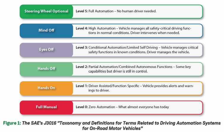
The SAE J3016 taxonomy describes five levels of vehicle automation. They range from level 0 with no automation, to level 5 which is fully autonomous and requires no driver at all. Moving up the chain to each higher level requires exponentially more processing power. The single biggest technology breakthrough that enabled the progress we are seeing today is AI in the form of machine learning (ML). However, within this field there are a large number of evolving technologies and architectures. Should processing be centralized or distributed? Should it use traditional CPUs or SOCs? In building autonomous vehicles major challenges have popped up concerning in-car networking bandwidth, memory bandwidth, ensuring reliability, and adaptability to evolving standards and required upgrades, among others.
Sensor data is exploding, expanding from pure optical sensors to proximity, LIDAR, radar, etc. Data needs to be combined using sensor fusion to create a real-time 3D model of the car’s environment that the vehicle can use to make navigation decisions. The natural outcome of this pressure is to place processing power closer to the sensors to speed up processing and reduce the amount of data that needs to be transferred to a central processing unit. This come with a side benefit of power reduction. Other data sources will include 5G V2V and V2X communication that will let cars exchange information and allow the road environment to communicate with the car as well. Examples of this might include information about traffic, road repairs, hazards or detours.
A new white paper by Achronix talks about meeting the power, performance and cost targets for autonomous vehicle systems. Often designers need to choose between CPU style processors or dedicated ASICs to process the information flowing through the system. However, there is an interesting third choice that can help build accelerators and offers adaptability in the face of changing requirements or updates. Achronix offers an embeddable FPGA (eFPGA) fabric that can be built into an SOC. Because it is on-chip, it can have direct high-speed access to memory and system caches. Their latest GEN4 architecture is targeted at machine learning applications, with special features for handing ML processing.
In addition to the obvious advantages that embeddable FPGA can offer, such as lower power, higher speed processing, ability to update algorithms in the field, or retargeting SOCs for multiple applications, it offers unique features for safety and reliability. As part of automotive safety standards, such as ISO26262, there is a need for frequent self-testing through BIST and other types of proactive test error insertion and monitoring. eFPGA can be reprogrammed during system bring up and even operation to create test features as needed. Another unique application for eFPGA will be in V2X communication implementation. When eFPGA is used in communication SOCs, it can be field updated to handle next generation communication protocols, like those in the upcoming 5G rollout.
The Achronix white paper outlines a number of other interesting ways that eFPGA can help enable the development of autonomous vehicle processing systems. It discusses how each instance can be specifically configured with the resources needed to perform the intended function. This eliminates some of the other problems with off-chip programmable logic – wasted real estate and mismatched resources. The white paper, which can be downloaded from their website, also offers interesting insight into how the market for autonomous vehicles is shaping up. I for one, look forward to the day that I can simply ask my car to take me home, instead of having to direct my full focus on the task of vehicle operation.