The Design IP market is doing well, growing at higher CAGR that the semiconductor market it is serving, in fact 10% higher for 2007-2017! You may wonder why this IP market is so business friendly? I will try to answer and propose the top 3 reasons explaining this behavior. To name it: IP business is recurrent, external IP sourcing is increasing penetration,and product ASP are constantly growing, for most of the IP. I will obviously develop and explain these statements (which are not necessarily obvious) and mention the mandatory conditions at which the vendors can benefit from these dynamics.
The Design IP, like the EDA business, is supposed to be recurrent. This means that you develop the product one time and sale it many times. This is completely true for the EDA business, but almost true for the IP business. Almost true because, when you consider the complexes IP generating high ASP (few $100K to several $ million), it’s very likely that the customer will request “some” level of customization. For a hard-wired IP (like a PHY), it may be a different lay-out option (North-South Poly orientation instead of East-West), or a modification allowing to fit with a different metal layers count.
When dealing with RTL IP, like a complex interface controller (USB, PCIe, Ethernet MAC or PCS,…) the possible modifications are multiple, usually to interface with a specific PHY, or with a different bus or application layer. Please note that this service is considered as IP customization, not design service. Why? Because the goal is eventually to sale your IP to this customer and not design service, and because you can re-sale it to a different customer.
By the way, design service business is by nature not recurrent, the reason why it’s by far less business friendly than IP business…
I should define that I mean by “business friendly”! If you want to rise funds for a start-up, you need to attract VC, and some businesses (or market) do it very well, and some don’t. This means that you must convince a VC that the investment will generate high return (x5 or even x10). If you look at the successful exit made by IP start-up during the last decade, you can name Virage Logic (sold to Synopsys in 2010), Denali (acquired by Cadence the same year) or Arteris sold to one of his largest customers, Qualcomm. In each case, the multiplication factor (acquisition price/last year revenue) was in the 6 to 10 range. Unfortunately, the data is not public, but I am very positive about these numbers.
If you don’t need VC, but want to create and develop a healthy business, we will see why the IP business is the type of business to target.
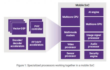
If you attend to a MBA, you will probably learn about ASP behavior: price premium at the product launch, then price stabilization for some time and price erosion. This model is true, especially for commodity products. But, if some IP products can be commodity (8051 for example), most of the IP generating high ASP are not commodity. We consider in this post the high-end, complexes, differentiatingIP addressing the modern SoC needs (CPU, DSP, GPU, memory controller, high-speed interfaces, Network-on-Chip and the like) which represent about 80% of the IP market value.
For these products, we clearly see an ASP increase over time, thanks to the continuous launch of new release (DDR3 then DDR4 and now DDR5 for example). This is surprising, and I was the first to be surprised when I built the first IP market surveys and realize that the ASP erosion model didn’t fit with the actual market behavior.
I can give you an excellent example with the PCI Express PHY. In 2005, PCIe 1.0 PHY (on 90 nm) was the state-of-the-art and selling for $150K. More than 10 years later, PCIe 5.0 PHY (on 10 or 7nm) is today selling for $1.5 million, or X10. But the PHY design is much more complex, deliver 32 Gbps instead of 2.5 and the technology has notably changed between 90 nm and 7 nm…
The controller (RTL IP) pricing is also increasing, at first due to the specification becoming much more complex at each new release and because the customers are usually asking for some customization. If we take the same PCIe example, but for the controller, the growth is more in the x3 to x5 range.
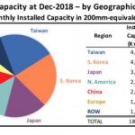
Another reason explaining the IP market growth is the externalization trend. In fact, the IP market mimic the behavior of the EDA market in the 1990’s. Every year, more chip makers are sourcing (more) IP externally. These two combined causes are explaining why the IP market has grown with 13.7% CAGR between 2007 and 2017 (see the first picture).
A good question is for how long this market will grow more than the market it serves, and how much will be the growth delta? It seems reasonable to forecast 2028 (+/- 1 year) as the year where the IP market will pass the TOTAL EDA market and probably reach asymptote. Nevertheless, this forecast is based on the IP market behavior during the last 15 years. IPnest think that this growth behavior should continue, at least up to the point of time where most chip makers will have decided to source IP externally, except for highly strategic IP, key to build differentiator. But these key IP only represent a very small portion of all IP integrated into a SoC. If we consider that the total number of IP can be one hundred (or even more), the key IP are limited to a very few % of the total.
The IP business is business friendly, and the future is bright, but there are some essential conditions to meet if you want to participate (there is no free lunch!). Ranking these conditions, one appears to be number one, and by far, it’s the high requested Quality level of the IP to launch on the market.
If you consider this IP from the user point of view, the quality means extended verification (running VIP for digital). If your IP is analog, like a SerDes for example, the customer will expect to see a test chip and a comprehensive characterization run on this test chip. Silicon proven is the magic word. Production proven is even better, but if the function is innovative, or just advanced, it’s likely to be too early to demonstrate it.
For certain IP, like PLL or DRAM memory controller, the function must be 100% error free: if it doesn’t work properly, the complete SoC development is wasted. The time to correct the bug, the customer will have missed the time-to-market, and most of his investment.
To propose the highest quality level, you need to build a strong engineering team, including at least an excellent architect, able to propose the best design solution. At the beginning of the 2000, we used to see IP start-up emerging and propose IP when they only had data sheet available. This time is over, and this is good news for professional IP provider and for customers!
Good product, strong engineering team are necessary but not enough. You also need to be able to propose good technical support. This means customer oriented and reacting fast support, based on FAE (who could also be part of the design team). Your customer will need these FAE to help him to integrate the IP into his design.
Now, when the technical offer is meeting the stringent quality requirements above describe, you could think that you’re done and neglect marketing… This is unfortunately a frequent mistake made by IP start-up who consider that building strong marketing and communication around their product is not necessary: they have the best IP! They just forget that the IP market is one of the fastest moving, if you leave this space uncovered, your competition will occupy it, even if your product is better.
If you don’t invest enough into market communication, nobody will do it for you. If you plan to use Rep to approach customers around the world, this sales force will need you to build the appropriate story and make noise about your product. If not, their task to convince customer will be just too difficult, and a Rep may give up and spend time selling other products… Building the right market communication campaign will be the next condition, right after technical quality, to turn your product sale into a business-friendly story or success story.
Last point, coming from 30 years experience in the semiconductor industry, equally split between chip makers (mostly ASIC) and IP. Both industries complement one another, but radically different, at least about the way to access the market. Chip makers are usually secretive and try to keep their development highly confidential, when an IP provider will try to maximize noise about their new product (sometimes before it can be available!). This has been one efficient strategy for companies like Denali, Virage Logic or Arteris, as they have been able to create very high market awareness (which has certainly helped to maximize revenues and exit).
IPnest is now 10 years old, and provide market surveys to many customers (more than 40, see the above picture), in Asia, America and Europe, from small to large IP vendors, chip makers, foundries or research center. These are demanding customers, expecting much more than simply vendor ranking or 10 years forecast, that we give. That they need is high quality data, accurate for actual data and realistic for forecast.
You can only provide these data if you understand the IP market dynamics, and to do so, you need to capitalize on long time experience about this market, knowing it from the customer view point (TI, Atmel) as well as from the provider (PLDA, Snowbush and my numerous customers). Excel is useful but not enough, the design, project manager and marketing experience are the only to give credibility, and that’s why IPnest is successful!
Eric Esteve from IPnest