webinar banner AI 2026 v2

Can I Trust my Hardware Root of Trust?

Can I Trust my Hardware Root of Trust?
by Bernard Murphy on 02-28-2019 at 7:00 am

Hardware Roots of Trust (HRoTs) have become a popular mechanism to provide a foundational level of security in a cell-phone or IoT device or indeed any device that might appear to a hacker to be a juicy target. The concept is simple. In order to offer credible levels of security, any level in the stack has to be able to trust that levels below it have not been compromised. The bottom of the stack becomes the root of trust. Given the sophistication of modern threats, most of us believe that has to be the hardware itself.

HRoTs aim to manage all security functions within a tightly-managed enclave. These would typically include functions such as secure key generation and storage, authentication, encryption and decryption and perhaps secure memory partitioning. The goal is to put all the security eggs in one basket and watch that basket very carefully rather than to scatter security features around a design and then not be sure what sneaky tricks an attacker might be able to use to get around those security measures.

So HRoTs are a good thing. And there are quite a few vendors who have excellent HRoT IP and will be happy to have you adopt their solution. Problem solved? Not exactly. You are going to integrate an HRoT into your larger design and, sadly, there are a number of ways this can go wrong. HRoTs are configurable because one fixed design can’t fit all possible needs, and when you can configure something you can configure it incorrectly. Second, you can make mistakes in hardware connections. Don’t laugh; some of these can be very subtle. Third, and most challenging, vulnerabilities at this level are not just in hardware or just in software; they can be in a combination of hardware and software. (For those familiar with the domain, think of timing-channel attacks on cache.)

Now you know that mistakes can happen, how are you going to find such mistakes? For the first two classes of problem, you might argue that a combination of hardware simulation and formal verification could do the trick. Maybe – problem is you first need to know what you’re looking for. But this debate is academic anyway because as soon as you need to cover hardware+software exploits, testing complexity explodes. Exploits can run over many instruction cycles and may use cache access times and other factors to accomplish their objectives. Mapping tests for any of this into standard hardware verification formats would be painful and is clearly impractical at a scale necessary to provide the comprehensive security coverage you need.

That said, you also clearly don’t want to have to setup a whole new verification infrastructure to solve these problems. What you’d like is a mechanism which can work with your existing verification platforms, particularly emulation since you’ll want to run software on your hardware platform. A good way to accomplish this would be through a class of assertions which can capture these security level checks but then be compiled in some manner into the existing verification infrastructure.

Tortuga Logic has created a nice approach to accomplish exactly this. I should say first that my explanation here approaches their technology bottom-up rather than a top-down presentation. But us hardware verification types may find it easier to understand. And this is just an example; talk to Tortuga for the full range of capabilities.

Any security check really comes down to proving there is no path though which something privileged (such as an encryption key) can flow to some unprivileged location (such as a USB interface). What is a little different from pure hardware approaches is that these “things” can be logical (data in memory locations) or physical (hardware). Tortuga has a format to describe and compile this kind of assertion into your standard verification environment.

A set of these assertions together represents a threat-model for the design; Tortuga Logic calls the language for these assertion “Sentinel”. This threat-model, together with the RTL, is compiled into a set of SVA assertions which you can run in any of your verification platforms, from formal to emulation (or even FPGA prototypes, I would guess, since they what they generate is an RTL model which runs together with your design).

So far, so good, but many users aren’t necessarily security experts; they invested in an HRoT because they wanted to avoid becoming experts. Doesn’t this verification requirement drag them back into needing to learn more about security? Tortuga just release a new update of their software, Radix-S, which aims to put more of this verification around HRoTs on auto-pilot. Jason Oberg (the CEO) told me they have helped draft guidelines and provide more features and guidance to setup the threat model and the flow for security novices. He tells me that even the experts like this flow because for them it adds automation; they know what they want but they don’t want to have to hand-craft it every time.

All of which is great, but for me the real deal-closer is the test-bench part of the story. Normally new simulation-based technologies can do great things only if you develop special-purpose test-benches to drive them. They sound good, but you have to do even more (and often rather specialized) test development work to tap the promise, greatly limiting their appeal. Not so with the Tortuga technology. The key differentiator in their approach is how they do the analysis – looking at information transfer through logic rather than logic states. They can do this based on your existing test suites. No need to develop new test-benches, just run what you already have together with their generated security-checking RTL. (Jason added, reasonably, that they do expect your test benches deliver reasonable coverage.)

So you can run advanced hardware/software checks on your existing verification infrastructure, using your existing test-suites. Difficult to imagine why you wouldn’t want to try that if you are even a little bit worried about security. Jason presented a workshop session on this topic Monday afternoon at DVCon. If you weren’t able to attend, you can learn more about Radix-S HERE.


How Well Did Methodics do in 2018?

How Well Did Methodics do in 2018?
by Daniel Payne on 02-27-2019 at 12:00 pm

In January I read from the ESDA Allianceabout EDA and Semiconductor IP revenues increasing 6.7% for Q3 2018, reaching $2,435.6 million, which is decent growth for our maturing industry. In stark contrast there’s a company called Methodicsthat specializes in Intellectual Property Lifecycle Management (IPLM) and traceability that has a much higher growth rate than the industry average. To get better informed I spent some time asking questions of two contacts at Methodics: Jerry Brocklehurst, VP of Marketing and Simon Butler, President and CEO.


Jerry Brocklehurst, Simon Butler

Q&A

Q: I know that you’re still a privately held company and don’t publish a detailed quarterly financial report, but what can you tell me about your growth rate?

Jerry: Well, we just reported 5 consecutive years of greater than 50% growth rate per year from 2014 through 2018.

Q: Wow, a 50% growth rate is way above the industry average. What trends are happening in the semiconductor industry that account for such rapid adoption of your IPLM tools?

Jerry: Over the past 5 years, semiconductor companies have found it mission-critical to implement design reuse strategies across their organizations in order to meet time-to-market, financial, and profitability goals while also facing tougher competition to design and produce ever more complex designs.

As design elements and IPs are being reused in different chips, a further challenge is the need to track all IP assets and to prove compliance with Functional Safety (FuSa) and security standards.

Q: OK, 2018 was another strong year, but what about 2019 for your business?

Simon: As we enter 2019, we see even more emphasis on the need for traceability as industry standards such as ISO26262, DO-254 and others are putting strict requirements for design traceability on suppliers. When customers create their designs within the Percipient platform, traceability can be easily achieved – it’s not an after-thought where assets must be tracked in spreadsheets or other manual ways. Traceability is a natural benefit of the Percipient methodology.

Q: Was there one particular geography that was adopting IPLM tools most?

Jerry: No, fortunately for us, we saw growth in revenue and in numbers of users in all regions, including the U.S., Asia/Pacific, and EMEA.

Q: Did you do anything different in 2018 at Methodics to help your customers?

Jerry: Yes, we had the first-ever Methodics User Groupmeeting with a keynote presentation by Intel and other presentations by Maxim Integrated, Silicon Labs, and Analog Devices.

Q: How about the way that your software integrates with other vendor tools in a design flow?

Jerry: Back in November 2018 we announced a software and technology partnership with Siemens, for a combined PLM/IPLM integration for our mutual customers. Late in 2018 we expanded our technology and reseller partnership with Perforce, providing a more tightly integrated solution for our semiconductor and embedded design customers.

Q: Can you give me a quick overview of your three tools?

Jerry: Sure, our Percipienttool is an IP Lifecycle Management (IPLM) platform that gives semiconductor design companies control over the design, integration, and traceability of internal IP, external IP, libraries for new analog and digital designs.

VersIC 2.0 Platform is a new approach to the management of IC design data. It provides a comprehensive, united and reliable design data management (DM) experience in the Cadence design environment.

WarpStoraddresses the issue in semiconductor design of data explosion by providing a Content Aware NAS optimizer and accelerator.

Q: Final question, why has Methodics been so successful in the IPLM arena?

Simon: From the beginning, our growth has been driven by our guiding principle to help our customers achieve success in their goals, and this past year was no exception. In addition to maintaining strong relationships with existing customers, we look forward to working with many new customers in 2019 and beyond.

Related Blogs


Safety: Big Opportunity, A Long and Hard Road

Safety: Big Opportunity, A Long and Hard Road
by Bernard Murphy on 02-27-2019 at 7:00 am

Safety, especially in road vehicles (cars, trucks, motorcycles, etc.), gets a lot of press these days. From the point of view of vendors near the bottom of the value chain it can seem that this just adds another item to the list of product requirements; as long as you have that covered, everything else remains pretty much the same in your business cycle. That would be nice but it’s quite inaccurate at least for those selling components, such as IP, which wind up in the final product.

Back in the mists of time (5 years or so ago), vehicle electronics were pretty simple: a number of small control units, simple 16-bit or maybe 32-bit MCUs, spread around the car to handle braking, engine control chassis control and so on. Then we all got excited about putting more intelligence into our ride. Automakers started with automated driving assistance – lane keeping, intelligent cruise control and the like. This takes real compute horsepower, far beyond the capabilities of an MCU. And decisions you want these engines to make, such as, “should I brake because I see a pedestrian crossing the road”, can’t be distributed around the car. So the next logical step was to architect for a central brain, digesting sensor input from around the car in support of its decisions.

Which in part drove the need for Automotive Ethernet, because that’s a lot of data you have to send – just think of a video stream from a camera. And we realized we needed a lot of these sensors, partly to cover different directions but also for different capabilities – more cameras, radar and lidar for ranging and speed information for objects around the car and ultrasonic sensors for parking control. Each pumping masses of data to that central brain to drive time-critical decisions.

Hmm – maybe need to rethink the architecture a bit. So we are now adding more intelligence to the sensors, increasingly in ASICs for performance, so they can just send back object lists rather than raw images to reduce the load on the Ethernet. But that’s not quite right either because sometimes we want both objects and images – detect a pedestrian but also show the image on the cabin monitor so the driver can decide if she thinks there’s really a problem or not. Then there’s sensor fusion; maybe recognition needs to look at both the camera and radar images, not just objects, to draw a conclusion. Bottom-line, there is no “right” architecture – central or distributed or a mix – at least today, so OEMs pick candidates which best serve their competitive and safety needs. Here, Safety of the Intended Function (SOTIF, beyond 26262) is also becoming more prominent although it’s unclear yet how this will affect hardware developers; it would be surprising to hear it will have no impact.

Then you get down to building these chips for which you have to ensure functional safety. Systematic errors are dealt with through the process side of ISO 26262 on which I and others have already written plenty. Random errors triggered by cosmic ray-induced ionization are also a concern. Back in those same mists of time, processes use for automotive electronics were, per Kurt Shuler (VP marketing at Arteris IP) “Cro-Magnon”; 50nm or thereabouts, less susceptible to this kind of problem. But you can’t build these big ML-centric chips in 50nm; ADAS devices are now going into 7nm where ionization is much more of a problem. In your phone or TV, this is not a big deal, but in a safety-critical system random errors have to be weeded out, at minimum by detection, better still by correction. In ISO 26262 Part 2, you and the integrator need to deliver credible evidence that the safety mechanisms provided are sufficient.

Since I’m talking about Arteris IP, the interconnect between CPUs and ML accelerators and all the other goodies in these big devices, this runs to tens of millions of gates itself, a major candidate for random error detection/correction. This can be through parity checks, ECC or even logic duplication with units running in lockstep. Though of course where to insert such mechanisms rests on decisions the integrator will make based on failure mode effects and diagnostic analysis (FMEDA) with planned detection/mitigation fixes. A network-on-chip (NoC) interconnect is built bottom-up so the safety mechanisms can be programmed in, as needed, bottom-up. Other IPs will often have to work harder to provide similar levels of protection (and confidence); retro-fitting safety is a lot harder than designing it in from the outset.

So far, so complicated, though maybe no big surprises above what you already knew. But now look at the support and business cycle from an IP vendor point of view. During design, the vendor supports the integrator in joint discussions on how to meet functional safety goals with respect to that IP and helping the architect and integrator as needed. The integrator tapes out, when everything goes relatively quiet for maybe a year or more as the integrator works with their customer, maybe a tier 1. Then requests start rolling back to you; the integrator wants to know more about how something was designed, for verification reports and confirmation measures and you have to support them in their responses. Point being that “signoff”, measured by when you get paid, moves higher in the chain and later. Kurt said they have seen 5-6 years in one case, although competitive pressures are driving that down somewhat. Royalties as always come later still. Another twist; IP vendors now have to keep everything that was built in a lock box for 10 years.

Still think you want to sell IP into the automotive chain? There’s certainly a lot of promise. More big chips in the central brain and in intelligent sensors together offer a lot of opportunity. The US, Europe and Israel markets are all very aggressive in developing ADAS and ML. China has been a laggard but is coming on strong and is not held back by legacy so much. They also see a big tie-in with AI where they are very strong. Kurt tells me there are over a couple of hundred funded startups in automotive and AI in China.

That said, this is not an easy way to get rich. You’ll have to put a lot of investment into supporting your customers, supporting their customers and so on up to the top. The market is very dynamic, so what “done” means may not always be clear. You may not be paid for quite a long time. But if you have the grit to hang on and keep your customer happy the whole way through, you might just be successful!


eSilicon Expands Expertise in 7nm

eSilicon Expands Expertise in 7nm
by Tom Simon on 02-26-2019 at 12:00 pm

At SemiWiki we usually don’t write about the press releases we are sent. However, a recent press release by eSilicon caught my eye and prompted me to call Mike Gianfagna, eSilicon Vice President of Marketing. The press release is not just about one thing, rather it focuses on a number of interesting things that together show their momentum, especially in the 7nm space. So, in my conversation with Mike I dug a bit deeper to better understand their progress. 7nm is a topic that gets a lot of talk, but eSilicon can point to some pretty significant and very real milestones at 7nm.

Not that long ago eSilicon announced their NeuASIC IP platform that targets AI designs at 7nm. It offers specialized AI blocks that perform convolution operations and acceleration of AI tasks. Also included in this are HBM2 PHY IP. Similarly, they recently announced their 56G long reach 7nm SerDes. In talking to Mike, he was quick to point out that If you look at AI designs, they have moved memory from large instances to localized memory associated with each processing element. This helps eliminate memory access bottlenecks that these designs are prone to.

In many cases 50% of the area on AI chips is dedicated to memory. Interestingly, about 250 of eSilicon’s 500 person design team is focused on memory design. In short, they have significant resources to apply to these leading-edge memories. This is big leverage point for reducing power and area.

Another focus of Mike’s comments had to do with what it takes to deliver silicon for today’s systems. He pointed out that Apple early on figured out that the processor chip was a big differentiator for their products. We now live in an age where most of the big systems companies are well aware that the SOCs that go into their designs are critical to product success and differentiation. This is why we see many very large systems companies driving SOC development. So, it goes without saying that these are type of companies that would look to eSilicon for ASICs to incorporate into their products.

However, delivering silicon to systems companies results in a totally different kind of engagement than there used to be for earlier ASICs. At 65nm each team could engage sequentially. You had the front-end guys in at the kick off and brought test in later closer to the end of the cycle. No longer. The criteria for success now is having the chip working in the targeted system, not just delivery “to spec”.

Mike said that the project kick-off teams now have “all hands” to ensure that each phase of the project will run smoothly. Another example of this phenomenon is that the bring up team from eSilicon is at the customer several months ahead of silicon delivery to look at firmware, test methodology, etc.

Mike and I also spoke about SerDes design and how it has changed over the years. Mike says their customers need to measure the SerDes performance completely isolated from all the test fixtures and equipment. This is a big task given the high frequencies and tight tolerances. This is why they partnered with Wild River to develop a test board to allow de-embedding. A 56G SerDes still is very much dependent on the package, board, connectors and cable for its performance. So, in a way the test board best practices can serve as a reference design to help guide system integration.

The current generation of SerDes will actually monitor its own performance and adapt to the operating environment. eSilicon uses a RISC-V processor core inside the digital section of their SerDes to control its operation. It’s even possible to open up a graphical interface to the internals of the SerDes to view its functioning.

eSilicon now has silicon back for two different advanced FinFET designs and is going through bring up. These chips incorporate advanced IP – high speed SerDes, specialized IP, advanced memories, 2.5D HBM, advanced packaging, etc.The effort required to build an effective platform for SOC design at 7nm is immense.eSiliconhas worked hard to achieve success at previous nodes such as 28nm, 16/14nm and now on 7nm.This is the kind of silicon that will be used in data centers, automotive intelligence and other demanding applications. For more background on their progress take a look at the press release on their website.


Interview with Bob Smith, Executive Director of the ESD Alliance

Interview with Bob Smith, Executive Director of the ESD Alliance
by Daniel Nenni on 02-26-2019 at 7:00 am

Bob Smith is executive director of the ESD (for electronic system design) Alliance that many Semiwiki readers will remember as the EDA Consortium. As Bob explains, the semiconductor industry is changing and evolving, and the electronic system design ecosystem with it. I encourage you to take a break from what you’re doing and read about the ESD Alliance and the new event, ES Design West.
Continue reading “Interview with Bob Smith, Executive Director of the ESD Alliance”


Mentor Automating Design Compliance with Power-Aware Simulation HyperLynx and Xpedition Flow

Mentor Automating Design Compliance with Power-Aware Simulation HyperLynx and Xpedition Flow
by Camille Kokozaki on 02-25-2019 at 12:00 pm

High-speed design requires addressing signal integrity (SI) and power integrity (PI) challenges. Power integrity has a frequency component. The Power Distribution Network (PDN) in designs has 2 different purposes: providing power to the chip, and acting as a power plane reference for transmission-line like propagating signals. One must pay attention to traces going from one layer to the next and to return current flowing on one power plane, when return current has to jump to another plane somehow. The challenges include PI, SI, return path analysis, EM modeling and an understanding of metal and dielectric structure. HyperLynx solves those challenges.

A vast bulk of designers do not know how to do this high-speed analysis, getting to a point where experts are needed. Todd Westerhoff, HyperLynx product manager, calls it the ‘expert bottleneck’ during a chat at DesignCon 2019. He states “With signal integrity design challenges, it is harder to find the expert and the time. HyperLynx relieves the need to have a dedicated SI person. Point tools offer the best in this and that. HyperLynx brings all this together. If you are designing a 112G device and wondering how to perform the complex analysis, with a signal out of one device on board, through a via and off, you will look at each part of the signal hierarchy. How does the field behave? You do not decompose at all and put into an electromagnetic solver, as this is too big of a problem. You can section it, and bring it back together. Can you do a distributed analysis? You can look at a whole path and break the trace into different segments and make it a 2D problem, but when you go through a via and board coupling, it becomes a 3D problem. The current next to a via becomes irregular. Far enough from a via, you get a constant cross-section and solve through the disruption. This is not complicated, it is standard housekeeping, but it becomes difficult not to make mistakes. HyperLynx takes care of that.”

When modeling interconnect, you bring the board database from the CAD system, the tool looks at the layout, and finds where the nets are. EM analysis produces S-parameters. Once the channel is modeled, the simulators become simulator specific but are still agnostic on the data format.

HyperLynx is a suite of tools which include signal integrity (SI), power integrity (PI), an electromagnetic (EM) solver, a DRC expert rule-based checker for problems like thermal issues. In rules-based geometry checking (DRC), the checks return currents in terms of signal propagation. Usually, PCB designers manually review the database and sometimes they eyeball the layout and turn on traces. The problem is that it is easy to miss something. Pattern-based, DRC geometry checking extended to many levels, EM modeling, simulation, and modeling technology are needed. The goal is reading the layout and checking for common problems without modeling all the IO. There are limited ways to do what-ifs and doing an incremental analysis. Some items to note:

● There is a pre and a post route signal integrity analysis distinction: Pre-route is what-if, post-route is verification and validation.
● All tool modules are integrated so patch releases are in one release.
● HyperLynx is leading in making simulation easy to use while preventing costly repairs.
● One can open HyperLynx from within Xpedition. HyperLynx has the ability to create reports for certification including electrical safety compliance.
● There is a big gap between how many SI and PI experts are needed and how many are available. With the pervasive expert bottleneck, the problem is getting worse, thus the need to take sophisticated analysis to a broader audience. Managing expert availability is always a challenge. Using the analogy of vinyl records, Westerhoff quips ‘you want the needle to stay on the record, but it keeps skipping’.

Reducing Certification Risks

One of the increasing challenges for system, board and chip designs is comprehensive automated design checking and verification while meeting the increasingly demanding certification requirements. Manually verifying a schematic, layout and prepping for manufacturing is time-consuming. IEC safety standards need to be met and power and signal integrity issues need to be addressed in a timely fashion.
These verification tools work in any flow and can be sold standalone. However, their integration with Mentor’s Xpedition flow has an advantage. This allows the person performing the schematic capture or layout design the ability to fix the errors without the usual back and forth of simulation and without adopting a new tool.

Automated Design Compliance Testing with Xpedition Validate features include:

● Fully automated proven schematic integrity tool designed to replace visual inspection
● Exhaustive power and technology aware test of all schematic nets
● Parametric error detection
● Warnings highlighting poor design
● Major EDA tools agnostic
● No additional infrastructure required
● 150+ automated checks
● 6+ million library parts

Examples of checks performed include:

● Open collector/drain
● Poor practices (lack of needed pull-ups/pulldowns)
● Power/ground connectivity
● Component power checks
● Multiple or missing power supplies
● Differential pin checks
● Unconnected nets or buses
● Off-board net collection
● Overloaded pins
● Unconnected mandatory pins
● Nets missing driver
● Diode orientation

HyperLynx Scalable High-Speed System Design

A study of 100 customer designs showed that direct savings exceeded $51K per project and of those 100 designs, 69 were spared a re-spin with 18 time-to-market days reduction.

● After models are assigned, the designer can scan for voltages on the nets or export from CSV format.
● The IEC standards are embedded in the rules.
● Automatic checks such as output threshold can be run.
● Power net checks decoupling caps detection, return path reference point changes.
● HyperLynx DRC can be run inside layout, can check 3D, multilayer creepage, a big safety issue.
● Automating manufacturing Valor does those checks, allowing a move from proto to production.
● Will check weak solder joints, flex conductive materials, manufacturing issues.
● Valor includes 35 million industry standard manufacturing part numbers and will do a virtual prototype of the build. Valor can also be run inside the layout tool. If constraints are changed, Valor will read these changes dynamically and update.
● Automated compliance checking for schematic, layout and manufacturing.

Physical Design Checks Certification Risk Reduction with Valor NPI

HyperLynx Model-Free Analysis Flow

An automated Design Rule Check finds and fixes marginal and questionable practices and identifies simulation issues before embarking on a detailed analysis which checks common design decisions and applies standards-based verification followed by silicon-accurate verification that would allow signoff. This simple screening for errors and the use of protocol models minimizes expensive vendor-specific simulation and lengthy runs.

The power-aware simulation includes 3 separate types of Signal Power Distribution network (PDN) interactions:

● Multiple driver switching and power supply effects
● Via-to-via coupling through PDN cavity
● Non-ideal trace return path effects.

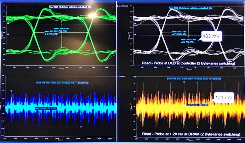
This power-aware simulation reduces overdesign and reliance on guidelines that may add design cost and complexity. Another benefit of power-aware simulation is the ability to make design tradeoffs for high-volume, low-cost, layer and space constrained designs.

Power-Aware: HyperLynx DDRx Design Flow

With the ability for the designers to do their own validation, the experts are freed up to focus on more complex multi-physics analysis for specific tough problems. This best practice allows shortened design cycles, reduced re-spins and higher product quality with errors caught early in the design cycle.
Mentor automated design compliance testing tools reduce certification risk with shorter turnaround time due to the following:

● Automated tools from Mentor allow every net, component, or scenario in a design to be checked, and are not just limited to critical areas the designer has time to check
● These tools work in any flow and can be sold standalone. However, their integration with Mentor’s Xpedition flow provides an advantage. This allows the person performing the schematic capture or layout design the ability to fix the errors without the usual back and forth of simulation and without adopting a new tool since the compliance testing works with current Xpedition GUIs and Xpedition format
● Certifications issues are identified in real-time, not at the end of the design cycle.
HyperLynx and Xpedition flow allow model-free analysis, power-aware simulation well suited for high-speed design, ensuring reliability, safety compliance with reduced cycle-times and certification risk in a cost-effective way.

[More information on HyperLynx]


Delivering Innovation for Regulated Markets

Delivering Innovation for Regulated Markets
by Daniel Nenni on 02-25-2019 at 7:00 am

When delivering devices to markets that require heavily audited compliance it is necessary to document and demonstrate development processes that follow the various standard(s) such as IEC65108, IATF16949, ISO26262.

For complex multi-disciplinary designs this can be difficult as they are often developed by multiple teams in different locations. Additionally, hardware and software IP is frequently supplied by other groups or 3[SUP]rd[/SUP] party organisations. To further complicate matters, disparate sets of tools often are used to develop the devices and included IP. Nevertheless, at the system integration level there is a need to manage functional and technical requirements, and to trace the safety and compliance goals or requirements throughout the design, verification and validation steps.

‘Requirements driven verification’ is a methodology which is baked into these standards, ensuring that requirements are adequately verified by connecting them to verification tasks.

As an example, the ISO 26262 standard for automotive electronics systems requires that a dedicated qualification report needs to be provided along the hardware component or part that documents the appropriate safety requirements. The qualification report demonstrates that the applied analyses and tests provide sufficient evidence of compliance with the specified safety requirement(s). The relevant failure modes and distributions also need to be included to support the validity of the report.

The safety requirements can be authored in any number of systems such as Doors, 3DEXPERIENCE, excel, word, pdf, etc. Furthermore, technical requirements for the design may exist in many other information systems. For instance software, digital and analogue teams use different IDEs and tools like JIRA to manage their development process. The ability to trace and follow of all these requirements from disparate heterogeneous information systems is needed to efficiently synchronize the validation.

Figure 1 shows an example of this type of traceability using the 3DEXPERIENCE platform. It provides a birds-eye view in which high level information is displayed, giving users a view of the instantaneous status on the coverage for their project, and the ability to quickly navigate to the source System of Record for the information.

Figure 1

The view in figure 2 drills down to a more detailed representation, giving engineers information on what is already covered, what is still uncovered and their status at each level of the project. It provides flexible navigation from one project artifact to another.

Figure 2

In addition it is important to be able to maintain a history of the different project stages. These are called snapshots in the system traceability tool, which are read-only versions of the project stages. They are mandatory to monitor project progress and to answer questions like: What requirements have changed? What are the impacts on my development and testing? How is the coverage of my requirements progressing? These snapshots could be linked to project milestones and can generate the traceability matrix for each milestone or product delivery.

3DEXPERIENCE offers essential features necessary for complying with safety and reliability standards, such as those found in the automotive industry. For devices developed for these markets, there are a number of deliverables that are essential. Primarily they relate to documentation that ties specific features back to initial safety requirements. With large dispersed development teams, it is necessary to have a unified system to provide traceability and help generate documentation that supports final system qualification. More information about how to help meet compliance requirements for semiconductors is available on the Dassault Systèmes website.

Also Read

Webinar: Next Generation Design Data & Release Management

IP Traffic Control

Synchronizing Collaboration


Verifying Software Defined Networking

Verifying Software Defined Networking
by Daniel Payne on 02-22-2019 at 12:00 pm

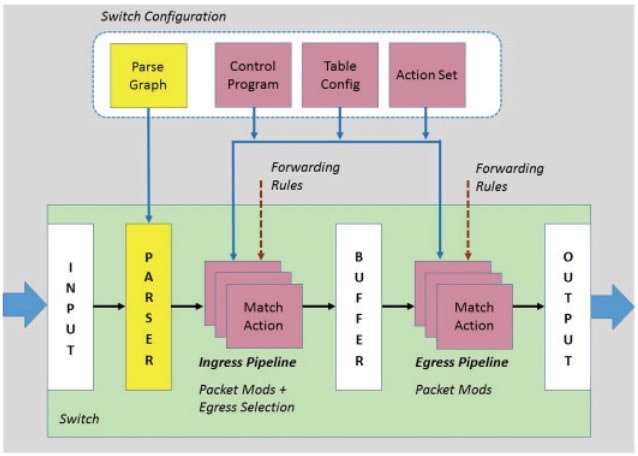
I’ve designed hardware and written software for decades now, so it comes as no surprise to see industry trends like Software Defined Radio (SDR) and Software Defined Networking (SDN) growing in importance. Instead of designing a switch with fixed logic you can use an SDN approach to allow for greatest flexibility, even after shipping product. For SDN the key feature is the configurable match action devices as shown below in the plum color:


SDN abstract forwarding model

Downloading a new configuration into a SDN device is typically through a Peripheral Component Interconnect Express (PCIe) interface, and can involve using a Virtual Machine (VM) over PCIe. There are many unique challenges in verifying the HW and SW for a SDN system:

  • Forwarding elements changing based on traffic type and service class
  • Load balancing
  • Performance monitoring
  • Operator control
  • Validating drivers and applications
  • Compliance of SW drivers with orchestrators
  • Handling data plane exceptions

Let’s look at some different approaches of using PCIe as the management port for verifying a modern SoC device like an SDN. The control and forwarding tasks are separated in SDN devices as shown below:


Example SDN HW Block Diagram

Everything shown above in blue can be configured, even on the fly. The Orchestrator configures the networking data plane and manages a single chip or multiple chips using a processor. SDN devices have a wide range of tasks:

  • Service routing
  • Bridging
  • Forwarding
  • Replication
  • Network Address Translation (NAT)
  • Multi-protocol Label Switching (MPLS)
  • Data Center Bridging (DCB)
  • Virtual extensible Local Area Networks (VXLAN)
  • Network Virtual General Record Encapsulation (NVGRE)
  • Generic Network Virtualization Encapsulation (GENEVE)
  • Spanning tree protocols

A vector-based verification (VBV) methodology could be used in different ways:

[LIST=1]

  • Software VBV
  • UVM
  • Advanced VBV

    With Software VBV the SDN SW creates a configuration and that gets played in your simulator/emulator tools using a PCIe transactor as shown below. The Mentor PCIe Transactor has a Direct Programming Interface (DPI) and Veloce Transaction Library (VTL) API:

    On the left-hand side are High-Level Verification Language (HVL) components that talk through the C Proxy layer and Extended RTL (XRTL) FSM.

    A second approach using UVM has data streaming to PCIe transactors or Bus Functional Models (BFM) from directed tests.


    UVM Topology in support of Emulation

    The downside of UVM VBV is that UVM is the test executor with SystemVerilog, and there isn’t a direct connection to SDN management SW. UVM VBV with an emulator is called testbench acceleration.

    Verification with Advanced VBV (AVBV) has the SDN DUT connected to the Software Development Kit (SDK) HW. The limitation here is that co-verification between product SW and HW is not provisioned. This methodology used with an emulator over IO is called In-Circuit Emulation (ICE).

    VBV issues from these three methodologies include:

    • Large Memory Mapped IO (MMIO) spaces create overhead
    • Slow simulation speeds

    To overcome the limitations there is a better way, and that’s with an approach using Virtual PCIe because applications can interact with the emulation DUT as if it was the actual silicon, enabling HW/SW co-verification. The SDN device will be operating slower in the emulator versus final silicon, but orders of magnitude faster than simulation, yet sufficiently fast for co-verification and debugging.

    Here’s an example showing a Virtual Machine (QEMU) running Linux, Red Hat or SuSE OS:


    VirtuaLAB PCIe3 Control and Data Path Overview

    VirtuaLAB is a virtual PCIe RC from Mentor, and the library already supports:

    • Networking
    • Multimedia
    • Storage
    • Automotive
    • CPU

    The PCIe Software Under Test (SUT) driver in this approach is identical to what a customer receives, so no more surprises between pre and post silicon.

    Now your engineering team with VirtuaLAB PCIe can take a parallel development path with product SW/drivers and HW, instead of a much-longer serial process waiting for silicon. Remember, with the AVBV approach you couldn’t test functional SW APIs, but they can be tested with VirtuaLAB PCIe. Some key features to know about with VirtuaLAB PCIe are:

    • Checkpoint save/restore
    • Protocol analyzer
    • Modeling flexibility
    • Advanced debugging

    One user compared this emulation approach versus a device on the bench, reporting that 15 seconds of SDK in real time took about 30 minutes in the emulator.

    All transactions between host and emulator are visible, making for quicker debug. There’s even a protocol analyzer that is similar in appearance to a LeCroy PCIe analyzer, providing statistics and tracing features:


    VirtuaLAB PCIe Protocol Analyzer

    Conclusions
    Modern SoCs like SDN devices are incredibly complex in terms of verifying both HW and SW, and the traditional Vector Based Verification (VBV) methodologies can fall short. Using the newer, virtual methodology with tools like VirtuaLAB PCIe from Mentor are more productive. Read the complete 10 page White Paper here.

    Related Blogs


  • Low Power SRAM Complier and Characterization Enable IoT Applications

    Low Power SRAM Complier and Characterization Enable IoT Applications
    by Tom Simon on 02-22-2019 at 7:00 am

    If you are designing an SOC for an IoT application and looking to minimize power consumption, there are a lot of choices. However, more often than not, looking at reducing SRAM power is a good place to start. SRAMs can consume up to 70% of an IC’s power. SureCore, a leading memory IP supplier, offers highly optimized SRAM instances for such applications. They took the approach of looking at first principles to effectively rethink how to reduce SRAM power. Making good use of their approach, they have developed memory compilers that deliver front and back end views of the memory instances required by their users. As part of this, accurate timing and power views are needed to complete designs incorporating these instances.

    Designers utilizing SRAM instances look to Liberty model files to provide characterized timing and power information so that system level simulations are fully accurate. Generating this characterization data is computationally intensive according to sureCore. However, they make use of advanced tools and techniques to make the task manageable. In my conversations with them they discussed how they manage the characterization process for their EverOn 40ULP family of SRAM instances.
    For each synchronous input, for a range of clock and data edge speeds (typically around 7 of each) they needed to examine 49 (7×7) setup and hold values. On the power side, they needed to look at static and dynamic power for operation modes such as read and write, as well as the full range of available power down and sleep modes. As you can see, this becomes an exponentially growing problem since different PVTs are added and consideration is given for each of the different configurations.

    The EverOn[SUP]TM[/SUP] family consists of 276 different SRAM instances that vary in aspect ratio, word count and word length. The family’s operating range is between 0.6V and 1.21V, creating a large PVT space for full characterization. A brute force approach to simulation could easily require an unworkable 24 hours per instance. One aspect of their characterization solution is to take advantage of the most recent and advanced features of Liberate-MX provided by Cadence.
    (Note: Is this too much of an ad for Cadence?)

    They explain how several features in Liberate-MX accelerate the process. First Liberate-MX can carefully prune the netlist during timing estimation to include only the circuit elements necessary to provide an accurate value of the timing parameter being characterized. The other technique they employ is using interpolation to provide power numbers over a wide range of memory configurations. SureCore has used full characterization runs on sample memory sizes to validate the interpolation results and has seen excellent correlation.
    The Cadence tool suite is used to optimize runtime while maintaining accuracy. Liberate-MX cleverly dispatches leaf level pieces of the memory instance to Spectre XPS for detailed SPICE simulation results. With smaller process nodes there has been an increase in PVT corners, and Monte Carlo analysis is becoming necessary. The number of simulation runs needed has exploded. They use the new Cadence Super Sweep technology, leveraging simulation steps that can be shared between different corners that accelerates simulation. SureCore has seen a 2x speed up in runtime and an improvement in accuracy using these techniques.

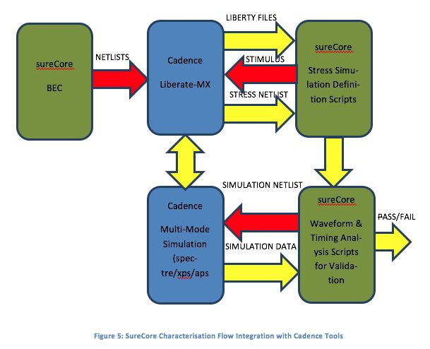
    However, a substantial part of reducing their computational requirements for memory characterization come from the flow that sureCore has developed, including specific parasitic reduction techniques to deliver optimized netlists that provide optimal inputs to each step in the flow. They report dramatic reductions in netlist sizes for timing, static and dynamic power.

    SureCore also focuses on validation to ensure the characterization flow is producing safe and accurate results. They have a scripted environment to check simulation results to ensure that the models perform properly. They even run checks that validate that the correct internal structures were included in the characterization runs. On top of this they run stressed simulations with Monte Carlo variation.

    SureCore is filling a need for low power SRAM IP, which is critical for a variety of edge devices in a plethora of applications. I found it fascinating to learn about their comprehensive process dedicated to characterization. They have white papers on their website that offer interesting information on their technology. Without a flow like this, it would be a computational challenge to deliver high quality and consistent IP deliverables in a reasonable timeframe.

    You may want to check-out more about this unique characterization methodology by clicking here or going to www.sure-core.com.


    Accelerating Post-Silicon Debug and Test

    Accelerating Post-Silicon Debug and Test
    by Alex Tan on 02-22-2019 at 7:00 am

    The recent growing complexity in SoC designs attributed to the increased use of embedded IP’s for more design functionalities, has imposed a pressing challenge to the post-silicon bring-up process and impacting the overall product time-to-market.

    According to data from Semico Research, more than 60% of design starts contain IP reuse and the number is expected to increase due to the high silicon demand related to today emerging applications such as 5G wireless communication, autonomous driving and AI.

    Based on data from Gartner, the staff-years equivalent effort for designing a 7nm SoC is more than 5 times than those of 28nm. The cost to testing the associated IPs is also on the rise. To mitigate this post silicon validation and debug challenge, design teams have resorted in applying on-chip debug strategy, more automated techniques for post-silicon test generation and pre-tapeout assertions for effective coverage/analysis. For example, on-chip buffers is deployed to improve observability and controllability of the internal signals during trace-based debugging.

    The traditional silicon bring-up and debug flow has been inherently inefficient as it involves multiple translations of test related collaterals. In this scenario, a DFT engineer or designer initially uses a mix of document based test descriptions and simulation generated tests to handoff the testing directives to the test engineer, who will then reformat them to the ATE of choice for silicon validation. The subsequent test generated results is then re-translated back into tool format used by the DFT engineer for review. Such iterative process is prone to delays as access to testers may be interrupted while run data being process for assessment.

    IJTAG (Internal Joint Test Action Group) or IEEE 1687 provides an access standard to the embedded instruments and allows vector and procedural retargeting. It incorporates the mainstream IEEE 1149.1-x and the design-for-test standard IEEE 1500. Since its introduction in 2013, the IJTAG based adoption has been on the increase. The JTAG TAP (Test Access Port), a five-pin, state-machine based interface, not only controls the boundary-scan logic and tests, but it has been used to access more embedded instruments and IPs.

    IJTAG creates a plug-and-play integrated environment and use of the instrumentation portions of IP blocks which includes test, debug, and monitoring functions. Part of the standard includes two languages: first, ICL (Instrument Connectivity Language) hardware rules related to the instrumentation interfaces and connectivity between these interfaces; and second, a Tcl-based PDL (Procedural Description Language) that defines operations to be applied to the individual IP blocks. While ICL is an abstraction of the design description needed to scan read/write from/to the instrument, PDL defines the syntax and semantics of these operations. The PDL may be written with respect to the instrument’s I/Os and is also retargetable. Retargeting translates the operations from the instrument through hierarchical logic described in ICL up to the top level of the design.

    Even though IJTAG streamlines IP integration during the design phase, frequent third party related IP evaluation and debug issues still persisted during silicon bring-up –thus affecting the production yield ramp-up. To address this issue, Mentor’s Tessent SiliconInsight with ATE-Connect™ technology paired with Teradyne’s PortBridge for UltraFLEX, to enable DFT engineers to directly control and observe IPs in the SoC-under-test on the ATE. This solution resolves a number of key problems of an IJTAG-based IP evaluation and debug. It delivers a protocol-based flow instead of a pattern-based flow using IJTAG commands, and utilize Tcl-based Tessent shell interface to access ATE unit remotely through TCP connection. Another Tessent’s tool SimDUT to allow users to debug and validate the PDL procedures and related Tcl procedures

    Figure 4 shows an example on how the environment is being utilized. The MBIST engines at the upper right are being accessed and controlled through the IJTAG. Similarly, the debug of two mixed signals IP blocks, DAC and ADC can also be achieved through the same approach. Tessent SiliconInsight tools could address both the test engineer need of having a fast and reliable test to optimize yield and minimize test cost, and the DFT engineer interest in confirming the functionality and critical metric extraction.
    Initially, the test engineer can configure the ATE and perform proper setup/biasing of the DAC/ADC blocks. Once setup is completed, the test engineer passes control to the DFT engineer to run the previously designed tests or to do any needed interactive debug. Upon verifying both IP blocks, the external ATE resources can be optionally replaced with a less costly loopback connection mode. Running subsequent what-if testing, applying different adjustment on the adjoining block such as PLL and reassess system level functionalities can be done. Both the DFT and test engineers viewpoints are aligned (while they might not in the same geographical locations), enabling also pattern generation need or using ATE-Connect to target a bench setup with the debugged tests –streamlining further the three environments (design, test, bench) to accelerate time-to-market.

    The takeaway from having Tessent SiliconInsight with ATE-Connect technology is that it delivers efficiencies in silicon bring-up, post-silicon and IP debug or evaluation. The simplified IJTAG based standard also provides DFT and test engineers with option to scale their IP testings.

    For more info on Tessent based test flow, check HERE.