Mentor put on a very interesting tutorial at DVCon this year. Commonly DVCon tutorials center around a single tool; less commonly (in my recent experience) they will detail a solution flow but still within the confines of chip or chip + software design. It is rare indeed to see presentations on a full system design including realistic use-case development, system design and end-application validation together with an electro-mechanical model. That’s what Mentor presented in this tutorial and my hat is off to them. Obviously synergy with Siemens is starting to have an impact.
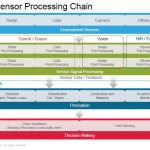
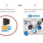
Jacob Wiltgen (Mentor, all the speakers were from Mentor) kicked off by outlining their goal for a level 4/5 autonomous car: to develop a computer vision system from scratch, to functionally verify that systems and optimize for PPA, to plan, measure and integrate safety into the system to meet an ASIL-B safety goal and then to validate the operation of that system in a digital twin all the way from sensing in simulated but realistic driving scenarios, through compute (recognition) to actuation, electro-mechanically simulating braking. In this case the goal was to detect a pedestrian in the highway and apply the brakes autonomously.
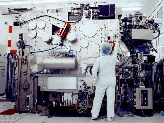
David Aerne started this flow with a presentation on using high-level (C++) synthesis to build a CNN recognition engine. It’s pretty clear that architectures in this space are very dynamic; in automotive applications where response time and accuracy are paramount, it would not be surprising to see a lot of custom implementations. HLS, often associated with image and similar processing functions, is a natural fit for CNNs. Optimizing the CNN to an application involves many architectural tradeoffs – number of layers, pooling choices, sliding window architecture, memory architecture, fixed point word-sizes at each layer, … Trying to manage this at RTL would be impossible, but is a natural process in C++ using abstraction/complexity-hiding to be able to easily compare alternative implementations. Another very important advantage that comes with design at this level is that you can also verify at the same level. Which means you can verify against very large image databases, orders of magnitude faster than would be possible in RTL.
Jacob followed to talk about the functional safety part of this flow. This is a topic that gets a lot of coverage, so I’ll just pick out a few points that struck me. First this is clearly an area of strength for Mentor. They have the broadest range of tools in this space that I have seen:
- Safety analysis through SafetyScope (through acquisition of Austemper) – still relatively unchallenged in EDA as far as I know
- Design for safety through Annealer and Radioscope (also from Austemper) and Tessent BIST
- Safety verification through Kaleidoscope (again Austemper), Questa Formal, Veloce FaultApp and Tessent DefectSim
- Lifecycle management through Siemens Polarion and Questa verification management
Through this suite of tools, they are able to do early safety exploration, estimating what level of diagnostic coverage may be realistically achievable. Then they can automate insertion of planned safety mechanisms and assess their PPA impact. Finally they can plan a fault campaign for FMEDA analysis, classifying faults and grading and filtering tests to optimize fault simulation throughput. Which they then manage in parallelized concurrent fault sims.
The last part of the tutorial was a real eye-opener. Richard Pugh presented a flow using emulation hardware-in-the-loop for a true system-of-systems verification, something I consider a digital twin to the real-life application. A challenge in proving level 5 autonomy is (at minimum) the number of miles of testing required – Toyota have estimated over 14 billion miles. Doing this level of testing live isn’t practical; it has to be simulated in large part, hence the need for digital twins.
This is where being a part of Siemens becomes a real advantage. Scenario modeling starts with PreScan from Tass International (also a Siemens company). This generates photo-realistic driving simulations across a wide range of conditions – city, highway, complex road networks, nighttime, fog, congestion, pedestrians, etc, etc, etc. That feeds into (in this example) pedestrian detection running on a Veloce system. Which in turn feeds into LMS AMEsim (another Siemens product) to model the autonomous emergency braking system in the context of the real electro-mechanical response of the braking system and the frequency response of the chassis (because a real car won’t stop on a dime).
Richard wrapped up with a quick view of a range of digital twin flows of this type, for the dashboard ECU, engine control, transmission control, braking control (the example above) and ADAS control. Powerful stuff. If you want to see the future of verification of sense-compute-actuate systems for transportation, you might want to check them out.