The “20 Questions with Wally Rhines” series continues
Carl Icahn is a remarkably charming person. You might expect him to be a mean, aggressive adversary but he actually jokes about his foibles, tells stories about interesting people and gently poses questions. “I thought Jerry Yang just didn’t want to sell his Yahoo baby to Microsoft”, Carl related. “So I bought a few hundred million of Yahoo stock and called Steve Balmer, telling him we could make a deal. Steve said Microsoft had moved on. And you know, after my tenth call to him, I began to think they really had moved on”, quipped Carl. This seemed to relax some of the tension in the room but I remembered my rehearsed preparation for the meeting.
There is an entire cottage industry of consultants who train executives in the art of dealing with Carl. Mine was a day of training from one of the best firms, plus lots of study. More than 25 MS and PhD theses have been written, analyzing Icahn’s tactics. Unlike Jeff Smith of Starboard and Jesse Cohn of Eliot Associates, both of whom I’ve dealt with, Carl is uniquely different. Less analytics and lots of gut feel.
Before entering Carl’s office, I knew what the room would look like, where I would be asked to sit (with the sun shining in my eyes), how he would start the conversation, what he would try to establish during the meeting and exactly what I should try to achieve. The year was 2010 and Icahn Associates had acquired over 10% of the common stock of Mentor Graphics. They planned to continue buying but were stopped by our “poison pill” that limited them to a 15% ownership. Donald Drapkin of Casablanca Capital followed Carl’s lead and began acquiring Mentor stock as well as appearing on television, as Carl was doing, to blast the Mentor management.
And then the proxy fight followed, with three nominees from Icahn Associates to replace the most senior Mentor Directors. There’s nothing like a proxy fight to consume time, upset employees and customers, and challenge the patience of a CEO. Every word and every slide that the company management communicates to anyone must be publicly disclosed in an SEC filing the next day. And each of these will be scrutinized for absolute accuracy. On the other side, the activist is free to make baseless accusations, misrepresent facts and generally stimulate unrest among shareholders and the public. Rules for a proxy fight clearly favor the activist and are not likely to be changed. The company is legally prohibited (in our case by court injunction) from explaining to shareholders how to split their ballots if they want to vote for less than all the proposed nominees of the activist. The result: Companies frequently negotiate a compromise with the activist, adding one or more activist-sponsored directors to their list of nominees. Some, like Mentor, fight the good fight but usually lose, as we did.
Then the challenge begins of managing a company when new directors will vote against most things that management proposes. In addition, much of the effort of the company is now directed at providing analyses for whatever objective the activist is promoting. In our case, that was the idea that Mentor should be sold or, at the very least, split into pieces to facilitate a sale.
And then there are the “shareholder” lawsuits that follow. Mentor spent hundreds of thousands of dollars defending a shareholder lawsuit claiming that we had improperly turned down an offer (which was actually not an offer) to buy the company for $18 per share. Through most of the years that the lawsuit continued, with depositions of the Directors and much of management, the stock was selling for more than $18 per share. If we lost, I wondered if the shareholders who were supposedly harmed would be required to pay us the difference between the $18 per share and the $20+ per share that their stock was now worth.
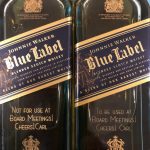
In most cases I’ve observed, the new Board members begin to understand over time why the other Board members and management have made the decisions they have made. Divergent director opinions gradually begin to converge. At the next Christmas after the proxy fight, I received an engraved bottle of Johnny Walker Blue scotch from Carl with the words, “NOT FOR USE AT BOARD MEETINGS”. At a subsequent Christmas, after our stock price had increased substantially, I received one that said, “TO BE USED AT BOARD MEETINGS”. Of course, I had to donate the bottles to charities or pay compensation to the company to avoid questionable receipt of a gift (Figure One)
For Mentor and Icahn Associates, the ending was good. The Icahn stock appreciated from a purchase price near $9 to a peak of over $25 and Icahn Associates more than doubled its investment when Mentor bought back half the stock at $18.50 and Icahn sold the rest. We discovered things about our financial and business structure that we might not have investigated if we had not been stimulated by our new Director demands. Although, two of the three Icahn Directors were not re-elected, the other one, David Schecter, was a strong contributor to the Board and we were sorry when he resigned.
The lesson for companies that come under attack? Continue to do what is best for your shareholders and resist acting in the interest of a minority shareholder just to reduce the pain of conflict. And keep an open mind; many of the themes that activists promote have merit even if they are driven by incomplete information. Ultimately, we all have the goal of increasing shareholder value and smart people working toward the same goal can usually find common ground.