At the SPIE Advanced Lithography Conference in February ASML gave an update on their EUV systems, in this blog I will provide a summary of what they presented. I have also written about my impressions on EUV for the overall conference here.
NXE3400B
The NXE3400B is ASML’s production EUV system shipping now and expected to be in production at multiple foundries late this year or early next year for 7nm processes.
The NXE3400B offers 13nm resolution to support 5nm logic and <15nm DRAM production. Full wafer critical dimension uniformity (CDU) is less than or equal to 1.1nm and machine to machine overlay (MMO) is less than or equal to 2.0nm with less than or equal to 60nm focus control. MMO from EUV to immersion systems is also around 2nm. Figure 1 summarizes the NXE3400B performance.
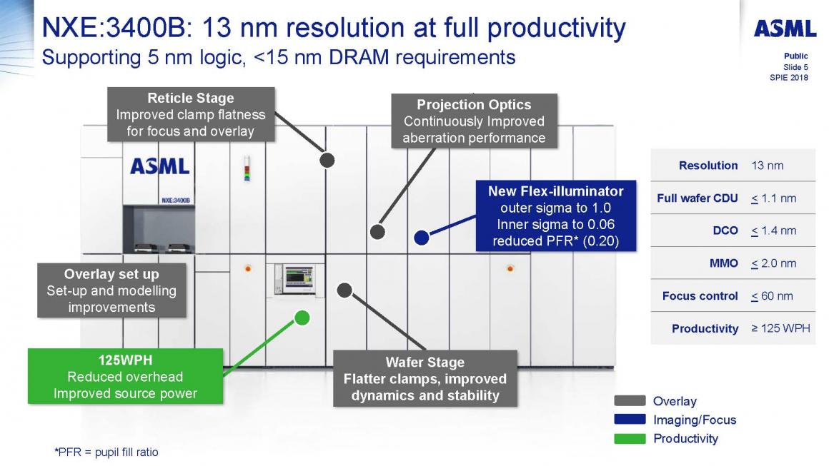
Figure 1. NXE3400B performance.
An EUV pellicle has now been demonstrated to support 245 watts with 0 defects greater than 10 microns. Work is underway to reach the high-volume manufacturing (HVM) target of 300 watts. Reticle transmission is currently 83% versus a 90% target. Authors note, EUV goes through the pellicle twice and the transmission has a significant impact on throughput, reaching 90% is highly desirable. Figure 2 summarizes the status of the EUV pellicle.
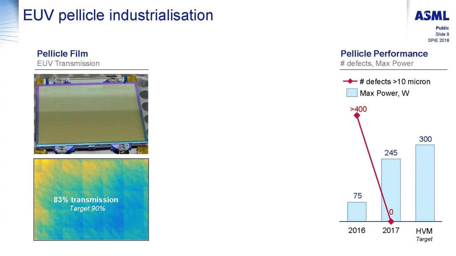
Figure 2. EUV pellicle status.
140 wafers per hour has now been demonstrated with a source running at 246 watts for 96 fields with a 20mJ/cm2 dose. The continued improvement in throughput is very good news because throughput will be a major challenge for HVM. Figure 3 presents the productivity trend for EUV systems.
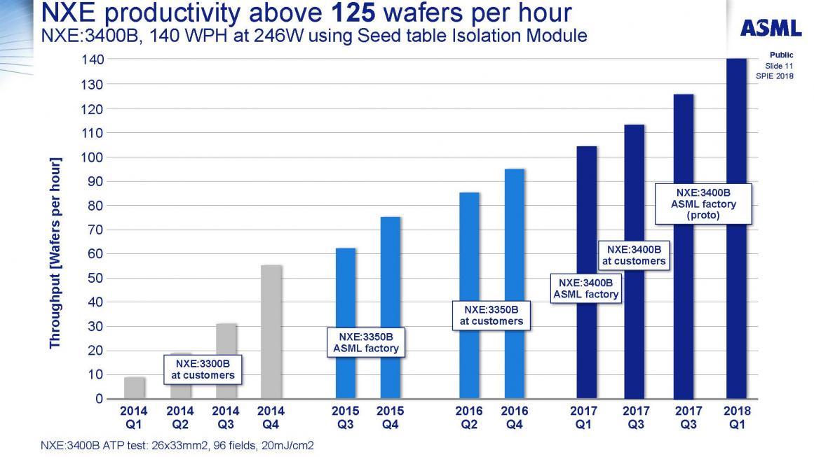
Figure 3. EUV system throughput.
The results in figure 3 are without a pellicle and at a 20mJ/cm2 dose. A pellicle may not be required for contacts and vias due to the low mask open area but will be required for metal layers reducing throughput. At least initially doses will likely be higher than 20mJ/cm2 also reducing throughput. For HVM continued improvements in throughputs will be highly desirable.
High-NA EUV lithography
Longer term High-Numerical Aperture (NA) EUV systems offer the ability to further improve resolution (R) with a single exposure.
The resolution of an optical system can be characterized by the Rayleigh criteria:
The NXE3400B system has an NA of 0.33, the new High-NA system will have an NA of 0.55 resulting in a roughly 2 node improvements in resolution.
High-NA improves contrast and therefore reduces local CDU. High-NA also reduces the need for multiple exposures and dose for LCDU improving throughput and should support 8nm resolution. High-NA does reduce depth of focus (DOF) as:
and will require tighter focus control.
A combination of high source power, increased optics transmission and a wider slit will result in 2-3x the power delivered to the wafer, this is achieved without increasing the power the pellicle is exposed. These improvements are expected to enable >185wph throughput. Figure 4 illustrates the delivered wafer power improvements.
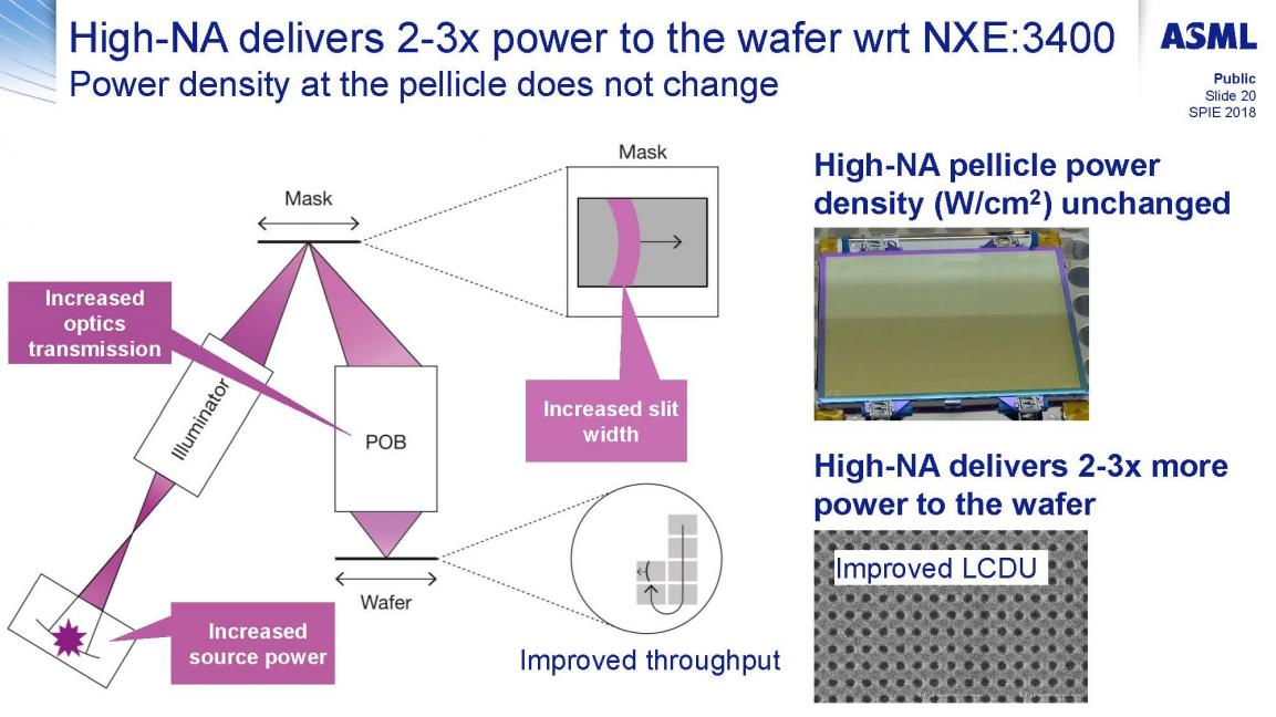
Figure 4. Power delivered to the wafer improvements.
High-NA EUV systems will require several system improvements:
- Mask stage acceleration will have to increase 4x.
- Wafer stage acceleration will have to increase 2x.
- A larger optical column is required.
- Wafer cooling.
The High-NA tools are significantly larger than current EUV systems and will require fabs with higher ceilings (see figure 5).
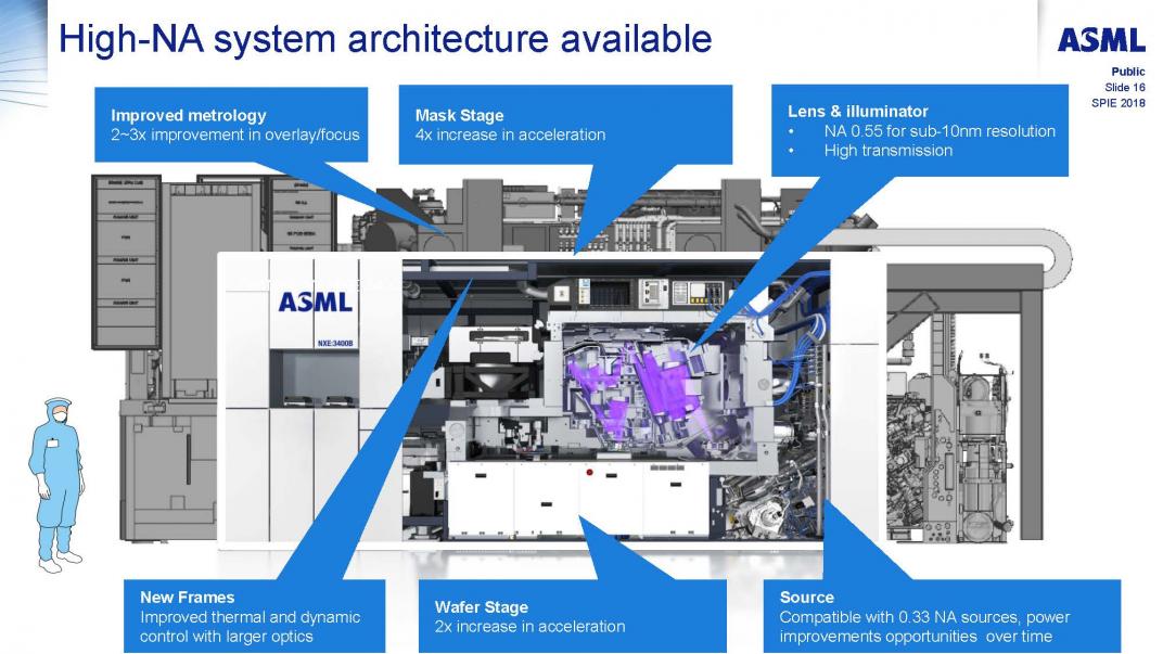
Figure 5, High-NA size relative to current EUV systems.
High-NA will use an anamorphic concept where the magnification is 4x on one axis and 8x on the other. This will limit the field size and may require stitching of fields to image a die. Work is continuing in this area.
There is a lot of work going into the system design to reduce particles and improve uptime. The system is also being designed to be modular to improve maintainability.
Zeiss is rapidly building out the capability to produce the required large-scale optics.
Conclusion
ASML continues to improve the current generation of EUV tools while building High-NA capabilities for the future. As I noted in my previous blog the conversation on EUV is evolving away from the system to stochastics and process implementation.


The Semiconductor Growth Numbers are Insane but the Real World Doesn’t Tally!