webinar banner AI 2026 v2

Semiconductor IP Security Issues

Semiconductor IP Security Issues
by Daniel Payne on 05-26-2019 at 4:46 pm

Accellera

Every morning I read the headlines from SemiWiki, CNN, LinkedIn and my Twitter feed, and it seems like every week that I read about another security breach that makes me wonder if anything online is secure. Companies try to harden their web sites, IT infrastructure and even their electronic products from being exploited or tampered with. Every article that you read about the IoT and connected devices is sure to mention security. Now let’s take the next step and say that you are designing a new SoC and intend to use hundreds of IP blocks, many from 3rd party vendors, so how do you know that each IP block will function properly and securely once integrated into a system?

I know that in the software world that we get new updates to improve the security of so many things, like: Operating Systems, desktop apps, mobile apps. Even my bike computer and cycling power meter have updates to fix bugs and make them more secure. Every semiconductor IP company has a process for making each IP block secure, but what about the entire industry?

Thankfully our industry has a well-known standards body, Accellera, and they have recently formed an IP Security Assurance Working Group.

Brent Sherman from Intel is the Chair, along with Mike Borza from Synopsys as the Vice Chair, so this looks like a solid start to tackle this concept of IP security across our semiconductor industry. You may even want to join this working group, so begin the process.

DAC 56 is coming up in June, so you should consider attending a luncheon and panel discussion on this timely topic of IP security assurance. The event is planned for Monday, June 3rd from Noon to 1:30PM in Room N246 in the Las Vegas Convention Center. It’s easy to register online here.

Accellera Chair Lu Dai will kick off the panel, and it should be lively and informative. The following speakers are panelists:

Brent Sherman, Intel
Lei Poo, Analog Devices
Serge Leef, DARPA
Andrew Dauman, Tortuga Logic
Adam Sherer, Cadence

I’ve worked at companies with both Serge Leef and Andrew Dauman, so these panelists are smart, experienced and articulate on the topic of IP security.

Summary

Exploitable vulnerabilities can be mitigated in semiconductor IP, so Accellera is forging ahead with an IP Security Assurance Working Group to create a standard that our industry can define and follow. Visit their web site and plan to attend the DAC luncheon and panel discussion to learn and participate.

Accellera

Accellera Systems Initiative is an independent, not-for profit organization dedicated to create, support, promote, and advance system-level design, modeling, and verification standards for use by the worldwide electronics industry. We are composed of a broad range of members that fully support the work of our technical committee to develop technology standards that are balanced, open, and benefit the worldwide electronics industry. Leading companies and semiconductor manufacturers around the world are using our electronic design automation (EDA) and intellectual property (IP) standards in a wide range of projects in numerous application areas to develop consumer, mobile, wireless, automotive, and other “smart” electronic devices. Through an ongoing partnership with the IEEE, standards and technical implementations developed by Accellera Systems Initiative are contributed to the IEEE for formal standardization and ongoing governance.


Automotive Design and Virtual Prototyping

Automotive Design and Virtual Prototyping
by Daniel Payne on 05-25-2019 at 5:40 pm

Synopsys Auto

The entire history of EDA software tools has enabled engineers to design ICs and SoCs using virtual prototyping, so most of us in the industry are familiar with the idea of modeling and simulating something as complex as an IC before actually starting the manufacturing process. In a complex system like an automobile there are a lot of sub-systems that use chips, software, firmware, operating systems, sensors, hydraulics, wiring and mechanical parts. Can engineers take the same virtual prototyping approach for multi-disciplinary projects like automotive?

Thankfully, the answer to that question is a resounding yes. In this blog I’m looking at what Synopsys has architected to meet the needs of the automotive market.

Virtual Hardware ECU

Electronic Control Units (ECU) are exploding in numbers, so a modern car can have 80+ ECUs in it, like: Engine Control Module, Powertrain Control Module, Transmission Control Module, Brake Control Module, Central Control Module, Central Timing Module, General Electronic Module, Body Control Module, Suspension Control Module (Source: WikiPedia). Synopsys has a virtual hardware ECU test bench approach that helps a team to integrate all of these ECUs, measure RAM and memory corruption, perform fault and coverage testing, automate regression testing and support the ISO 26262 functional safety standard.

Virtualizer Development Kits

Software developers can get an early start if only they had a model of the hardware, so that’s where Virtualizer Development Kits (VDK) come into play. You get to quickly assemble a virtual prototype by using pre-built virtual daughter boards. Even before your new MCU, SoC or ECU hardware has been fully designed, you can start developing software or porting an OS by using VDKs.

Center of Excellence

Creating an eco-system with automotive MCU and SoC vendors is essential for automotive virtual prototyping to grow, so Synopsys has created partnerships with the following IP and semiconductor companies:

ARM VDK Family for ARM Processors
Infineon VDKs for AURIX family
NXP VDKs for MPC5xxx Family
VDKs for S32
Automotive Platform
Renesas VDKs for  RH850 Family
VDK for R-CAR Family
ST Microelectronics VDKs for STELLAR Family
Synopsys VDKs for DesignWare ARC and EV Processor

Platform Architect MCO

Using a Transaction Level Model (TLM) to simulate your system design quickly is much preferred over low-level RTL code, plus there are much fewer lines of code. Even better, you can use a graphical system like Platform Architect MCO to partition hardware and software optimally for a multicore system.

Physical Prototyping

Automotive systems are highly complex with hardware, software and operating system interactions that take a massive amount of design and verification effort. To accelerate this challenge consider using physical prototyping like the Synopsys HAPS Prototyping product, it’s been proven over many years and will help your team speed up software development, improve hardware verification and system validation starting with just an IP block all the way up to processor subsystems and even a complete SoC.

Elektrobit

OK, using a virtual prototype sounds promising as a methodology, but who is actually using it so far in the automotive field? A company in Finland called Elektrobit has been providing automotive software for the past 30 years, and over 100 million vehicles depend on it for tasks like: connected car infrastructure, human machine interface (HMI) technology, navigation, driver assistance and ECUs.

Elektrobit used the VDKs from Synopsys to port their AUTOSAR operating system before silicon was ready. They also developed a concept virtual ECU that was based on the NXP Semiconductor S32 Automotive Processing Platform.

Summary

Automotive system design is becoming more complex with the electrification of vehicles and the approach of using virtual prototypes is certainly a big help in shortening design and verification times. Synopsys has invested heavily in this automation area and partnered with the leading IP and semiconductor companies to make virtual prototyping a best practice.

DAC 56 attendees will find Synopsys located in booth 367, which is in the back left-hand corner of the exhibit hall. I’ll be sure to stop by to learn more about their automotive offerings and meet my contacts.

Related Blogs


Silvaco Samsung and Excitement at 56thDAC

Silvaco Samsung and Excitement at 56thDAC
by Daniel Nenni on 05-25-2019 at 8:00 am

There were quite a few announcements at the Samsung Foundry Forum but my favorite was the IP partnership between Samsung and Silvaco. IP is a critical part of the fabless ecosystem and one of the advantages an IDM foundry has over a pure-play is the vast amounts of internal IP that have been silicon proven over the years. With Samsung being a leader in consumer electronics AND semiconductor manufacturing one could only imagine the types of IP that have passed through their fabs. Well imagine no more:

Samsung Foundry Begins Partnership with Silvaco to Launch their Semiconductor IP Assets

Targeted to consumer, mobile, IoT, automotive and AI/ML/HPC applications, the suite of design IPs includes wired and high-speed interfaces, analog and mixed-signal blocks and advanced security hard/soft cores.

Samsung Foundry IP

Wired and High-speed interfaces include: 

  • PCIe
  • DDR/LPDDR
  • MIPI PHY
  • Ethernet
  • HDMI
  • USB3.1 / DisplayPort
  • V-by-One

IP targeted to consumer applications include: 

  • Audio Codecs
  • Video Frontends
  • WiFi

High-performance and low-power analog IP include: 

  • PLLs
  • Integer
  • Fractional-N SSC
  • Low jitter
  • Data Converters
  • ADC
  • DAC
  • System Components

I have always said that EDA and IP go together like peanut butter and jelly. Silvaco has a very clever and highly scalable IP licensing model that came with the IP Extreme acquisition. Rather than compete head-to-head with the IP behemoths, which I highly discourage, Silvaco has changed the rules of IP engagement. The new Samsung relationship for example, where Silvaco will commercialize, market, distribute, customize, and support Samsung Foundry IP across multiple technology nodes. The Silvaco IP business model is highly collaborative with some of the top semiconductor companies around the world. The Samsung announcement is THE most disruptive IP announcement thus far this year and I expect more to come from Silvaco IP in the coming months, absolutely.

Silvaco DAC plan summarized:

  • Stars of IP party on Tuesday night at Topgolf. 
  • ClioSoft SOS7 is now integrated into Silvaco Analog Custom Design flow. 
  • Silicon Creations is using our ACD flow at 5nm.
  • We have new solution for IO characterization that 5X to 10X faster than existing solutions with no accuracy loss using our Viola + Jivaro tools.
  • PR to come regarding donation of the Silvaco 15nm Open Cell Library (a generic open-source, standard-cell library provided for the purposes of researching, testing, and exploring EDA flows) to SI2.
  • Here is our web-page that describes the Samsung IP: https://www.silvaco.com/products/IP/samsung_foundry_ip.html
  • Here is the Samsung press release:  https://www.silvaco.com/news/pressreleases/2019_05_13_01.html

DAC Theme: 
From Atoms to Systems: smart software solutions before and after manufacturing make all the difference. Stop by the Silvaco booth to learn more about our latest innovations: 

  • In partnership with Samsung Foundry, Silvaco now brings a suite of proven hard and soft IP to SoC engineers world-wide which include wired and high-speed interfaces, analog and mixed-signal blocks and advanced security functions.
  • New Viola™ I/O Pad Characterization solution saves days of simulation time.
  • Silvaco’s Analog Custom Design tool suite integrates ClioSoft’s SOS7 design management and multi-site team collaboration software for designers who use Silvaco’s Gateway™ schematic editor and Expert™ hierarchical IC layout editor to develop analog and mixed-signal designs for process nodes down to 7nm. This integration meets the demand by worldwide designs teams to create ICs and collaborate without risking productivity or data security.

We are showing the following products at DAC:

  • SIPware™ design IP for IoT, Mobile and Automotive ICs applications with hundreds of production-proven cores, including I3C, CAN-FD, and AMBA-based subsystems, plus the addition of new hard and soft IP from Samsung Foundry
  • Xena© for enterprise and cloud IP management with fingerprinting features for IP compliance
  • Gateway™Expert™Guardian™ for schematic driven physical layout with scripting and native DRC/LVS for designer productivity
  • Jivaro™Belledonne™ for optimization and analysis of extracted netlists and dramatic acceleration of SPICE simulation while maintaining accuracy
  • VarMan™ for high sigma analysis of analog blocks, standard cells libraries, memories with accelerated SPICE simulation, failure detection and accurate yield estimation
  • SmartSpice™SmartSpice Pro™ for fast circuit simulation of advanced nanometer-nodes
  • TechModeler™ for creating highly accurate behavioral Verilog-A compact simulation models of novel devices, from a small number of input samples
  • Cello™Viola™ for accelerated standard cell library creation and characterization of advanced FinFET nodes as well as mature technologies
  • Victory™ for 2D and 3D TCAD process and device simulation of nanometer CMOS, power devices, automotive applications and atomistic simulation of nano-meter scale devices such as quantum dots

About Silvaco, Inc.
Silvaco Inc. is a leading EDA tools and semiconductor IP provider used for process and device development for advanced semiconductors, power IC, display and memory design. For over 30 years, Silvaco has enabled its customers to develop next generation semiconductor products in the shortest time with reduced cost. We are a technology company outpacing the EDA industry by delivering innovative smart silicon solutions to meet the world’s ever-growing demand for mobile intelligent computing. The company is headquartered in Santa Clara, California and has a global presence with offices located in North America, Europe, Japan and Asia.


Monday DAC IP Session “PAM 4 Enable 112G SerDes”

Monday DAC IP Session “PAM 4 Enable 112G SerDes”
by Eric Esteve on 05-24-2019 at 1:00 pm

This session will open the DAC IP Track at 10:30 on Monday “How PAM4 and DSP Enable 112G SerDes Design” in Room N264. I am very proud to chair this invited paper session, as it addresses one of the key pieces of design, enabling to exchange data flow at the highest possible data rate. It can be between two chips on the same board, we talk about short reach (SR) or even in the same package with very short reach (VSR) or on a backplane, the interconnect is named long reach (LR). In any case, the goal is to send a high number of data through serial link(s) after serialization (Ser) and receive it via Deserialization (Des), so the SerDes acronym.

Initially used in telecom networking in the end of 1990’s, the SerDes was based on LVDS I/O running at 622 Mbps. At that time I was working with TI as ASIC Marketing in charge of telecom customers in Europe, and TI has made numerous design-win, thanks to this 622 Mbps LVDS SerDes. If we make a fast forward to 2008, an IP vendor like Snowbush was comfortable with PCI Express 2.0, based on 5.0 Gbps link, and was developing a 10 Gbps SerDes to support 10G Ethernet. In 2019, several IP vendors have developed silicon proven 112G SerDes. This is simply a 180-multiplication factor for the data rate in 20 years!

If you compare with the evolution of the CPU frequency, from about 1 GHz in 1998 to less than 5 GHz today, you realize the performance made by SerDes architects and designers. As usual in the industry, this evolution is the result of hard work made by multiple teams of mixed-signal designers. Nevertheless, it’s interesting to notice that, most often, innovation was supported by start-up. When the technology was proven and shipping, these start-ups were acquired, like V-semiconductor by Intel in 2012, Nusemi by Cadence in 2017 or Silabtech by Synopsys in 2018.

We have mentioned mixed-signal designers as SerDes design has been based on analog techniques since the beginning, even when equalization or pre-emphasis were used, and these are known to be signal processing related. But Digital signal processing (DSP) was too power hungry to be a viable solution. Up to the last FinFET nodes (7 nm and below), where pure DSP techniques could be successfully applied, as Tony Pialis, CEO of Alphawave, will show in his paper. If you want to understand the state-of-the-art in term of SerDes architecture, you will love this paper!

The invited paper from Rita Horner will explain you how 56G and 112G PAM 4 PHY can be used to build 400G or 800G Ethernet interconnects at every level in data center: intra rack, inter racks, room to room or regional. In all the papers, the move from NRZ to PAM 4 modulation type will be clearly described -it’s a good opportunity to learn from real experts.

If you are not convinced about the importance in the industry of SerDes based, very high speed PHY, just think about the incredibly growing demand for data bandwidth. The adoption of future applications is conditioned to a fast access to the cloud for an ever-increasing bunch of data. If you want your smartphone to benefit from 5G capability to download a video or run a specific application, you expect the wireless base station to scale, and move data to the data center as fast as possible. Industrial IoT, IoT and automotive applications will also require moving large amount of data to and from the data center, and inside this data center, as fast as possible.

SerDes based, very high speed PHY, is a small piece of design, initially 100% analog based, relying now on DSP techniques to reach 112 Gbps link speed. It’s also an essential piece of Silicon allowing supporting the 26% CAGR for Internet bandwidth (according with Cisco, see above picture). This move to PAM 4 PHY is the main enabler to support 112 Gbps, if you want to know more about it, come to the DAC IP session on Monday 3rd in Room N264.

From Eric Esteve from IPnest


400G Ethernet test chip tapes-out at 7nm from eSilicon

400G Ethernet test chip tapes-out at 7nm from eSilicon
by Tom Simon on 05-24-2019 at 10:00 am

Since the beginning of May eSilicon has announced the tape-out of three TSMC 7nm test chips. The first of these, a 7nm 400G Ethernet Gearbox/Retimer design, caught my eye and I followed up with Hugh Durdan, their vice president of strategy and products, to learn more about it. Rather than just respin their 56G SerDes, they decided to add the 112G SerDes, and at the same time use this vehicle for several other objectives. The gearbox in this chip contains 8 lanes of 56G and 4 lanes at 112G, allowing it to handle 400G Ethernet traffic. More than just showing that the SerDes work at 7nm, the configuration allows them to demonstrate a number of other things as well.

In our call, Hugh mentioned that they chose to work with Precise-ITC who develops IP for Ethernet and Optical Transport Network (OTN). They saw this as an opportunity to combine eSilicon interface IP with 3rd party IP to go through the process of integration and ensure that their StarDesigner 7nm flow was working as they expected. In essence this is a pipe cleaner of their SOC flow for 7nm.

Precise-ITC contributed a Forward Error Correction (FEC) block, Media Access Controller (MAC) and the Gearbox block. Having higher level functionality offers increased confidence in each element of the test chip. Hugh pointed out that this is a chip that customers can actually use as they evaluate the eSilicon’s offering. The chip will feature long reach and use only around 5W for the entire gearbox.

Designing at 7nm is even more difficult than at previous nodes. Lithography requirement impose many new restrictions on the layout. This makes designing chips with analog content challenging. Another aspect of the design that plays a critical role in the success of a chip like this is the packaging. Hugh told me that they used this opportunity to anticipate the complexity of designs with a much higher lane count by adding a more complex package design for some of the lanes. They also have the ability to inject noise during testing to ensure that the SerDes will perform in larger and more complex environments.

eSilicon is expecting to get silicon back in their lab by Q3 in 2019. They will make a test board that customers can use to put the SerDes and Ethernet related IP through its paces. The 112G SerDes will open the doors to continued development of Terabit Ethernet, which is becoming necessary with the explosion of data center throughput requirements.

eSilicon has consistently expended resources to stay at the leading edge of SOC technology. Their other May test chips included HBM and AI/ML designs all at 7nm. At the same time their partnerships will make life easier for their customers who are going to want to add advanced functionality to their designs. Test chips like this are a win for eSilicon, TSMC, Precise-ITC and their customers. We can eagerly await the return of silicon from this and their other test chips to learn more about how 7nm will perform in the wild. For more details, refer to the announcement on their website.


An evolution in FPGAs

An evolution in FPGAs
by Tom Simon on 05-24-2019 at 5:00 am

Why does it seem like current FPGA devices work very much like the original telephone systems with exchanges where workers connected calls using cords and plugs? Achronix thinks it is now time to jettison Switch Blocks and adopt a new approach. Their motivation is to improve the suitability of FPGAs to machine learning applications, which means giving them more ASIC-like performance characteristics. There is, however, more to this than just updating how data is moved around on the chip.

Achronix has identified three aspect of FPGAs that need to be improved to make them the preferred choice for implementing machine learning applications. Naturally, they will need to retain their hallmark flexibility and adaptability. The three architecture requirements for efficient data acceleration are compute performance, data movement and memory hierarchy. Achronix took a step back and looked at each element in order to recreate how programmable logic should work in the age of machine learning. Their new Speedster 7t is the result. Their goal was to break the historical bottlenecks that have reduced FPGA efficiency. They call the result FPGA+.

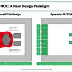
Built on TSMC’s 7nm node these new chips have several important innovations. Just as all our phone calls are now routed with packet technology, Achronix’s Speedster 7t will use a 2 dimensional arrayed network on chip (NoC) to move data between the compute elements, memories and interfaces. The NoC is made up of a grid of master and slave Network Access Points (NAPs). Each row/column operates at 256b @2.0Gbps, a combined 512 Gbps. This puts device level bandwidth in the range of 20Tbps.

The NoC supports specific connection modes for transactions (AXI), Ethernet packets, unpacketed data streams and NAP to NAP for FPGA internal connections. One benefit of this is that the NoC can be used to preload data into memory from PCIe without involving the processing core. Another advantage is that the network structure removes pressure during placement to position connected logic units near each other, which was a major source of congestion and floor planning headaches.

The NoC also allows the Achronix Speedster 7t to support 400G operation. Instead of having to run a 1000 bit bus at 724 MHz, the Speedster 7t can support 4 parallel 256 bit buses running at 506MHz to easily handle the throughput. This is especially useful when deep header inspection is required.

For peripheral interfaces, the approach that Achronix uses is to offer a highly scalable SerDes that can run from 1 to 112Gbps to support PCIe and Ethernet. They can include up to 72 of these per device. For Ethernet, they can run 4x 100Gbps or 8x 50Gbps. Lower rate Ethernet connections are also supported for back compatibility. They support PCIe Gen5, with up to 512 Gbps per port, with two ports per device.

The real advantage of their architecture becomes apparent when we look at the compute architecture. Rather than have separate DSPs LUTs and block memories, they have combined these into Machine Learning Processors (MLPs). This immediately frees up bandwidth on the FPGA routing. These three elements are used heavily together in machine learning applications, so combining them is a big advantage for their architecture.

AI and ML algorithms are all over the map on the need for mathematical precision. Sometimes large float precision is used, in other cases there has been a move to low precision integer. Google even has their own Bfloat precision. To handle this wide variety, Achronix has developed fracturable float and integer MACs. The support for multiple number formats provides high utilization of MAC resources. The MLPs also include 72Kbit RAM blocks, and memory and operand cascade capabilities.

For AI and ML applications, local memory is important, but so is system RAM. Achronix decided to use GDDR6 on their Speedster 7t family. It offers lower cost, easier and more flexible system design and extremely high bandwidth. Of course DDR4 can be used for less demanding storage needs as well. The use of GDDR6 allows each design to tune their memory needs, rather than being dependent on memory that is configured in the same package as the programmable device. Speedster 7t supports up to 8 devices with throughput of 4 Tbps.

There is a lot to digest in this announcement, it is worth looking over the whole thing. Looking back, this evolution will seem as obvious as how our old wired table top phones evolved into highly connected and integrated communications devices. The take-away is that this level of innovation will lead to unforeseen advances in end product capabilities. According to the Achronix Speedster 7t announcement, their design tools are ready now and they will have a development board ready in Q4.


Mentor Excitement at 56thDAC!

Mentor Excitement at 56thDAC!
by Daniel Nenni on 05-23-2019 at 10:00 am

Mentor continues to invest in conferences such as DAC, no matter the location, for which I am very grateful. They have a long list of activities this year but I wanted to point out my top three:

Wally Rhines has a talk in the DAC Pavilion which is first on the list. Wally’s expert industry perspective is the result of tireless research and endless customer meetings around the world and should not be missed. Wally will also be signing “From Wild West to Modern Life” books (last on the activity list) at the Mentor booth Monday at 5:00pm and Tuesday at 10:00am. There is a limited supply so I would get there early on either day. This is Wally’s first book, first book signing, and is your chance to get a piece of EDA history, absolutely.

FREE cappuccino from 9:00-2:00, and happy hour from 3:45-4:45 in the Mentor Booth. Hobnob with semiconductor professionals from around the world in the most casual setting. A great place to start and end your 56thDAC exhibition floor experience. I hope to see you there.

The 5G Myth vs. Reality Panel with Mentor, Synopsys and Cadence. Paul Mclellan and I were chatting about 5G at the Samsung Foundry event last week. His AT&T iPhone said he had a 5G connection while my Verizon iPhone said 4g. Identical phones different coverage. Marketing at its finest! This is an excellent opportunity to learn more about 5G from the semiconductor ecosystem, where electronics and 5G begins!

Activity List From Mentor Marketing:

The Design Automation Conference (DAC) is the premier conference for automated electronics design and verification technology. For 2019, DAC returns to sunny Las Vegas, Nevada at the Las Vegas Convention Center from June 2-5, 2019.

We’ve packed each day full of exciting activities and presentations featuring Mentor technical experts discussing the latest in cutting-edge design. You’ll find our experts in the conference program, in our booth (#334) hosting suite sessions and networking events, and in the Verification Academy booth (#617).

CONFERENCE PROGRAM

DAC Pavilion

Fundamental Shifts in the Electronics Ecosystem

MONDAY June 03, 10:30am – 11:15am | DAC Pavilion – Booth 871

Speaker: Wally Rhines – Mentor, a Siemens Business

Wally Rhines, CEO Emeritus of Mentor, a Siemens business, will examine major new market opportunities like AI/ML, automotive, 5G, etc. and how these markets will call for new design activity and the need for broader design tool innovation.  He will also explore whether we are heading into a period of stability after three years of disruption or if the revolution will continue.

Straight Talk with Tony Hemmelgarn, Siemens Digital Industries Software CEO

MONDAY June 03, 11:30am – 12:00pm | DAC Pavilion – Booth 871

Moderator: Ed Sperling

Myth vs. Reality: What 5G is Supposed to Be, And What it Will Take To Get There

TUESDAY June 04, 11:30am – 12:00pm | DAC Pavilion – Booth 871

5G is trumpeted as the big enabler, providing massive throughput and a massive upgrade path for the mobile and mobility markets. It is a way for cars, phones and other connected devices to stream massive amounts of data to the cloud and back again. But 5G signals don’t travel very far, and they don’t penetrate objects. Devices built for this market will require extreme power management so they aren’t searching for signals constantly. Parts of them will always be on, which has an impact on design and reliability. And some parts, such as the antenna arrays, cannot even be tested using conventional means.

Panelists:

Neill Mullinger – Mentor, a Siemens Business

Peter Zhang – Synopsys

Ian Dennison – Cadence Design Systems

Paper Presentations

MONDAY, June 03

4.4 Electromigration Signoff based on IR-drop Degradation Assessment

8.4 Local Layout Effect Aware Design Methodology for Performance Boost below 10nm FinFET Technology

TUESDAY, June 04

18.4 A Lightweight Hardware Architecture for IoT Encryption Algorithm

WEDESNDAY, June 05

66.4 Virtual Methodology For Performance and Power Analysis of AI/ML SoC Using Emulation

69.4 Efficient Verification of High-level Synthesis IP

Posters

123.21 Metric Driven Power Regression – A Methodology based Metric Driven Approach for Power Regressions

123.25 River Fishing: Leverage Simulation Coverage to Drive Formal Bug Hunting

124.2 Comprehensive Analog Layout Constraint Verification for Matching Devices

124.7 Enabling Exhaustive Reset Verification in Intel Design

124.16 A Smart RTL Linting Tool with Auto-correction

124.25 Configurable Multi-protocol AUTOSAR-based Secure Communication Accelerator

125.12 Faster PV Signoff Convergence in P&R using RTD

125.14 Hybrid Methodology- An Innovative Methodology for Hierarchical CDC Verification

Moving Up in the World

125.17 Functional Safety on A-R-M CPUs

125.21 Tackling the Increasing Challenge of IR drop & EM Fails in Advanced Technologies with a Push Button Solution

EXHIBIT FLOOR

Mentor’s booth #334 is located on the west end of the exhibit floor. Check in daily for a host of technical sessions, networking events, panel discussions, a free cappuccino from 9:00-2:00, and happy hour from 3:45-4:45! You’ll also find Mentor verification experts in the Verification Academy booth (#617) for in-depth sessions on Portable Stimulus, UVM, and more.

Technical Sessions in the Mentor Booth

Each day, Mentor experts will be in the booth delivering technical sessions across:

  • AMS Verification
  • Analog/Mixed-Signal Verification
  • Design & functional Verification
  • Digital Design & Implementation
  • IC Design & Test

You can view the complete list of technical sessions and pre-register here.

Expert Panel Discussions

Mentor experts will be moderating in-booth panels on both Monday and Tuesday directly following happy hour. Make sure to pick up a free glass of wine or beer before!

Design Smarter Innovations Faster using AI/ML and More with Mentor, a Siemens Business

MONDAY June 03, 4:00pm – 4:45pm | Mentor Booth #334

To enable our customers to deliver smarter innovations to market faster, Mentor, a Siemens business is actively delivering new solutions and use models that enable our customers to more readily develop AI-powered technologies. We are also integrating advanced machine learning algorithms into our existing tools to enable those tools to deliver better results faster. Come hear experts from across Mentor’s IC solutions portfolio describe what Mentor has to help customers deliver smarter IC innovations to market faster.

Panelists:

Ellie Burns, director of marketing, Calypto Systems Division

Vijay Chobisa, product marketing director, Mentor Emulation Division

Geir Eide, product marketing director, D2S Tessent Division

Amit Gupta, general manager, Solido, IC Verification Solutions Division

Steffen Schulz, vice president product management, D2S Calibre Marketing

Functional Safety in Isolation – Can Safety Be Collaborative?

TUESDAY June 04, 4:00pm – 4:45pm | Mentor Booth #334

As companies strive for greater levels of autonomy, more capability will be required of automotive ICs living at the edge, and the challenge of ensuring functional safety is exacerbated. The mass public trusts companies to deliver safe products to the market, but can the industry deliver on that promise given the demand for rapid innovation and complexity within the automotive ecosystem and supply chain? The scope of functional safety extends beyond the product boundaries to systems of interlinked devices representing the complete transportation network. From IP to automobile, each product plays a role in the overall functional safety of the transportation network. New paradigms and methodologies are required to ensure functional safety across all levels of the automotive ecosystem.

Panelists:

Yves Renard, Functional Safety Manager, ON Semi

Ghani Kanawati, Technical Directory of Functional Safety, Arm

Matt Blazy-winning, Functional Safety Director, NXP

Book Signing with Wally Rhines

Wally Rhines will be at the Mentor booth signing copies of his new book, “From Wild West to Modern Life”, Monday at 5:00pm and Tuesday at 10:00am.



Mentor Extends AI Footprint

Mentor Extends AI Footprint
by Bernard Murphy on 05-23-2019 at 8:00 am

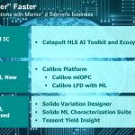
Mentor are stepping up their game in AI/ML. They already had a well-established start through the Solido acquisition in Variation Designer and the ML Characterization Suite, and through Tessent Yield Insight. They have also made progress in prior releases towards supporting design for ML accelerators using Catapult HLS. Now they’ve stepped up to better round out (in my view) Catapult support, also to introduce new ML-enabled capabilities in Calibre.

Joe Sawicki (who needs no introduction but for completeness is EVP of IC EDA at Mentor/Siemens) kicked off this announcement with some background on AI/ML, starting with a nice infographic on startups in AI (over 2000 with $27B in funding) and the AI chip landscape, estimated to be $195B by 2027. Will all or even most of the startups make it? Of course not – startups have a significant fallout rate in any field. But the practical stuff – computer vision, keyword/phrase recognition, localization and mapping for robots, among others – this is real, and has massive potential in many markets. Siemens particularly is very interested in the Industry 4.0 opportunities. Joe also noted that over half the fabless venture funding since 2012 has gone into AI startups, most of it relatively recently, which is even more impressive.

Joe sees challenges in this area in four domains: optimizing ML accelerator architectures, managing power, dealing with huge designs (up to reticle size) and dealing with high speed I/O for fast memory access and communication. This is driven in part by winner-take-all competition in these application domains, demanding differentiation in hardware architecture towards application-specific goals at the edge versus ultimate performance in data-centers (DCs). Edge nodes need ultra-low power for long battery life and DCs still need manageable power (no-one wants to scale-out power hogs). Performance requirements in DC ML accelerators demand deeply intermixed logic with multiple levels of embedded memory, driving massive die sizes and need for fast access to off-die working memory through interfaces such as HBM2 and GDDR6.

For Joe, this maps onto design needs in top-down optimization through HLS, higher capacity and faster, scalable tools everywhere (he noted particularly that he sees this domain driving huge growth in emulation, particularly for power verification), power budget management and need for a flexible AMS flow, especially at the edge where you need to optimize from sensors straight into inference engines (aka smart sensors).

Ellie Burns (Mktg Dir for digital design implementation solutions) followed to describe progress the have made in Catapult HLS for AI/ML design. I first wrote about what they are doing in this area about a year ago. The value proposition is pretty clear. HLS works well with neural net architectures, ML designers for edge applications want to functionally differentiate while also squeezing PPA as hard as they can (especially power, for e.g. wake-words/phrases), so fast analysis and verification through the HLS cycle is a great fit.

The Catapult team have been working with customers such as Chips and Media for a while, optimizing the architecture and flow and they now have an updated release, including (again in my view) some important advances. First, they now have a direct link to TensorFlow. Earlier you had to figure out yourself how to map a trained network (trained almost certainly on TensorFlow) to your Catapult input; do-able but not for the timid. Now that’s automated – big step forward. Second, they now have HLS toolkits for four working AI applications. And finally, they provide an FPGA demonstrator kit compatible with a Xilinx Ultrascale board. You can checkout and adapt the reference design and prove out your ML recognition changes from an HDMI camera through to an HDMI display. The kit provides scripts to build and download your design to the board; board and Xilinx IP such as HDMI are not included.

Steffen Schulze (VP Calibre product management) followed to share the latest ML-driven release info for Calibre OPC and Calibre LFD. Almost anything in implementation is for me a natural for ML – analysis, optimization, accelerated time to closure – all good candidates for improvement through learning. Steffen said they have done a lot of infrastructure work under the Calibre hood, including adding APIs for the ML engine, seeing potential for other applications to also leverage this new capability.

On ML-enabled OPC, Steffen first presented an interesting trend graph – the predicted number of cores required to maintain a similar OPC turn-around-time versus feature size. The example he cites is for critical layer OPC on a 100mm2 die using EUV and multiple patterning, starts at around 10k cores for 7nm and trends more or less linearly to around 50k cores at 2nm.

He said that, as always, scalability of the tools helps but customers are looking for more performance and increased accuracy through algorithmic advances to cope with these significantly diffraction-challenged feature-sizes. As an interesting example of real-world application of ML in a critical application, they use the current OPC model to drive training, then in application to the real design they use one ML (inference) pass to get close followed by two traditional OPC passes to resolve inconsistencies and problems with unexpected configurations (configs not encountered in the training I assume). This approach is delivering 3X runtime reduction and better yet, improved edge placement error (a key metric in OPC accuracy).

For Calibre LFD (lithography-friendly design), let me start with a quick explanation since I’m certainly no expert in this area. The dummies guide, at least as this dummy understands it, is that processes and process variability today are so complex that the full range of possibly yield-limiting constructions can no longer be completely captured in design rule decks. The details that fall outside the scope of DRC rules require simulation to model potential differences between as-drawn and as-built lithographies. The purpose of Calibre LFD is to do that analysis, based on an LFD kit supplied by the foundry.

The ML-based flow here is fairly similar, starting with labeled training followed by inference on target designs. The training is designed to identify high-risk layout patterns, passing only these through for detailed simulation. This delivers 10-20X improvement in performance over full-chip simulation. Steffen also said that using this approach they have been able to find yield limiters that were not previously detected. Here also, ML delivers greatly increased throughput and higher accuracy.

To learn more about what Mentor is doing in AI/ML in Catapult and Calibre, see them at DAC or click HERE and HERE.


Webinar Recap: IP Life Cycle Management and Traceability

Webinar Recap: IP Life Cycle Management and Traceability
by Daniel Payne on 05-22-2019 at 10:00 am

Earlier this month I attended a webinar organized by Methodics on the topic of IP life cycle management and traceability, with three presenters and a Q&A session at the end. I’ve worked with Michael Munsey before and he was the first presenter. Semiconductor IP creation and re-use is the foundation of all modern IC designs, and keeping track of hundreds to thousands of IP blocks along with design scripts and verification results becomes a complicated process very quickly, especially if you’re still using a manual approach.

Methodics provides products in three major areas:

  • IP Lifecycle Management – percipient, versic
  • Enterprise Data Storage Acceleration – warpstor
  • Scaleable, Massively Parallel Job Execution – arrow

This webinar was focused on IP Lifecycle Management, aka IPLM. The company has been around since 2006, has an HQ in SFO, and is staffed with 32 professionals in the USA, Europe and Pacific Rim. Their tools work with popular vendors, like: Perforce, Siemens, Cadence, Synopsys, Jama and neo4j.

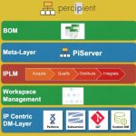
The percipient tool has five layers of abstraction, as shown below, where engineers have in a single place to access all of the information about their IC design and can track release management and versions.

Rien Gahlsdorf then gave us a live demo of percipient showing multiple ways to use the tool: command line, web, Cadence, API. Percipient is built on top of a DM system, then manages both meta-data and releases. Users can recall all IPs for any release made earlier, manage all file types, manage IP hierarchy, attach meta data to an IP, view layout, view schematics, review the design state. Making a new release can automatically trigger scripts: Simulations run, requirements checked.

percipient

Michael talked about functional safety (FuSa) and the challenges of complying with the ISO 26262 standard where traceability is a requirement from specification to design, verification and release.

The Methodics approach has a link from requirements through design and verification, enabling compliance with the ISO 26262 standard. Rien demonstrated a second time showing requirements in jama, making a release with Perforce, checking in IP with the latest version, and how a release can trigger scripts to run.

To make ISO 26262 compliance easier the percipient tool comes with IP templates that are configured with properties and attributes. There are survey and doc templates that automate the collection and FuSa interview responses.

In the final demo Rien showed how the percipient tool helps capture all meta-data throughout the entire design process, and automates release management. Documentation is even automated with percipient, where each IP gets a chapter in the design documentation, along with all meta-data entered, hyperlinks added and property values shown.

Q&A

Q: There are other traceability products, like from IBM, so why percipient?

A: percipient allows management of IP, traceability, FuSa compliance, etc. We know how to build a design BOM. Verification, design and requirements are all traceable. This was built from the ground up to achieve this.

Q: Is it possible to capture document and code reviews?

A: Usually within GIT you would use that code review feature, natively.

Q: How do you track a family of data?

A: In the demo we showed data types, there are no restrictions, you can have tables, graphs, charts, families of related data, hierarchical tables.

Q: is percipient DM agnostic?

A: Yes, we work with all the popular DM tools, plus we offercustom support as well. GIT, Perforce, Sharepoint, etc.

Summary

The percipient tool enables traceability from Design to Release to Verification. No more manual, error-prone engineering practices.

To view the webinar video archive visit here.

Related Blogs


What are SOTIF and Fail-Operational and Does This Affect You?

What are SOTIF and Fail-Operational and Does This Affect You?
by Bernard Murphy on 05-22-2019 at 7:00 am

Standards committees, the military and governmental organizations are drawn to acronyms as moths are drawn to a flame, though few of them seem overly concerned with the elegance or memorability of these handles. One such example is SOTIF – Safety of the Intended Function – more formally known as ISO/PAS 21448. This is a follow-on to the more familiar ISO 26262. While 26262 provides processes and definitions for safety standards of the hardware in electrical and electronic systems in automobiles, it has little to say about the high-levels of automation that dominate debate around autonomous and semi-autonomous cars.


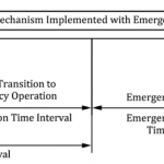
ISO 26262:2018 introduces the Emergency Operation Time Tolerance Interval to account for fail operational use cases

Safety at SAE level 2 and above automation is no longer simply a function of the safety of the hardware. When systems-on-chip are running complex software stacks, quite often multiple stacks, and those systems use probabilistic AI accelerators depending not only on software but also on arrays of trained weights, then there’s a lot more that can go wrong beyond the transient faults of 26262.

An SoC designer might assert “Yes these are problems, but they have nothing to do with my hardware. My responsibilities stop at ensuring that I meet the ISO 26262 requirements. All the rest is the responsibility of the system and software developers.” But you’d be wrong, based on where SOTIF is heading. High levels of integration and non-deterministic compute elements (AI) in safety-critical applications raise a new question; how should the system respond when something goes wrong? And how do you test for this? Because inevitably something will go wrong.

When you’re zipping down a busy freeway at 70mph and a safety-critical function misbehaves, traditional corrective actions (e.g., reset the SoC) are far too clumsy and may even compound the danger. You need something the industry calls “fail operational”, an architecture in which the consequences of a failure can be safely mitigated, possibly with somewhat degraded support in a fallback state, allowing for the car to get to the side of the road and/or for the failing system to be restored to a working state. According to Kurt Shuler (Arteris VP of marketing and an ISO 26262 working group member), a good explanation of this concept is covered in ISO 26262:2018 Part 10 (chapter 12, clauses 12.1 to 12.3). The system-level details of how the car should handle failures of this type are decided by the auto OEMs (and perhaps tier 1s) and the consequences can reach all the way down into SoC design. Importantly, there are capabilities at the SoC-level that can be implemented to help enable fail operational.

Redundancy engineering is becoming more important in SoC functional safety mechanism design. In safety-critical areas in the design, you use two or more versions in parallel and compare the outputs. This is called static redundancy and sounds suspiciously like the TMR, lockstep computing and similar safety mechanisms you already use for ISO 26262. And to some extent they are. But as I understand it, there are a couple of key differences. First these requirements are likely to come from the OEM (or Tier 1), over and above anything you plan to add for redundancy. And second, in a number of redundancy configurations (called dynamic redundancy), these independent systems are expected to self-check their correctness. For example, there is a redundancy style called “1 out of 2 with diagnostics” (1oo2d) in which perhaps 2 cores would each compute a result in parallel, and also each provide a self-check diagnostic. The comparison step can then feed-forward a fail-operational result if both cores self-check positively and agree, or if one core self-checks positively and the other does not.

Another major component of fail-operational support requires the ability to selectively reset/reboot subsystems in the SoC. A very realistic example in this context would be for a smart sensor SoC containing (among many subsystems) one or more vision subsystems (ISPs) and one or more machine learning (ML) subsystems. On a failure in one of these subsystems, rebooting selectively allows other object-recognition paths to continue working. This obviously requires a method to isolate individual subsystems so that the rest of the system can be insulated from anomalous behavior as the misbehaving subsystem resets. One SoC network-on-chip interconnect company, Arteris IP, is already pioneering technology to enable this.

Redundancy in ML subsystems as described above allows for one class of failures in recognition, but what about failures resulting from training problems? One idea that has been suggested (though I don’t know if anyone has put it into practice) is to use asymmetric redundancy between two ML system trained on different training sets. It will be interesting to see how that debate evolves.

The system interconnect is the ideal place to manage a lot of this functionality in the SoC, from “M out of N” redundancy (maybe with diagnostics) to isolation for selective reset/reboot. Arteris IP have made significant and well-respected investments in this area. You should check them out.