Solving critical customer problems sometimes isn’t enough. One of my most interesting experiences came during the development and rollout of a product that was designed to optimize integration of hardware and embedded software. In this case, the product performed exactly as planned but the plan ignored the organizational complexities that come with specialization of skills in different divisions of a large company.
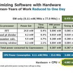
The product, called ASAP (not a great name but that wasn’t the reason it failed), analyzed a customer’s design at the RTL functional level, along with the embedded software. It determined where the bottlenecks existed for optimum performance or power of the system. We found an ideal customer who was designing a portable consumer product that was dissipating 8.5 Watts and wasn’t viable with the required size of batteries. Three engineers had worked for a year trying to reduce the power and had modified the design to dissipate only 6.5 watts, still far from the required 4.5 watts. We analyzed the customer’s design and, within a few hours, generated changes that reduced the power to 4.1 watts, well below the 4.5 watts goal of the customer. This was done by identifying bottlenecks and automatically synthesizing hardware to substitute for functions that were inefficiently executing in software on an embedded CPU (Figure 1). The customer was ecstatic about the result and we expected a major sale.
Figure 1 – Automatic analysis and synthesis to achieve reduced power
When we didn’t receive an order, we investigated. The problem, it turned out, was an internal disagreement. While the customer engineers agreed that they badly needed our product, they couldn’t agree which group, hardware or software design, would be responsible for using it. The hardware engineers were adamant that “no software engineer is going to generate hardware in my chip design” and the software engineers were adamant that “no hardware engineer is going to change a single line of my software”. Amazingly, the disagreement was so strong that they decided not to adopt our product and, instead, to kill the development of their own very promising product.
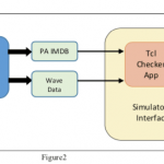
You might think that this was an extreme example but I’m increasingly convinced that it wasn’t. We experienced the same thing every time we developed products that crossed domains of expertise, from analog to digital, from mechanical to electrical, from software to hardware, from design to manufacturing, etc. Software tools that appealed to one domain were not accepted by the other domain. (Figures 2 and 3)
Figure 2. Differences in the way specialized groups do their work make it difficult to provide tools that cross domain boundaries
Figure 3. Differing standards, metrics of performance, modes of communication and other differences prevent system level optimization
This is a phenomenon that appears repeatedly, especially in large organizations. There are, however, ways that system level optimization can be achieved. Some of these are listed in Figure 4. One of the most apparent examples of the evolution from problematic partitions to a successful organization structure was the change in the customer/supplier relationship that evolved with the advent of silicon foundries in the semiconductor industry over the last thirty years. When most semiconductor companies were vertically integrated, the tradeoffs of every new process technology led to major feuds between the design and the manufacturing engineers. I know this because I had to referee the arguments many times. A new generation of product required the most aggressive feature sizes possible while manufacturing yield and throughput favored the least aggressive. A compromise had to be made and it usually was influenced more by politics than by engineering. With the emergence of silicon foundries, the problem went away. Now there were suppliers whose success depended upon providing the most aggressive design rules possible in a cost-effective manufacturing environment. No more politics. Just an insightful analysis of the manufacturing and design tradeoffs.
Another approach to solving the specialization problem is to form a startup company (Figures 4 & 5). In a typical early stage startup, partitions of specialization have not yet formed, so the hardware engineer also frequently writes some of the embedded software, or is at least heavily involved in both. In addition, startups typically have a key technical expert who will be respected by the potential customers’ most valuable development engineers. The two of them can get together and exchange ideas for the ideal product because the startup engineer is not constrained by finding the solution in only one domain, e.g. in software or hardware.
Assimilating the task of one group into another also removes artificial partitions. This assumes that the new group truly integrates the responsibilities. It could mean making a group leader at a low level responsible for an integrated solution that involves both hardware and software, for example.
Figure 4. Ways to overcome the barriers of organizational partitions
Figure 5. Removing the interfaces between customer and supplier
Another approach is to move the design to a higher level of abstraction so that tradeoffs can be made among differing specialties, e.g hardware/software, mechanical/electrical, etc. If the abstraction level is high enough, then everyone can speak the same language (Figure 6).
Figure 6. Abstraction temporarily solves optimization challenges
This works for a while but very quickly, the addition of detail into the design causes a split among specialties and the optimization effort is reduced or ceases entirely. In some industries, a new abstraction layer can be created at a lower level to overcome this problem. SysML is one example. AUTOSAR, for the automotive industry, is another.
Another solution is to conduct multi-physics simulation of designs to see the impact of tradeoffs in different domains (Figure 7). Even with this type of simulation data, it’s frequently difficult to determine which design domain should make changes to improve system level performance. As a minimum, however, it provides data for a rational discussion and takes some of the emotion out of the decisions.
Figure 7. Multi-physics simulation
While these approaches offer potential, one must wonder whether there are any solutions that are universally applicable? One overarching approach comes from the way a company handles its data management. For years, company managements hoped for the universal workstation that could be used by the many different disciplines— mechanical, electrical, software, etc. That is not likely to happen. Engineers need their own ways of working with design and manufacturing data and they are not going to change, nor would it be advisable to do so. Efficiency in one domain requires different tools and methods of analyzing data that may not be efficient in another domain.
Despite this need for separation of development functions, engineers still need information from other domains to do their jobs. A systems company needs a centralized database from which groups in different areas of the company can download and upload data for their own work and to access information from other domains. A good example is the engineer who is developing wiring for a plane or car. Electrical design of the wiring harness requires detailed electrical simulation, analysis of potential sneak paths and optimization of “take up” alternatives of options in the vehicle so that the basic wiring cost is minimized while the wiring harness can be customized for a multiplicity of option combinations in a vehicle. At the same time, the wiring approach will change to meet the three-dimensional characteristics of the mechanical design of the vehicle. How does the electrical designer obtain the data needed to determine if a wire bundle will fit through a hole in the frame of the car? Or how does the designer know the wire lengths in three dimensions? Does the designer import the mechanical database? Impractical and probably impossible. An extract of estimated wire tracks and lengths must be exported to the mechanical design environment and then simulated with mechanical models and tools. Similarly, subsets of system design data must be extracted from one design discipline to another throughout the design process evolution.
Figure 8. In an enterprise data base, unique data structures are needed for each type of discipline
Over many years, I have had the opportunity to work with teams to develop and modify products to make them usable by developers in different domains of expertise. Some of the lessons learned from this experience are illustrated here.
First, it’s important to provide unique data structures and dataases for each discipline. Mentor’s experience with Version 8.0 of our software drove this one home. Forcing all the users to format their data in a fixed set of predetermined formats creates an inflexible system that doesn’t benefit anyone but the database vendor. The database needs to be open and flexible. Beyond Mentor’s own disastrous experience with the fixed data formats of the Falcon 8.0 database, we were later forced to support our Capital electrical architecture software on a Catia set of formats that suffered the same problem as Falcon. Performance would have been hopelessly compromised, changes to database structures would require a major regeneration and verification of the database software and our product would have been vulnerable to knockoff by the database owner. Instead, we created a digital flow for our data outside the Catia database. This approach requires working with data base vendors who favor openness. This has always been a fundamental priority for Siemens Teamcenter and federated data base approaches of other companies but not necessarily for all database providers. Openness was a key compatibility philosophy for the merger of Siemens with Mentor Graphics that made the union successful.
Figure 9. Don’t burden one discipline with another discipline’s detailed information
As mentioned earlier, there are still many people who believe that disparate design disciplines in a company should all use the same workstations, the same user interface, the same data structures, etc. This philosophy is driven by the idea that it is good to have a single design and verification environment that transcends the differences in the enterprise. Engineers can then move from group to group with minimal retraining and design information is more easily shared. Despite support for this concept among the managements of many companies, it rarely, if ever, happens. Burdening an electrical designer with the overhead of the mechanical, manufacturing, thermal, etc. detailed design information doesn’t seem to work. The trick is to be able to access the pieces of data from another domain that are needed to do your job in your domain. Even better is an architecture that lets you export abstractions of your design to another domain to perform tasks not well suited to the domain of your expertise. This is how electrical wiring is done when the electrical designer needs to make sure his design meets the constraints of the mechanical embodiment of the product (Figure 10).
Figure 10. Enable selective access to the required data; facilitate rapid translation of data formats
Flexibility and openness of the enterprise data base is the most important criterion (Figure 11). If addition of a new data format requires a major revision of the entire data base system, it’s impractical to wait. Typically, other things are impacted when a major revision of this type is attempted so the data base structure must be designed for flexibility to change some formats without having to reverify the entire database system.
Finally, the more a design environment feels familiar, the more likely the development engineers will create good products (Figure 12)
Figure 11. Make sure the enterprise data management has the flexibility to add or change data formats selectively without re-verification of the entire data base management system
Figure 12. Developers have enough to worry about without adapting to changes in their design environment and support
Although the “lessons learned” provide guidance for how data bases and design environments should be structured, few large corporations have been able to implement the level of interoperability between disciplines that they would like. Figure 13 is still a hope rather than a reality. Even if the commercial databases and design software provide the capability for data to be accessed and analyzed from functional domain to functional domain, system optimization would still require that compromises be made in one domain to achieve the optimum result at the system level. Perhaps this is why systems companies who find ways to overcome this challenge have traditionally achieved higher operating margins than component companies.
Figure 13. Specialization in large enterprises can be a strength, rather than a burden. Development environments that maintain the needed specialization by discipline while affording access to data in other domains leads to the most productive enterprise
It’s likely that success will evolve application by application. The case of electrical wiring of cars and planes reached such a critical level that integrated solutions evolved among the electrical, mechanical and manufacturing domains. Other applications are reaching a critical point where system optimization can only be achieved in an environment where multi-domain tradeoffs can be made. Making these tradeoffs at the highest possible level of abstraction is most likely to produce an optimum result and is also most likely to facilitate compatible development in the diverse functional domains of the corporation.