You are currently viewing SemiWiki as a guest which gives you limited access to the site. To view blog comments and experience other SemiWiki features you must be a registered member. Registration is fast, simple, and absolutely free so please, join our community today!
If you follow my blogs you know that Arteris IP is very active in these areas, leveraging their central value in network-on-chip (NoC) architectures. Kurt Shuler has put together a front-to-back white-paper to walk you through the essentials of AI, particularly machine learning (ML) and its application for example in cars.
He also highlights an interesting point about this rapidly evolving technology. As we build automation from the edge to the fog to the cloud, functionality, including AI, remains quite fluid between levels. Kurt points out that this is somewhat mirrored in SoC design. In both cases architecture is constrained by need to optimize performance and minimize power across the system through intelligent bandwidth allocation and data locality. And for safety-critical applications, design and verification for safety around intelligent features must be checked not only within and between SoCs in the car but also beyond, for example in V2x communication between cars and other traffic infrastructure.
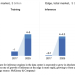
What’s driving the boom in AI-centric design? If you’re not in the field it might seem that AI is just another shiny toy for marketing, destined for the garbage can when some inevitable fatal flaw emerges. You couldn’t be more wrong (pace Sheldon Cooper). Tractica estimates that more than 80% of the growth in semiconductors between now and 2025 with be driven by AI applications, whether based on standard platforms (CPU, GPU or FPGA) or custom-built ASIC/ASSPs or highly-specialized accelerators. (The overlay in the image above is Kurt’s addition).
None of this demand depends on major inflection points in the way we live. It’s all about incremental improvements to safety, productivity, security, convenience – all the things technology has been improving for a long time. Whether or not ADAS in cars impresses insurance providers (per my earlier blog), it definitely impresses this owner and apparently many others. I’ve said before I’ll never switch back to a car with lesser ADAS features – they more than pay for themselves. Security for business and industrial plants is already moving from need to constantly monitor security camera feeds to only having to check when unusual movement and/or sounds (dog barking, glass breaking) are detected. Also incidentally this is much better for home security.
Oncologists may be able to more reliably detect potentially cancerous lung tissue based on CT scans (following further analysis). Smart storage solution providers now need to build intelligence into their solutions to better manage housekeeping and other scheduling to maximize throughput and minimize failures. All of this is bread-and-butter stuff, no consumer, industrial or business revolutions required, just adding more automation to what we already have.
McKinsey went a step further than Tractica, breaking down AI hardware growth between training and inference in the datacenter and training and inference on the edge. The biggest contributors are in the datacenter (I’m curious to know how much of that is for cat recognition and friend-tagging in Facebook photos.) And the highest growth is on the edge, growing in 7 years from essentially zero to $5-6B. These two surveys don’t come up with the same numbers for 2025, but that’s not very surprising. What is consistent is the high growth.
Why do Kurt and Arteris IP care about this? They care because the interconnect within an SoC is proving to be at the nexus of AI performance, power, cost and safety for these fast-growing applications. On performance, power and cost, these are big SoCs, smartphone AP-size or even bigger. Which means on-chip networks have to be NoCs and Arteris is pretty much the only proven commercial supplier in that area. Also, AI accelerators are not intrinsically coherent with the compute cluster on the SoC but have to become so to share imaging, voice and other data with the cluster. Arteris IP solutions help here through proxy caches and last-level cache solutions. And with the more advanced accelerators these NoC solutions often play an even deeper role in islands of cache coherence, in mesh, ring or torus architectures and in connecting to external dedicated high-bandwidth memory.
Finally on safety, Arteris IP is well plugged into ISO 26262 (Kurt has been on the working group for many years), they work very closely with integrators and with a certification group to ensure their product meets the letter and the spirit of the standard (increasingly important in ISO 26262-2). And they provide safety-related features within the logic they develop to support ECC, duplication and other safety related requirements with the domain of the logic they supply.
There’s no question that the RISC-V ISA is revolutionizing the semiconductor ecosystem around the world. We see Israel as the epicenter of RISC-V based development and innovation in the Middle East. For the second year in a row, SiFive will be hosting its Tech Symposium on RISC-V in Israel to help foster the growth and momentum that’s happening in the region.
This year’s event will take place in Herzliya on September 5. It will feature presentations by several industry veterans, including Andrew Waterman, the privileged architecture committee chair for the RISC-V Foundation and co-founder and chief engineer at SiFive; Hiren Majmudar, vice president of corporate business development for SiFive; Moshe Sheier, vice president of marketing for CEVA; Danny Biran, business development advisor in Israel for Silicon Catalyst; Amir Fridman, senior director of corporate development and capital investment for Western Digital; Leonid Yavits, postdoctoral research fellow in electrical engineering at Technion; and Jahoor Vohra, senior field applications engineer at SiFive.
This powerful symposium is intended not only for those who are already well-versed in RISC-V, but also for newcomers and students who are planning to tap into the RISC-V community. It will be highly educational and will present many opportunities for networking and engagement with industry veterans, ecosystem partners and academic luminaries. Attendees will learn about the SaaS-based approach that is enabling fast access to custom cores, design platforms, and custom SoC solutions for emerging applications.
About SiFive
SiFive is the leading provider of market-ready processor core IP and silicon solutions based on the free and open RISC-V instruction set architecture. Led by a team of seasoned silicon executives and the RISC-V inventors, SiFive helps SoC designers reduce time-to-market and realize cost savings with customized, open-architecture processor cores, and democratizes access to optimized silicon by enabling system designers in all market verticals to build customized RISC-V based semiconductors. With 15 offices worldwide, SiFive has backing from Sutter Hill Ventures, Qualcomm Ventures, Spark Capital, Osage University Partners, Chengwei, Huami, SK Hynix, Intel Capital, and Western Digital. For more information, www.sifive.com.
For years Tesla Motors’ CEO Elon Musk has been taunting the global insurance industry that he would offer insurance coverage directly from Tesla if he was dissatisfied with the industry’s own underwriting. That shoe dropped last week with a resounding thud as Tesla Insurance Services launched in California.
As part of the filing, made earlier this year in collaboration with insurer State National, Tesla intends to offer the usual range of discounts: good driver, elite driver, good student, mature driver improvement course, multi-car, anti-theft, airbag, etc. But Tesla also intends to offer discounts based on level of driving automation based on SAE autonomous driving definitions (as follows):
“Auto-Pilot Discount”
“Vehicles equipped with an autonomous feature option will be eligible for credits based on the level of autonomy of the vehicle. The discount is applied to Bodily Injury, Property Damage, Medical Payments and Collision coverages.
“Available level definitions are shown below:
“Level 0 – The full-time performance by the human driver of all aspects of the dynamic driving task, even when enhanced by warning or intervention systems.
“Level 1 – The driving mode-specific execution by a driver assistance system of either steering or acceleration/deceleration using information about the driving environment and with the expectation that the human driver perform all remaining aspects of the dynamic driving task.
“Level 2 – The driving mode-specific execution by one or more driver assistance systems of both steering and acceleration/deceleration using information about the driving environment and with the expectation that the human driver perform all remaining aspects of the dynamic driving task.
“Level 3 – The driving mode-specific performance by an automated driving system of all aspects of the dynamic driving task with the expectation that the human driver will respond appropriately to a request to intervene.
“Level 4 – The driving mode-specific performance by an automated driving system of all aspects of the dynamic driving task, even if a human driver does not respond appropriately to a request to intervene.
“Level 5 – The full-time performance by an automated driving system of all aspects of the dynamic driving task under all roadway and environmental conditions that can be managed by a human driver.”
Tesla is enhancing the attractiveness of self-driving technology by not only offering discounted insurance coverage (in spite of some early negative assessments of the initial rates, since adjusted), but also incenting Tesla owners by offering escalating discounts based on the level of automated driving. For drivers who might be hesitant or put off by the concept of automated driving, Tesla is saying: “Jump in! The water’s warm and we’ll give you a discount!”
The significance of this gesture is underpinned by recent research from J.D. Power & Associates and the Insurance Institute for Highway Safety suggesting that consumers are resistant to lane-keeping assistance technologies – turning off these systems because they are annoyed by the alerts. In other words, both J.D. Power and IIHS are suggesting that discounts should not or cannot be offered to consumers who buy cars with lane keeping, because the feature is frequently disabled.
The same researchers, and others, suggest that consumers and drivers are leery of self-driving technology in general. Tesla is clearly intending to win these folks over as well. Tesla is essentially endorsing insurance discounts for lane keeping technology and autonomous driving, plain and simple. Tesla is saying, in essence, “Automated driving isn’t annoying. It’s awesome.”
The offer may only be coming to market in California, but the message from Tesla is clear: the implementation of lane keeping and automated driving ought to be tied to insurance discounts. Competing auto makers cannot guarantee that insurers will provide such discounts for their systems and the National Highway Traffic Safety Administration has yet to pursue a lane-keeping mandate, so Tesla is moving the issue forward as a challenge to the industry – and a differentiator vs. competing auto makers.
Tesla’s stated objective, based on recent earnings call comments by CEO Musk, is to reduce the overall cost of ownership of a Tesla vehicle. Tesla’s assumption is that insurance is a considerable component of a vehicle’s cost of ownership.
The problem with this argument is that for most middle-aged or older drivers insurance is much less of a cost consideration when acquiring a car. By the time drivers have crossed in to middle age – in most regions of the world – their car insurance rates have plunged to inconsequential levels below which it is difficult to discount.
On the other hand, for younger drivers, always coveted by car makers around the world for new car sales, insurance rates can be steep indeed. The net conclusion is that the Tesla insurance discounts will be most appealing to younger drivers.
This means that Tesla is not only skimming the cream off the top of the luxury market – giving a market share haircut to the likes of Mercedes-Benz, BMW, Audi, and Lexus – it is now giving them a demographic trim as well with a blatant insurance-based appeal to younger drivers.
So researchers and insurance companies grouse about annoying lane-keeping alerts, while Tesla blows by with in-house insurance discounts encouraging and rewarding the use of lane-keeping and, ultimately, promoting autonomous driving. The crowning touch is the fact that Tesla is promoting sales of its autonomous driving systems.
Tesla’s Autopilot is an option that can range from $4,000 for the basic application to $7,000 for “full self driving” (FSD). Tesla insurance may be intended to reduce the cost of ownership, but the biggest discounts may only be available to those customers willing to fork over thousands of dollars for optional Autopilot capabilities.
This is a breakthrough marketing play recognizing what experts have known for decades: Safety Sells! The automotive industry and regulators have exhausted their passive safety system regulations and mandates for such things as airbags and seatbelts. Tesla is seizing a leadership role in promoting active safety system technology.
For Tesla customers – at least those in California for now – still on the fence over upgrading to Autopilot, the insurance offer might tip the balance. It’s just another step in Musk’s march to dominate the business of automating driving.
Tesla’s single greatest advantage over Waymo, Cruise and all the other companies working on autonomous driving technology is the wealth of data being collected from its semi-autonomous vehicles with human drivers. Every Tesla driver with Autopilot is an active sensor on Tesla’s self-driving network gathering data on edge cases on highways all over the world.
Cruise Automation may someday master autonomous operation in San Francisco and Waymo may conquer Phoenix – both at relatively slow speeds. Tesla threatens to be the first to offer a global or near-global Level 3-4-5 experience on a massive scale.
It is ironic that insurance emerges at the core of Tesla’s strategy. In a recent interview with Lex Fridman of MIT, Comma.ai founder George Hotz suggested that there is a multi-billion dollar insurance opportunity in autonomous driving technology. If so, Musk is the canary in the coalmine hoping to find gold underwriting automated driving.
Cryptocurrency is seen as a new, wild, reckless, revolutionary, and sometimes shady financial instrument. In addition to legitimate transactions, a disproportionate amount of attention is paid to the criminal use of cryptocurrency to store wealth, collect payments, transfer illicit funds, and launder money. Malicious people, who victimize others, use it as a tool to hide and protect their ill-gotten gains. Law enforcement and even currency champions are mostly powerless to do anything about it. Criminals will continue to use cryptocurrency as their haven unless something is improved.
Recently, the U.S. Treasury identified several foreign nationals who were laundering vast sums of money and using cryptocurrency to support illegal drug smuggling. The U.S. Treasury notified legitimate exchanges to ‘blacklist’ any transactions originating from these drug kingpins, but it is more likely that the unlawful assets will be moved, shifted, and eventually extracted by the criminals. If the funds were in a bank they could be seized. Decentralized cryptocurrencies, like Bitcoin and Ethereum, don’t work that way. This is exactly why criminals use crypto so much, as it keeps their assets out of reach from authorities.
A recent Chinese Ponzi scheme involving the PlusToken netted criminals $3 billion since 2018. With authorities in pursuit, the bad actors are now dumping massive amounts of Bitcoin, Ether, and EOS in a massive sell-off, to launder the money. Due to the sheer amounts, this sell-off may be contributing to the recent downward price pressure of the entire Bitcoin and altcoin markets. That affects everyone.
Not much can be done if the criminals are savvy and careful. Cryptocurrency was originally designed to preserve anonymity, not have a central control point, and be accessible from anywhere. These traits are very attractive to criminals. Attacks are increasing in size and becoming more common as the world embraces digital technology. Unfortunately, cyber criminals are misusing technology to steal, swindle, ransom, and become more powerful.
Solution in the Code – Proposal
There could be a way to help thwart big crimes involving decentralized types of digital currency while still retaining all the desired benefits for the vast majority. The result may be enhanced legitimacy and trust, thereby strengthening the adoption and favorable regulation for cryptocurrency. Specialized functions could undermine the methods being employed in big digital crimes and provide relief to some victims.
The solution to this problem may reside in the self-regulating architecture of the cryptocurrency code itself.
Cryptocurrencies are created with a set of rules and decentralized nodes then enforce them. As part of the self-governance, the rules can be changed via ‘forks’ in the code, but it takes a certain percentage of the distributed nodes to agree to the change. This enables new features, contracts, or just about any beneficial rules the community may want.
The idea is to create a Blacklist Revocation Function. This would only be triggered by a consensus mechanism when a suitable situation arises but would result in the criminal accounts being rendered invalid and coins recovered to be redistributed back to the victims or re-absorbed into the system.
The goal would be to penalize, not reward, criminal behavior and to make them think twice about using cryptocurrency for harmful purposes. Not every crime needs to be thwarted, but the risk of losing everything may be enough to deter or discourage villains.
How it Would Work
This year criminals stole $40 million from the Binance exchange and are now working to digitally launder and extract those funds. If the Blacklist Revocation Function were in place, it could be activated and if it reached consensus, the funds could be pulled from the attacker’s accounts and returned to the rightful owners.
The process would not need to be overly complex (although details would obviously need to be worked out).
Step 1: Investigation – Legitimate law enforcement conducts an investigation and identifies the attacker’s wallets. This can be done quickly in most cases, with the cooperation of victims, for public blockchains like Bitcoin.
Step 2: Activation – The Blacklist Revocation Function process would be activated. Basically, it is a soft-fork request that activates already coded routines. As part of the request, it would identify which accounts and tracks of transactions would be invalidated. It must also specify what is to be done with the blacklisted coins and the timing to take effect. If a known victim(s) are listed, their assets could be returned by voiding out the original transfer transactions or by some other follow-on means. If not, then the coins could be re-absorbed into the system in some way (general distribution, extend mining curve, temporarily increasing block validation rewards, or pay for general transaction fees for all users for a period of time). The point is that the coins won’t be burned, lost, or seized. The total number of expected coins in the system will remain predictable. They will continue to benefit the community with minimum disruption to the overall coin availability.
Step 3: Validation – Now comes the tricky part. Carefully prepared evidence must be made available by the submitting law enforcement, for the community to ‘judge’ if this is a valid request. The reputation of previous submissions will play a part in trusting the accuracy and completeness of the information. A vote would take place and this function would only activate if it met the required consensus, usually more than 50%, is in support to make the changes. In essence, the community would decide by a pseudo-public trial to pass or fail the request.
Step 4: Resolution – If the soft fork is not supported by the community, it dies and is simply not implemented. If it passes, then it is activated on the blockchain like any other decentralized digital contract or soft-fork. The power of the system itself is utilized to do the work of enacting changes to invalidate accounts, turn-back transactions, or effectively seize assets.
In addition to the interdiction of attacks, recovery of assets, and victim restitution, the benefits also include deterrence. It is reasonable to assume not every Blacklist Revocation Function request will be approved. But some will, which gives law enforcement and victims a powerful capability to correct the wrongs of attackers. As attackers would not know which would or wouldn’t be passed, it creates uncertainty for them that their assets may be stripped. This may cause enough doubt and fear to deter such attacks or illicit use of cryptocurrency.
Another important aspect is that the use of this Blacklist Revocation Function would not result in the law enforcement agencies seizing any assets. In fact, they don’t financially gain anything as the coins would be returned to the victims or redistributed back to the community in some way. This would deter potential abuses of overly aggressive seizures and forfeitures, a concern of many, to reinforce trust in the system.
Conclusions
Crime is disruptive; it impacts victims, markets, law enforcement, and therefore everyone in some way. Decentralized cryptocurrencies are incredibly powerful. These enabling technologies should be designed to be less beneficial to malicious criminals and lean towards protecting benevolent users. A Blacklist Revocation Function could provide tremendous benefits and relief to victims of digital crimes. At the same time, they increase trust and legitimacy for cryptocurrency. There is no perfect solution to digital crime, but applying the strengths of decentralized blockchain architectures could be an important step in the right direction to empower justice without sacrificing the independence of cryptocurrency.
Is there a better way of balancing security and trust when it comes to pursuing criminals into the realm of cryptocurrency? Innovation is needed to enable improved tools for law enforcement while preserving the independence of decentralized digital currency. A Blacklist Revocation Function could be one answer.
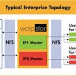
With every process node and every SOC design, engineering and IT teams are experiencing an unprecedented data explosion. User workspaces routinely exceed 10’s of GB and sometimes even 100’s of GB. Regression runs, characterization runs, design and debug of workspaces, building verification environments – all of these put a great stress on Network Attached Storage (NAS) and Cloud resources, create NFS and IO bottlenecks, and cause significant project delays. And things are only going to get worse.
WarpStor is a Content Aware optimizer and accelerator that works to dramatically reduce workspace storage requirements, engineering workspace creation time, network IO bandwidth, and provides almost “lightspeed” data sync whether you are using on premise storage, cloud storage, or both.
Unlike other systems, WarpStor optimizes user workspaces at build time. It does not require any kernel level changes on the client machines, and it does not require post-processing like some data-deduplication technologies. It works in real time and scales easily as needed. For example, additional WarpStor instances can be added at any time on premise, across the enterprise at remote datacenters, and to the cloud, all without disrupting ongoing projects. WarpStor provides its benefits through the use of proprietary technology that creates and manages workspace ‘Masters’ and ‘Clones’. It is transparent to all users. Workspaces are built as fully functional ‘Clones’ of an existing master. These clones start off nearly empty, but to the OS and applications, they appear like any other set of files on disk. As users or applications modify files in the workspace, WarpStor makes the actual file blocks instantly available in the workspace using highly efficient ‘Copy-On-Write’ technology.
This only makes those blocks within files that have been modified local to the workspace at the time of writing. This ensures that workspaces occupy the minimum possible space on disk, as all blocks that are common between a master and its clones are abstracted away. The results experienced by users are dramatic – incremental data syncs are virtually “lightspeed” across the enterprise, workspace creation time is reduced to seconds from minutes or hours and, at the same time, users can see up to 90% reduction in storage requirements and a corresponding reduction in network IO traffic.
In summary, WarpStor can be viewed as a seamless way to radically reduce your expensive storage requirements and engineering workspace creation and submit times for all design and test related workspaces. It works with your current storage and cloud solutions, your current IT infrastructure, and your current IT policies.
About Methodics
Methodics solutions enable high-performance hierarchical analog/mixed signal, digital, software, embedded software, and SOC design collaboration across multi-site and multi-geographic design teams, assuring full traceability of the use and reuse of important design assets for Functional Safety compliance with such standards as ISO26262 and DO-254. With Methodics, traceability is built into the design process – it’s not added on as an after thought.
Advanced IP distribution, cataloging, and workspace management ensure that no matter where designers are located they have full visibility into the IP available to them and can easily access the corresponding data.
And integration of IP Lifecycle Management with industry-standard data management solutions, such as Perforce, Subversion, Git and others makes designs more efficient and predictable, and with higher quality. This approach ensures data is safe, always available, and that the tools can take advantage of the latest advancements from the software configuration management community.
Our highly scalable and industry proven solutions are ideal for large multinational, multisite SoC design teams as well as for small, specialized design teams. www.methodics.com
By the late 80s it had become clear to me that the Japanese were right. Memories, Microprocessors, and Gate Arrays (As well as ASICs) were what customers wanted then. “Building blocks of ever-increasing complexity” was obsolete. What next? Should I try to become an overnight networking expert? Maybe a DSP expert? Pretty tough to do!! Or — how about programmable logic? That could work!!
MMI (Monolithic Memories Incorporated) and others had introduced field programmable logic products a couple of decades earlier using nichrome fuses – devices that conducted current unless you forced a high current through them and “blew them out”. The high current destroyed the fuses so that they would no longer conduct current. This “off” state would be the new permanent state of the fuse. This was exactly the same concept as the fuses that were in the fuse box of every home back when I was young. (Remember – I’m a dinosaur.) MMI’s programmable logic was great. People loved it. But — the programmable circuits available then (Called PALs) were small — on the order of a few hundred gates when the real demand was for circuits with capacities of many thousands of gates. It was clear to me that a truly field programmable gate array would be a big winner.
I was approached by the board of directors of Actel. They were looking for a new CEO. Their product was to be a field programmable gate array. (Andy Haines came up with the term “FPGA” at Actel in 1989 so they weren’t using the term “FPGA” when they were trying to hire me, but that’s what it was.)
The existing FPGA technology (Xilinx) used large numbers of flip flops to store the configuration data. Xilinx referred to these products as “SRAM Logic Cell Arrays” (Later they changed that to SRAM FPGAs). Actel planned to use antifuses instead of flip-flops. An antifuse is the opposite of a fuse. Antifuses do not conduct electricity unless a very high voltage is placed across them. When that happens the fuses are “burned in”. In other words, they will now conduct current. This “on” state is the new, permanent state of the antifuse.
It seemed to me that SRAM FPGAs had a glaring defect. There are many ways that the state of a flip flop can accidentally be changed. A power supply spike. A power supply brown out. A hit by a proton or ion or by some stray radiation. These are all unpredictable ways that configuration can be lost. To make the problem worse, there was never a good way to know in real time that corruption had occurred. (I think that this is true even today). So — if corruption occurred, the circuit might go merrily on its way producing incorrect results and the user wouldn’t know. It was a recipe for disaster!! Or so I thought. The SRAM technique did have a significant advantage — it allowed you to use a standard foundry process. The antifuse required a handful of tricky extra process steps the foundries didn’t like. But — overall I felt that the antifuse would prevail. The process would eventually become a standard and the reliability benefits accruing to the antifuse would win the day!! Again — so I thought.
Actel’s board of directors looked like an all-star team. Ed Zschau (formerly in the US House of Representatives) was on it. Bill Davidow (One of the most famous marketing guys in the IC industry) was on it. And Carver Mead was on it as well. Carver was a Cal Tech professor with an IQ of about 200 who had co-written a textbook that was used in virtually every university. (The textbook was known as “Mead-Conway”). After some foreplay, Ed Zschau invited me to have breakfast at his home in Los Altos. During the meal, he offered me a job as the CEO of Actel. Wow!!! I had an opportunity to become the CEO of the only antifuse based FPGA company. I love FPGAs! Antifuses will dominate the industry!!!! I’LL TAKE IT!!! WHEN DO I START?
Boy. Was I ever wrong!!! Sometimes I feel like I’ve spent the better part of my life being wrong, but that was the pinnacle. The antifuse did not turn out to be a wonderful thing! Why? First, customers wanted reprogrammability — the ability to change the configuration as many times as might be needed without having to remove the part from the board and pay for a new part.. Antifuses were OTP (One time programmable). If you wanted to change something in an antifuse FPGA, you were out of luck. You had to unsolder it from the board, throw it out, buy a new one, program it, and solder it back onto the board. Customers hated that!!! Second, antifuses required a difficult custom fab process that prohibited us from ever being on an advanced process node (Xilinx was always on the most advanced process nodes.). Those two problems prevented us from competing well in the two biggest and fastest growing market segments – telecom and networking.
I started at Actel in 1988. By the mid 90s my love affair with antifuses had all but ended. It had become clear to me that the SRAM configuration technique was clearly better for the majority of applications in those days. Xilinx and Altera were already there with SRAM products. We had only antifuse products. There’s an old business school case study that goes something like this: Company A dominates a market. Company B comes along later with a better way to do it. Who wins? It’s not obvious. It should shape up into a good fight. That’s the battle I thought we’d be fighting when I joined Actel. It wasn’t. The battle we actually fought was: Company A dominates a market. Company B comes along later with a worse way to do it. Who wins? Duh. ….. By the mid 90s I could see that we would eventually die fighting that battle unless we changed the rules of the game.
Clearly we had to replace our antifuse technology with something better. With what? Good question!! I wasn’t sure. What was clear, though, was that it was going to take time and money! It wouldn’t be fast. It wouldn’t be cheap. And it wouldn’t be easy!! Meanwhile, the job was to figure out some market segments where we could at least compete well in the interim. My favorite marketing book is the 22 Immutable Laws of Marketing. It’s only 140 pages, but they’re 140 pages of real wisdom. Chapter 2 tells you in essence, “Don’t try to horn in on a market that someone else already owns. Figure out a subset of the market that you canown and go after it!!!” And we did. Our successful subsets generally centered around the reliability issues that I spelled out earlier. The big markets like communications and networking weren’t buying into the antifuse concept. But — markets that were super-worried about reliability often saw the Actel advantages. The best of these markets for us turned out to be the satellite market. In general, though, we did pretty well in the military and aviation markets as well as with certain industrial and medical products. Those markets were good to us. They allowed us to be consistently profitable. But —- they were all slow growing markets. Wall Street wants fast growing markets and fast growing sales. I always wanted to be growing faster, but it wasn’t to be. Life wasn’t easy in the antifuse business.
Nine years ago, Microsemi bought Actel. A year ago, Microchip bought Microsemi. Today, the old Actel is a division of Microchip – a highly successful company based in Phoenix.
So —- what became of the antifuse? Actel still ships some antifuse products — mostly into designs that were won long ago — but it’s no longer an antifuse technology-based FPGA company. Under the leadership of Esmat Hamdy, Esam El Ashmawi and Bruce Weyer, (Esmat is a founder who directs technology development. Esam and Bruce took turns running the company after I left), Actel completed our long strived-for transition into being a flash based FPGA company. (To be exact, flash and other newer reprogrammable NVM technologies). Flash FPGAs retain the benefits of antifuses, but are reprogrammable and use a process that’s much closer to standard. Sales are rising and profits are very, very solid. Actel is on a roll!! Steve Sanghi made a wise acquisition!* Actel and Microchip are thriving together thanks to the folks who have been there making things happen for so long – many of them for 20 years or more.
(Good to see you the other day!) We owe you a lot!!!
Next week: Foundry woes
*No surprise there. Steve (CEO of Microchip) does things right.
Pictured : From left to right
Bill Davidow. Former General partner of Mohr-Davidow Ventures. Author of three books on High Tech including the immensely popular “Marketing High Technology”.
Carver Mead. Former professor at CalTech. Co-author of “Introduction to VLSI Design.”. Involved in the founding of more than 20 high-tech start-ups.
Ed Zschau. Former member of the US House of Representatives. Former professor at Stanford. Founder of Systems Industries. Former General Partner of Brentwood Associates. Former CEO of Censtor.
In this second article about China’s role in the global semiconductor industry I analyse the impact of the Chinese government’s Big Fund and compare Chinese investments in semiconductor R&D with those in other countries. In my previous article, I looked at the possible effects of a US-China decoupling in the semiconductor industry. Both articles are available in Chinese as well: decoupling, Big Fund (文章翻译成中文:脱钩,大基金).
The Chinese government has made no secret of its ambitions to further develop the domestic semiconductor industry. In May the Chinese Semiconductor Industry Association (CSIA) reported that the value of China’s integrated circuit (IC) imports reached $312 bn in 2018 and has been higher than the value of crude oil imports for some years already. The “Made in China 2025” policy, published in May 2015, mentions specific targets to increase self-sufficiency in IC production to 40% in 2020 and 70% by 2025. It is clear that China aims to accelerate the development of the semiconductor industry and reduce the reliance on imports of chips.
To help reach these goals, the Chinese government established the China Integrated Circuit Industry Investment Fund (CICIIF) or ‘Big Fund‘ in September 2014. The Big Fund was set up to invest in and promote mergers and acquisitions in the semiconductor industry. Beijing envisioned spending more than $150 billion over 10 years to stimulate developments in semiconductor design and manufacturing.
The Big Fund is a government-guided investment fund and operates as a corporate entity under the Ministry of Industry and Information Technology and the Ministry of Finance. The largest shareholders include the Ministry of Finance (36%) and several state-owned enterprises (SOEs), such as China Development Bank Capital (22%), China Tobacco (11%), E-Town Capital (10%), and China Mobile (5%).
The national government encourages local governments, SOEs, private capital, and even overseas investors, to participate in the Big Fund. But since the government is one of the investors it should be considered a government-guided fund according to the National Development and Reform Commission (NDRC). The NDRC lists seven areas for government funds to invest in, which include ‘strategic emerging industries and advanced manufacturing industries,’ and ‘innovation and entrepreneurship.’
Round One: The Big Fund raised CN¥138 bn ($22 bn) in its first tranche in 2014.
One of the major players in the Chinese semiconductor industry is mainland China’s largest foundry Semiconductor Manufacturing International Co. (SMIC). In February 2015, the Big Fund became HK-listed SMIC’s second biggest shareholder acquiring 4.7 billion new shares for HK$ 3.1 bn ($400 M). Currently, the fund holds almost 16% of SMIC’s shares (right behind Datang holding 17%).
Another major transaction involving the Big Fund in 2015 was the $780 M buyout of Singapore-based STATS ChipPAC, the world’s fourth largest chip-packaging and testing company at the time, by Jiangsu Changjiang Electronics Technology (JCET). The buyout included a $240 M investment by the Big Fund and a $150 M investment by a subsidiary of SMIC (SilTech). It instantly made JCET the number three packaging and testing firm in the world.
The Big Fund has been used to support the creation of a joint venture between Nantong Fujitsu Microelectronics (now known as Nantong Tongfu Microelectronics, TFME) and AMD Penang (Malaysia) and AMD Suzhou (China) in April 2016. With AMD‘s world class assembly and test technologies TFME aims to develop into a global Outsourced Semiconductor Assembly and Test (OSAT) company.
In March 2017 Tsinghua Unigroup signed a deal to receive up to CN¥150 bn investment, two-thirds coming from China Development Bank and one third (no less than $7 bn) from the Big Fund. The company did not provide any specific details how the money would be used, other than upgrading its R&D and scale up its operations. Tsinghua Unigroup acquired Spreadtrum Communications and RDA Microelectronics in 2013 and 2014 respectively. Its subsidiary focused on R&D of core chipsets for mobile communications and IoT is now known as UNISOC and is China’s second largest mobile chipmaker, after Huawei’s HiSilicon.
Last year January SMIC set up a joint venture with the Big Fund and the local government’s Shanghai IC Fund focusing on 14nm and below process and manufacturing technologies. The Big Fund invested $947 M for 27.0% of shares, Shanghai IC Fund invested $800 M for 22.9% of shares and SMIC invested $1.54 bn to be Semiconductor Manufacturing South China’s (SMSC) majority shareholder holding 50.1% of shares.
In the first round, the Big Fund invested in more than 70 projects and companies, some of whom are listed on the Hong Kong, Shanghai, Shenzhen and NASDAQ stock exchanges. These include above-mentioned Tongfu Microelectronics (Big Fund holds 22% of shares), JCET (19%), and SMIC (16%). But also test equipment company Changchuan Technology (7%), wafer cleaning technology company ACM (6%), etch tools and MOCVD system maker Advanced Micro-fabrication Equipment Inc. China (AMEC, listed on the Shanghai Stock Exchange STAR Market since July 22), equipment maker NAURA Technology Group, and Yangtze Memory Technologies Co. In all these cases, the Big Fund did not become the majority shareholder through its investments, which is in accordance with a statement of fund President Ding Wenwu in 2015 that the Big Fund did not seek to become the largest shareholder of the companies it invested in.
This is not necessarily the case for other funds the Big Fund participates in. In May 2018, the Big Fund joined a group of companies to set up the $244 M IPV Capital Global Technology Fund to invest in semiconductor companies. The Big Fund committed $121 M and controls 49.5% of the fund, L&L Capital 39.29%, SMIC’s subsidiary China IC Capital 10.21%, and IPV Global 1%.
Round Two: The Big Fund raised CN¥200 bn ($29 bn) by July 2019 in its second tranche, which was announced in March 2018.
Last month the fund raising for the second tranche of the Big Fund was completed with a total commitment of CN¥200 bn ($29 bn). New investments will likely be more focused on applications in the downstream supply chain of the semiconductor industry, such as chip design, advanced materials, and tools and equipment. Considering the investment priorities for 2019 as mentioned by the NDRC: Artificial Intelligence (AI), the industrial internet, Internet of Things (IoT), and 5G, promising chip design companies in these areas could be looking at an interesting year ahead if they are looking for funding.
Big Fund = Big Impact?
In its first two rounds, the Big Fund has raised an impressive total of $51 bn. But exactly how impressive is this in the capital- and R&D-intensive semiconductor industry?
The American Semiconductor Industry Association (SIA) writes in its April 2019 report‘Winning the Future – A Blueprint for Sustained US Leadership in Semiconductor Technology’ that “Technology challenges and ambitious steps by foreign governments put at risk continued semiconductor innovation and US leadership in this sector. (…) Although US companies still lead the world with nearly half of global market share, state-backed competition from abroad seeks to displace US leadership.” And more specific on the potential impact of the Big Fund: “The Chinese government has announced efforts to invest well over $100 billion over the next decade to catch up to the United States in semiconductor technology, artificial intelligence, and quantum computing. While China may not meet all its goals, the size and scale of its effort should not be ignored.”
In the remainder of this article, I analyse the size and scale of R&D spending and investments in the semiconductor industry for the most relevant countries in the industry. For each of them I looked at the R&D spending of their most important semiconductor companies and, if available, data on semiconductor R&D specific government funds or investments. I have to note it is very challenging to find (reliable) data on government funding or investments specific to the semiconductor industry. As the focus is on semiconductor industry R&D, I have not looked at government funding for purely academic research. Therefore, the data is definitely not complete, but I believe it still gives a general idea about the differences in semiconductor-related R&D and investments in these countries.
For industry R&D expenses, I looked at a selection of semiconductor companies active in the entire value chain, including chip design companies, equipment makers, and chip production companies. The last category includes front-end wafer fabrication as well as back-end testing, assembly and packaging. This R&D data is more readily available from the companies’ annual reports. I only included companies that have annual R&D expenses exceeding US$100 M, except for China. Because the Chinese semiconductor industry is not as mature yet, the focus of this article is on the potential impact of the Big Fund, and including more Chinese companies probably means learning about new companies for many readers, I decided not to use this threshold for Chinese industry R&D expenses.
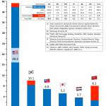
US American semiconductor companies have by far the highest R&D expenses. Intel’s R&D spending of $13.5 bn in 2018 (19% of sales) is far higher than any other company in the world. Within the US, Intel is followed by Qualcomm ($5.6 bn, 25%), Broadcom ($3.8 bn, 18%), Nvidia ($2.4 bn, 20%), Micron ($2.1 bn, 7%), Applied Materials ($2.0 bn, 12%), Texas Instruments ($1.6 bn, 10%), AMD ($1.4 bn, 22%), Lam Research ($1.2 bn, 11%), Marvell ($914 M, 32%), Xilinx ($743 M, 24%), ON Semiconductor ($651 M, 11%), KLA ($609 M, 15%), Maxim Integrated ($451 M, 18%), Cypress Semiconductors ($364 M, 15%), Teradyne ($301 M, 14%), and Amkor ($157 M, 4%). Together, these 17 companies spent $35.8 bn (16% of their combined sales of $234 bn) on semiconductor research and development. Per year! In the ‘Winning the Future’ report, SIA urges the US government to triple US investments in semiconductor-specific research from the current $1.5 bn to $5 bn annually, to ensure continued US leadership in the global semiconductor industry.
South Korea On April 30, South Korean President Moon Jae-in spoke at the ceremony to unveil Korea’s ‘System Semiconductor Vision’: “We will expand government R&D in the semiconductor field, giving top priority to promising technologies in high demand. Starting next year, a technology development project worth one trillion won ($0.86 bn) will be pursued as part of the efforts to secure original technologies for next-generation semiconductors.” As a reaction to Japan’s tightening of semiconductor materials exports to Korea, the Korean government also recently announced plans to invest 1 trillion won annually ($0.86 bn) to develop semiconductor materials. Samsung’s reported semiconductor revenue is $77.2 bn, but the annual report does not mention R&D spending for its semiconductor division. R&D expenses as percentage of sales for the whole company are 7.5% and considering semiconductor sales represent 35% of Samsung’s total sales, I take $5.8 bn (7.5% of $77.2 bn) as an estimate for Samsung’s semiconductor-related R&D expenses. With SK Hynix reporting R&D expenses of $2.6 bn in 2018 (7.1% of sales), Korea’s two semiconductor giants spent $8.4 bn (7.4% of their combined sales) on R&D.
Taiwan TSMC is the semiconductor industry’s top R&D spender in Taiwan with $2.9 bn, or 8.3% of sales. MediaTek follows with $1.9 bn (24%), before ASE Technology Holding ($490 M, 4.0%), UMC ($427 M, 8.6%), Realtek ($425 M, 28%), Novatek ($254 M, 14%), Winbond ($252 M, 15%), and Nanya (NTC, $160 M, 6%). These 8 Taiwanese semiconductor companies spent $6.8 bn or 10% of their combined sales ($66.1 bn) on R&D. President Tsai Ing-wen mentioned last year that the government is committed to developing Taiwan’s semiconductor sector and providing all requisite assistance for local firms upgrading competitiveness and retaining leadership positions. However, I did not find any specific details on governmental research funding or investment support for the semiconductor industry.
Japan Renesas leads semiconductor R&D spending in Japan with $1.1 bn (17%), followed very closely by Sony Semiconductor Solutions ($1.1 bn, 14%). Toshiba Memory has separated from Toshiba and will continue as Kioxia Holdings, but Toshiba Memory’s R&D expenses in the year ending March 2018 were also $1.1 bn (10%). Tokyo Electron’s R&D expenses were $1.0 bn or 9% of sales in 2018. Rohm Semiconductor follows with $357 M (10%), Advantest spent $341 M (13%) and Dainippon Screen spent $206 M on R&D (6%). Together these seven companies spent $5.2 bn on R&D (10% of their combined sales of $49.6 bn). I did not find any information on government funds for R&D or investments in the Japanese semiconductor industry.
The Netherlands In the Netherlands the only recent semiconductor-related government investment is a $86 M investment for a public-private photonics initiative. The top 3 Dutch semiconductor companies spent a combined $3.6 bn on R&D (16% of their combined sales of $22.7 bn). ASML leads Dutch semiconductor industry R&D investments with $1.8 bn (14%), followed by NXP ($1.7 bn, 18%), and ASM International ($101 M, 11%).
China HiSilicon is most likely China’s biggest semiconductor R&D spender but it does not publish financial data. HiSilicon’s 2018 revenue is reported to be $7.3 bn. Taking parent company Huawei’s R&D expenses as percentage of sales (14%) as a proxy, HiSilicon’s R&D expenses would be around $1.0 bn. For UNISOC I take a similar approach. Using parent company Tsinghua Unigroup’s R&D expenses as percentage of sales (30%) for UNISOC’s revenue, their estimated R&D expenses are $480 M. For one more non-listed company, Beijing OmniVision, revenue is reported to be more than $1.0 bn but I did not find any information on their R&D expenses. For China’s listed semiconductor companies, SMIC spends by far the most on R&D reporting $558 M R&D expenses in 2018 (15% of sales). Packaging and testing company JCET spent $129 M (4%), followed by IC design company Goodix, who recently acquired NXP’s Voice and Audio Solutions, with $121 M (23%). TFME spent $81 M (8%), Tianshui Huatian Technology $56 M (5%), equipment maker NAURA $51 M (11%), pure-play foundry HHGrace $45 M (5%), GigaDevice $30 M (9%) and equipment maker AMEC $17 M (7%). Combined, these eleven Chinese companies’ R&D expenses are $2.6 bn, or 13% of their combined sales ($20.3 bn).
The industry R&D expenses for all companies except Samsung, HiSilicon and UNISOC are derived from the companies’ annual reports. To compare annual R&D expenses and investment, I divide the money raised by China’s Big Fund in its first round ($22 bn) over 4 years (2015-2018), which results in an average annual budget of $5.5 bn.
Industry and government spending on semiconductor R&D
Figure 1: Industry and government spending on semiconductor R&D
Figure 1 shows that only in China the government’s semiconductor investments are (much) higher than the companies’ R&D expenses. For example, the government’s investments in China are more than 2 times as much as industry R&D expenses. Whereas in the US, industry’s R&D expenses are 25 times as much as the government’s semiconductor-specific research funding.
However, it is not completely clear how much of the Big Fund’s first round funding has been spent until now. The assumption that $22 bn has been spent over 4 years (2015-2018) may not be completely accurate, but it’s my best guess. When the Big Fund was established in 2014, the plan was to invest more than $150 bn in ten years, which amounts to an average annual spending of $15 bn. This is considerably more, but still not much more than Intel’s current annual R&D expenses of $13.5 bn. Including the second round, the Big Fund has raised $51 bn until now, but we are also halfway the original 10 years horizon. So, either the initial goal of raising $150 bn was overly enthusiastic or the government has to accelerate fund raising.
Comparing semiconductor R&D spending across countries, it is clear from Figure 1 that the R&D expenses of Chinese companies lag behind those of other countries, even including the six Chinese companies that spend less than $100 M on R&D. It should also be mentioned that many Big Fund investments are not targeting R&D per se. Actually, a lot of funding so far has been used for expanding fab capacity (e.g., SMIC, SMSC, HHGrace, Huali, Yangtze Memory Technologies). Building more capacity for current technology nodes may help to increase sales and thus potential future R&D expenses, but the global semiconductor industry keeps moving ahead. If China does not invest more in R&D, it will continue to be very challenging to catch up from a technology perspective.
Conclusion
Does the Big Fund have a Big Impact on the development of the Chinese semiconductor industry? Yes. More investments in China’s semiconductor industry are required for China to achieve its goals of increasing self-sufficiency in IC production and accelerating the development of the domestic semiconductor industry. And $150 bn is a lot of money.
But… The impact of the Big Fund should also be put in perspective. The size and scale of China’s effort to invest in semiconductor technology is impressive, for a government fund. However, the R&D expenses of semiconductor companies in some other countries are at least as impressive. There are many companies in the semiconductor industry that spend more than $1 bn on R&D every year. I mentioned 20 in this article, but there are more (e.g., ST Microelectronics), and some are very close to the $1 bn mark (e.g., Marvell and Infineon). Figure 1 shows that the US is still far ahead of all other countries when it comes to semiconductor R&D. Actually, the top 10 US semiconductor companies, ranked by R&D spending, together spend more on R&D every year than all industry and government spending of the other countries combined ($34.5 bn vs $33.9 bn). So, the Big Fund does definitely not instantly make China the global leader in semiconductor R&D investments. Moreover, the Big Fund’s investments are not all focused on technology development, but for example at increasing capacity and acquiring existing technology. There is still a long way to go before China is winning the future and leading innovation in the semiconductor industry.
My first IC design back in 1978 was a DRAM and it ran on 12V, 5V and -5V, but then my second DRAM was using only a 5V supply. Today we see SOCs running under a 1V supply voltage, but there is a totally different market for power devices that are at the other end of the voltage spectrum and they handle switching ranges from 12V – 250V. To learn more about power devices and how the process and device modeling is done, I read a Silvaco publication entitled Advanced Process and Device 3D TCAD Simulation of Split-Gate Trench UMOSFET.
For vertical discrete power MOSFETs there are two important specifications that engineers look at:
Breakdown voltage (BV)
Specific on-state resistance (RSP)
A couple of approaches have been used for power devices: Trench MOSFETs, RSO MOSFETs. The winning approach has been the Split-Gate RSO MOSFETs because of their low channel resistance, plus ultra-low drift region resistance with a smaller Cgd (gate-to-drain capacitance), improving switching speeds.
Process engineers use 3D TCAD tools to model power devices and optimize them by looking at the predicted values of:
Capacitance-Voltage (C-V)
Current-Voltage (I-V)
Breakdown Voltage (BV)
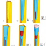
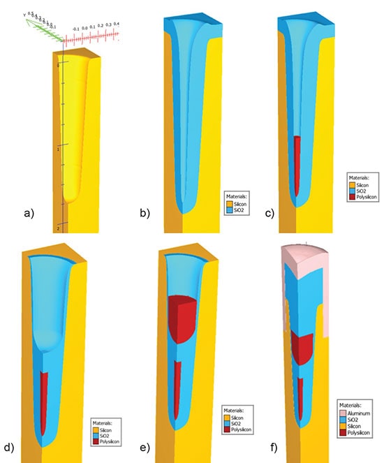
Silvaco provides Victory Process and Victory Device simulators to do this modeling of power devices. So let’s start with a 3D process simulation of a Split-Gate UMOSFET, where Victory Process is used to build the device structure. Several simulated process steps are shown below:
a) Formation of a deep trench with rounded bottom, both dry and wet etch steps
b) Shield oxide growth
c) Shield poly deposition
d) Inter-poly oxide deposition and etch back
e) Gate poly deposition and etch back
f) Core contact etching and deposition of the contact plug
Victory Process simulation of key process steps to fabricate the Split-Gate UMOSFET
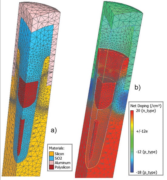
A 3D numerical mesh is the next step using the Victory Mesh tool, and a 3D Delaunay mesh was generated to accurately resolve the 3D geometrical features. Here’s the result of meshing:
Delaunay mesh to resolve complex 3D geometry features (a) and doping profiles (b)
3D device simulations are then run with the Victory Device simulator, and this is quite powerful because it can model 3D unstructured tetrahedral meshes for any device shape. To run Victor Device simulations you have several actions:
Specify the materials, models and simulation values
Simulate steady-state Id-Vg, gm-Vg, Id-Vd and BV
Small-signal (AC) capacitance-voltage (C-V) plot
Device switching plots
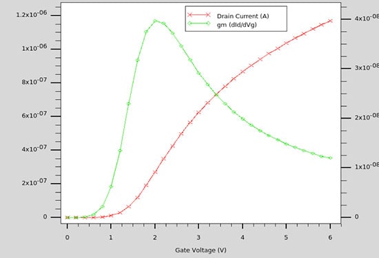
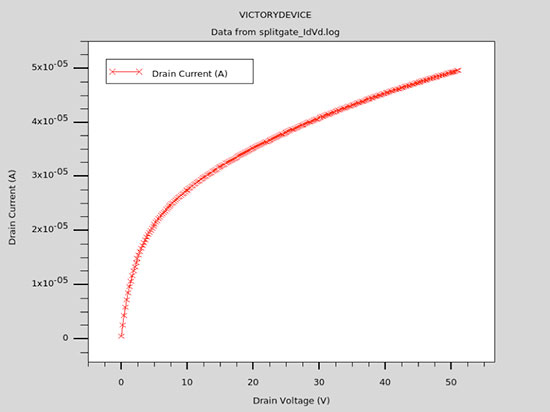
An initial solution is computed, then Id-Vg curves are produced for each Vds voltage, then transconductance gm-Vg are computed as shown below:
Computed Id-Vg curve (at Vd=0.1V) and extracted transconductance gm-Vg characteristics
Here’s the plot of Id-Vd at a select Vgs bias voltage:
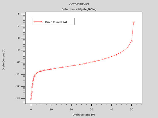
A plot of Breakdown I-V is shown where the gate bias Vg = 0V:
Computed Breakdown I-V characteristics, for Vg=0V
Each of these I-V curves was generated by the TonyPlot tool.
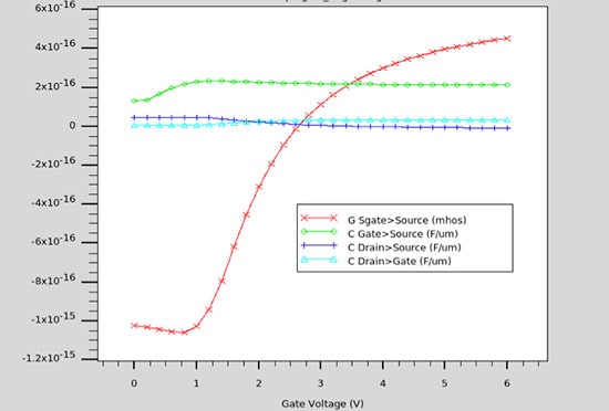
C-V plots are simulated with Victory Device, and here’s the small-signal (AC) results showing intrinsic capacitances:
Computed device Capacitances versus Gate Voltage (Vg)
Summary
Process engineers equipped with the proper modeling and simulation tools can now predict the behavior of power devices like Split-Gate Resurf Stepped Oxide (SG-RSO) MOSFET. Instead of running lots of silicon, measuring, tweaking and repeating, engineers can accurately model and optimize virtually, saving lots of time and money. Read the complete article online.
Gross Profit Margin Percent Provides a Measure of Product Value
The difference between what customers will pay for a physical product and what it costs to make or acquire it is a good measure of differentiation. This difference divided by the revenue is the gross profit margin percent or GPM%. Once a product has an established market share, difficulty of switching to another product usually maintains or enhances the GPM% even if the product differentiation diminishes.
At the time the Apple iPhone was introduced in 2007, it was priced at $749 “unlocked” (i.e. without service provider subsidy) compared to commodity cell phones that sold for $15 at the same time (Figure 1). Why would anyone pay fifty times more for a product that did the same thing – made phone calls and sent text messages? Apple proved that there was much more differentiation possible.
Apple’s previous attempts with differentiation encountered some difficulties (Figure 2). Before the IBM personal computer was introduced, Apple was able to capture one third of the PC market and maintain a GPM% between 40% and 50%. After the Macintosh introduction, Apple returned to 50% GPM for a while but its market share had dropped to about 20%. Apple then introduced the Mac Classic priced to compete with IBM. This and the introduction of Windows 95 by Microsoft drove Apple’s GPM% down to 10% along with its market share. As Apple’s market share subsequently declined to 5% shortly after 2001, GPM% became negative. The iPod and iPhone reversed this corporate trend, bringing the MacBook along with them and resulting in a corporate GPM% of 40% in 2010 and a $999 price for a MacBook that was roughly twice the price of equivalent IBM-compatible PCs. Even today, Apple PCs sell for nearly double the price of the IBM-compatible PC of “equivalent” capability.
Apple’s differentiation after 2001 came from more than just the products themselves. Apple built an interdependent ecosystem that made it difficult to switch suppliers if you committed to any part. The infrastructure included iTunes, Apple stores, Genius Bars and MobileMe/Cloud. But the best part of any ecosystem is the part that isn’t paid for by the supplier. In Apple’s case, that meant the connectors in cars and hotels, the third-party apps on the iPhone and Mac, the peripheral devices, and many more (Figure 3).
Figure 1. iPhone differentiated value versus commodity cell phones
End product companies are not the only ones who have achieved differentiation that translates into GPM%. Even component suppliers can do this (Figure 4). Intel’s 8088 16-bit microprocessor was arguably the worst of its generation. Clearly superior products were introduced (within a year) by Motorola and Zilog. Combining “first to market advantage” with some legal protections through extension of copyright law to semiconductor photomasks, Intel was able to create a highly differentiated dynasty of products with high switching costs that today dominate the computer server business.
Figure 2. Apple GPM% and market share
Figure 3. Building an ecosystem to make switching more difficult for existing users
Figure 4. Intel component differentiation
Can a Commodity Product Be “De-commoditized”?
Before all the suppliers of “commodity” products become depressed, let’s consider the question of “de-commoditization”. Don’t give up hope. There are lots of examples. Consider Figure 5. Water is generally available for $0.0002 per glass. Yet, in the last few decades, innovative companies have found ways to sell water for $0.75 per glass. A similar, but less extreme, scenario could be described for coffee.
I was personally involved in one of the more notable cases of de-commoditization in electronics. In 1977, I was Engineering Manager for Texas Instruments’ (TI) Consumer Products Group. TI had aggressively reduced the component count of a basic four-function (add, subtract, multiply, divide) calculator from 480 components in 1971 to a single chip in 1977 (Figure 6).
Pretty impressive, don’t you think? TI must have made a lot of money from those innovations? Actually, no, they didn’t. The four-function calculators continuously lost money although the scientific calculators made up for much of the loss.
Figure 5. De-commoditization of water
The losses became so painful that TI finally resorted to OEMing (selling calculators manufactured by other companies) as shown in Figure 7.
De-commoditization wasn’t easy. But TI had an example to follow from early history with a product called the “Little Professor” which was designed to teach arithmetic. It had a life of its own. Unlike other calculators, the sales continued despite recessions and obsolescence. We learned that parents will pay whatever is required to give their children an advantage in school.
Figure 6. Innovation reduced component count of electronic calculators from 480 to one component in five years
Armed with this history, the TI Consumer Products Group focused on the education market. Over the next two decades, they worked with teachers, school boards, educators, course developers and the entire educational ecosystem to develop a program geared to their graphing calculators. Figure 8 shows TI calculators that are both differentiated and commoditized. The TI-89, shown on the left, sells for $150. I have personally bought six of these. My two daughters lose them, loan them to friends, break them or require different versions for different classes. TI probably OEMs them for less than $20 each.
Figure 7. TI begins “OEMing” calculators made by foreign manufacturers
For TI, a money losing calculator business has now become one of its most profitable businesses. Figure 9 shows the reported segment profit for TI calculators. In 2007, GPM % for TI calculators had reached 65%, at which point TI stopped reporting this segment. As a former TI executive, I have concluded that the reason TI stopped breaking out the reporting of this segment is that it became embarrassingly profitable – more so than the semiconductor component businesses of TI.
Figure 8. Differentiated and commoditized TI calculators
Figure 9. TI’s education focus leads to an Increasingly profitable calculator business
What about semiconductors? Historically, the industry grew with very limited differentiation. Faster, better germanium transistors were quickly matched by competitors because the original AT&T licensing program created a level playing field for semiconductor patents. TI gained a two-year advantage with the silicon transistor but that was soon matched as well. Integrated circuit designs were easily copied and customers had sufficient power to force semiconductor suppliers to have an alternate source of supply for their designs before the customer would “design in” the product.
Over time, semiconductor companies found ways to create differentiation. The most common type is the differentiation that comes with analog components because they can be differentiated by both the design and the manufacturing process. As a result, pure analog companies like Analog Devices and Maxim have demonstrated consistently high GPM%. Most knowledgeable people are surprised to learn that analog components are not the highest consistent GPM% products — Field programmable gate arrays, or FPGAs are. Like analog components, FPGAs carry high switching costs once they are designed into a product (Figure 10). FPGAs have an additional barrier to switching suppliers that extends across the entire component product line — differences in the way different manufacturers’ FPGAs are programmed creates a barrier for designers to switch suppliers. In addition, libraries of proven reusable blocks of a design are built up in a company over time and are difficult to re-create.
Figure 10. FPGAs have consistently provided the highest GPM% in the semiconductor industry
Next highest GPM% among major semiconductor categories, after FPGAs and analog, is the microprocessor. These can be differentiated by their computer architectures and embedded software microcode that can be copyrighted. Patents in the semiconductor industry are difficult to enforce because most large companies are cross-licensed and, even when a patent lawsuit is successful, the precedents for royalties are small, usually less than 5%, assuming the licensee doesn’t have any patents that can be used as bargaining chips against the licensor.
Intel’s de facto standard 808X microprocessors would probably be commodities today if Intel hadn’t followed a unique path, i.e. enlisting the forces of the U.S. government to extend copyright legislation to the photomasks for semiconductor components in 1984. The act of copying physical objects that are copyrighted had always been protected before 1982. If you saw a building you liked, you could build one just like it and incur no liability unless you stole the plans from the architect or owner. Intel’s “Semiconductor Chip Protection Act” of 1984 prohibited direct physical copying of chips, even though it had been standard practice in the industry until that time. This limited competing 808X microprocessor suppliers to the Intel-licensed source, Advanced Micro Devices (AMD), and companies that utilized Intel cross-licensed companies like TI for manufacturing. Cyrix was one example of a company that circumvented Intel’s barriers by using a licensed manufacturer, TI . In addition, Intel was careful to keep their pricing near the learning curve so that competitors like AMD could be held to a small market share.
Figure 11. 2009 – 2010 GPM% for major semiconductor component categories
Figure 11 shows the GPM% of major semiconductor product categories. There is GPM% differentiation within each category due to other factors such as existing market share. Categories with high switching costs, like FPGAs and microprocessors, tend to have one or two suppliers at the high end of GPM% and others below.
Commodity products like memory and discrete devices are more difficult to differentiate partly because their commodity nature is core to the value perceived by customers. Most customers wouldn’t design in a DRAM that has no “pin compatible” alternate sources.
What can semiconductor companies do to increase their average GPM%? Figure 12 offers some suggestions.
Figure 12. Other ways that semiconductor component companies can enhance GPM%
Semiconductor companies have a difficult time differentiating on price, quality of support, sales distribution and many approaches that work in other industries. In general, even manufacturing process differentiation is difficult to sustain for more than one technology generation. Design offers more opportunities to differentiate, especially with “system on a chip”, or SoCs, that are sourced by only one supplier. If they incorporate complex algorithms and copyrightable microcode, so much the better. Combinations of process and design, as with analog, RF and power devices, is even better. This benefit accounts for the general movement of companies like TI, NXP and others to an analog-rich portfolio.
Reusable IP blocks are becoming commoditized. There is still an opportunity, however, to develop proprietary IP blocks, as companies like Qualcomm have done, to facilitate superior performance or time to market.
Finally, the best differentiation is that created and paid for by customers. ARM is a successful example of a company that built a niche in low power embedded microprocessors for wireless handsets and then expanded to a variety of other applications. Third parties provide a wide variety of assistance, interfaces to other IP, endorsements, etc.
Another example is the effectiveness of open sourcing of a product that increases the value of a proprietary one. Adobe did this with Acrobat. In semiconductors, one of the most impactful moves was from TSMC. Until the late 1980s, silicon foundries kept their “design rules” secret. Customers signed non-disclosure agreements just to find out the information needed to evaluate the viability of a particular foundry for the capabilities the designer needed. TSMC management was frustrated by the share of their business that came from designs that were developed using someone else’s design rules, forcing TSMC to tweak their process to match the results provided by the other foundry. Compass Design Automation, a subsidiary of VLSI Technology, even provided a design library called “Passport”. It was popular with designers because, if you used the cell libraries in Passport, multiple foundries had a manufacturing flow that would accommodate the design and produce the same results as the simulated ones. TSMC went one step further by removing secrecy restrictions on their design rules. Compass found it easier to adopt the TSMC design rules for their library, thus solving TSMC’s problem. Now all the other foundries had to tweak THEIR processes to match the TSMC results. Effectively, a large share of the foundry customer base became standardized on TSMC’s design rules and process.
For the future, the biggest differentiation challenge of the semiconductor industry comes with the Internet of Things. IoT sensors, actuators and controllers are projected to sell in very high volumes at very low prices. Achieving reasonable GPM% is difficult. In the world of IoT, the profit goes to the owners of the information collected from the network of sensors and data collection sites rather than to the providers of the IoT components. As a result, companies like Google, Amazon, automotive OEMs and others are designing their own chips to deploy in information collecting networks. In these environments, the same company can design and own the IoT sensors and the information collected. Semiconductor companies with IoT component businesses are trying to figure out how to couple their design and manufacture of the components in a joint venture with those who analyze the data. This is a difficult sale so it’s likely that we will see continued entry of systems companies into the world of SoC design.
Information and figures in this Chapter are covered in greater detail in a You Tube video entitled “Value From Differentiation” presented at the ARM TechCon in 2011 (below).
Surrogate Wars
Is GloFo using the trade war as an excuse?
Does TSMC get lumped in with China on trade?
Does this alienate TSMC into China’s embrace?
Much like Vietnam and Korea before it, there have been a number of “surrogate” wars between the US and China as well as many other wars between the US and Russia using other surrogates.
Though it may or may not be the intention of the current administration to make the lawsuit between Global Foundries and TSMC a surrogate trade war, it certainly has the right script. A US based company, Global Foundries, is suing a “China” based (cause thats what China says Taiwan is…) for intellectual IP and patent infringement. GloFo even has at its technology heart, the once proud, now rusting, old IBM technology base, that back in the day was a technology leader now blown past by TSMC (read that as China). It conjures up the standard “China is killing US industry” image as GloFo has wrapped an American flag around itself.
(We will omit the inconvenient truth that GloFo is setting up shop in China mainland along with TSMC).
A “Twitter Ready” Lawsuit
The lawsuit by GloFo against TSMC seems to be a “twitter ready” set up for someone to come along and hit it out of the park. The timing is obviously very suspect given the current trade war issues with China and many politicians looking for more excuses and ammunition.
It paints TSMC (and Taiwan) as the enemy & part of China
The problem we have is that the lawsuit obviously paints TSMC and Taiwan with the same broad paint brush as China.
Since when did TSMC & Taiwan become the enemy of the US and the US industrial base?
Follows in the footsteps of Hong Kong
We had warned in a recent newsletter that we were concerned that Taiwan could become the next Hong Kong as the Chinese could be emboldened by the administrations “abandoning” of Hong Kong by saying “its none of our business because Hong Kong is part of China”.
Could this lawsuit further embolden China towards Taiwan if the US administration distances itself further from Taiwan and views Taiwan as part of the China trade threat against the US heartland? If the administration takes the GloFo side that would seem to be the case.
Could TSMC run into China’s open arms?
If it looked like the US government were taking sides against TSMC they may not have a choice but to seek refuge.
UMC (TSMC’s competitor) is already deep within China’s embrace as they clearly had a hand in stealing some of Micron’s IP from Taiwan to mainland China in the case of Jinhua.
TSMC obviously is building up fabs in China and could decide to move more operations there or bring more technology thus accelerating “made in China 2025.
It depends a lot on how the current US administration plays this and how much they take sides.
GloFo reaching out from the grave
Given that Global Foundries gave up the race to be a technology leader in the semiconductor industry a year ago when it abandoned advanced technology, they now don’t have a lot to lose by starting a war against TSMC related to leading edge process. Theres not a whole lot TSMC can do to shut down GloFo’s advanced technology through legal means as GloFo already shut it down themselves. TSMC on the other hand has a lot to lose as the technology leader with the biggest customers.
GloFo clearly lost the technology & production war with TSMC in the market and this may be a bit of a revenge or sour grapes or both….except that the real reason is money….
Squeezing money out of a dead fab
It has long been rumored that Abu Dhabi is looking to unload GloFo and we have seen parts already sold off. Recently the mask operations were sold off and some ASML EUV scanners have already been sold off as part of the leading edge equipment yard sale.
It would seem very logical that GloFo would seek to monetize any and all assets to maximize a sale value or cash return on their way underwater investment. TSMC could decide the risk is too big (especially if the US government backs GloFo) and just pay a royalty to GloFo. In fact the current administration would probably trumpet a “China based” company paying a royalty to a “wronged” US company. So its not too far out of the question
Stuck in a “Catch 22”
We see the current situation as a bit of a “catch 22”. If the US sides with GloFo, it alienates TSMC and Taiwan whom have been great partners and the key enablers of US technology. If it sides with TSMC, it will be seen as against US based companies and for Chinese IP theft. If it doesn’t take a position it will be seen as ignoring a major trade and IP theft issue with China….the issue that has been the hallmark of the administration.
Its a bad situation and GloFo may have put the administration in a box at a sensitive time.
Summary:
While we certainly have been very vocal about US and China trade and IP issues, the GloFo and TSMC lawsuit has absolutely zero to do with them and is not part of the overall larger trade & IP issue even though GloFo would like to make it so.
The semiconductor industry is a virtual landmine field of patents that make it almost impossible to manufacture a leading edge device without leaning on someone else’s IP or patents. TSMC is quoted as having 37,000 patents and GloFo got 16,000 from IBM.
Companies collect patents like nations collect nuclear weapons in a game of “mutually assured destruction” in which one doesn’t sue the other as they are afraid of the response. GloFo is no longer in the game so they don’t care, they are already dead.
Its a bad precedent to set and the US is going to have to walk a carefully choreographed tightrope to avoid a mess.
The stocks
All this just adds to the general “overhang” on the stocks related to China trade and adds another variable and another news point to move the stocks.
Other companies like Apple, AMD, Nvidia and other customers and suppliers could get sucked into the vortex as well. GloFo doesn’t care as they aren’t customers and GloFo is private anyway.
It will be a long time to resolve but we would be more concerned about either a near term escalation or involvement of other companies that get hit by collateral damage.


