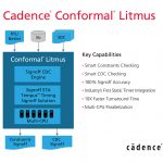
Bronco Webinar 800x100 1

Considering SiFive: What Should I Get to Implement a RISC-V Core?

Considering SiFive: What Should I Get to Implement a RISC-V Core?
by Randy Smith on 06-17-2019 at 10:00 am

I have an old weathered leather-clad black notebook with a National Semiconductor logo on its face that I have used since 2001. It has sentimental value to me. First, it reminds me of where I was on 9/11, having breakfast with a group of attendees to National Semiconductor’s executive event in Laguna Niguel, CA. We were going to play golf that morning and we were watching CNN when the tragic events took place. The notebook also takes me back to that time when I was running sales and marketing for TriMedia Technologies, a Philips Semiconductor spinoff that was producing VLIW core processor IP. ARM was in its early growth phase before increasing its stock ~10x between 2004 and 2015. By 2001, InfoWorld awarded Red Hat its fourth consecutive “Operating System Product of the Year” award for Red Hat Linux 6.1 and open source was well on its way in the operating systems market. It is exciting now to consider what is taking place with RISC-V, an open source core.

It turns out that determining what to include in the delivery of a proprietary soft IP core and an open source core is not that different. You want a dependable company to supply a core that it has tested fully. You need good documentation and a thriving ecosystem. The data file formats are well-known industry standards. But in considering RISC-V, there is another layer here. RISC-V is indeed open source, but it is also quite extensible. Which features do you want to be included and which features do you need? This is where your choice of vendors matters.

I met Naveed Sherwani, the CEO of SiFive many years ago when he was leading Open-Silicon. When we connected by phone last year, I got caught up with what was going on at SiFive at the time. I have not had the chance to talk with him since then, but clearly, SiFive has been very busy since then. Glancing at the SiFive website I see they are now delivering many different standard IP cores, as well as development boards and software. The documentation page lists a dozen core manuals. To have your design be efficient as possible, you need a good choice of cores, but further customization is often needed, and SiFive can provide that as well. I won’t make a comparison with ARM as I was under NDA to ARM while running marketing at Sonics just a few years ago. But clearly, SiFive is off and running now.

The customization tool of SiFive, Core Designer, is quite impressive. Via the SiFive cloud interface you select either 32-bit or 64-bit, then your operating system requirements, and you are narrowed down to a few choices of fully qualified cores. From there you can go on to customize the core you pick with the unique features needed for your application – that is why these are being called “Application-specific processors” (ASP). You can choose from different modes to be supported, the level of pipelining needed, various instruction set architecture (ISA) extensions that are available, the amount and arrangement of on-chip memory, the configuration of various ports (e.g., AHB, JTAG, etc.), security features, debug options, interrupts, and power management options. Quite a bit of customization is available. The speed at which SiFive is building out its IP portfolio is truly amazing.

SiFive is expected to release Chip Designer sometime soon. SiFive claims this will be a new way of building custom silicon. In the design step, you are to choose the template that suits your application. Templates now are shown on the website range from 28nm to 180nm implementations. You can create variations on your design using a library of IP from SiFive’s DesignShare Partners or with your own IP. Prototyping will then allow you to run your application code and make changes to your design until you are happy with the performance. Then you order and SiFive will deliver sample chips in some number of weeks. This is an interesting approach. I have heard of similar approaches elsewhere and I cannot wait to hear the specific details of what SiFive is planning to deliver.

SiFive has indeed come a long way in a very short time. It is amazing to see how the landscape of core processor IP as developed over the past 20 years or so. By delivering cores, tools, prototyping, a large ecosystem and more SiFive seems to have what is needed to move forward quickly with a customized RISC-V core to support your own ASP. Hold on tight – I feel that the next two years will move us at warp speed in comparison.


Intel let there be RAM

Intel let there be RAM
by John East on 06-17-2019 at 5:00 am

The “20 Questions with John East” series continues

Intel was founded in 1968 by Robert Noyce and Gordon Moore who had left Fairchild earlier that year.  They immediately hired Andy Grove. Noyce, Moore and Grove were a study in contrasts. I had various dealings over the years with Noyce and Grove, but have met Moore only twice.  They had some things in common, but were very different in others. The similarities?  Education and IQ.  They were all very, very smart and all had PhDs from the very best universities:  Noyce from MIT, Moore from Cal Tech, and Grove from Berkeley (His last year there was my first so we overlapped but I didn’t meet him until later in life).

With respect to personalities, there were differences!!  Noyce and Moore?   – the nicest two guys in the world.  Nearly anyone you’d ask would tell you that.  In fact, maybe they were too nice?  Andy once told me that he thought so. But not many people would say that about Andy.  Andy was not “too nice”.  Most would say he was the toughest, most direct, most in your face guy in the world.  Most would say that he had no taste for incompetence and a very, very high standard for what comprised competence.  And all of those he found incompetent (Even if only temporarily) paid the price!!! Noyce and Moore founded Intel.  The fact that they chose Grove to join them as the third employee might say a lot about their ability to recognize their own strengths and weaknesses. The three rotated through the CEO job.  Noyce held the reins from 1968 to 1979 and then passed them to Moore.  Moore, in turn, passed them to Grove in 1987.  Grove passed them to Craig Barrett in 1998.

Fairchild’s management was curious!!  The question back at Fairchild was:  What was Intel up to?  What products were they working on?  No one knew.  They kept it a close secret.  Some rumors had it that they were working on advanced TTL (Transistor – transistor logic) products.   Others had them going into the analog space.  After all, those two markets comprised the bulk of the IC business in those days.  Not so fast!!  Noyce and Moore were smart guys.  They realized that the Achilles heel of computation in those days was memory.  The existing memory techniques were dreadful.  Almost all memory functions were achieved in those days using core memory. Core memories were made by taking huge arrays of small irons cores  — bits of iron shaped like doughnuts but much,  much smaller —  and stringing three wires going in three different directions through each of the cores.  The most common adjectives used to describe them?  Heavy.  Bulky.  Slow.

It was generally believed that, in order to replace magnetic cores, you would need to be able to sell semiconductor memory for around one cent per bit – about the price of core memory in those days.  In truth, though, it was tougher than that.  The core memory manufacturers were getting better and better so .1 cent per bit was really a better target. One tenth of a cent per bit?  Would that be easy?  Or next to impossible?  In 1969 I was a product engineer at Fairchild.  One of my products was the 9033 – a 16 bit bipolar memory.  Except – it wasn’t a very useful memory because it didn’t have any address decoding.  The word lines and bit lines came directly out to the package pins so the decoding had to be done externally.  From what I remember (And admittedly my memory is really, really sketchy), the yield wasn’t very good so the die cost might have been around one dollar.  Add in the cost of the decoding that should have been on the chip but wasn’t and you’d probably be at around a two or three dollar die cost.  Adding in the cost of packaging, testing,  etc and then a decent profit margin,  my guess is that a hypothetical useful 16 bit bipolar memory from Fairchild would have sold for in the neighborhood of $10.   $10 for 16 bits comes to about sixty cents per bit.  About 100 times more than the market demanded.  So   –   it seemed hopeless.

Hopeless?  That’s what Noyce and Moore loved.  That’s what they were good at.  In 1969 they announced their first product.  A memory.  Not a TTL logic chip.  Not an analog chip. A 64 bit memory.  A short while later they announced the Intel 1101  — a 256 bit static memory designed using PMOS silicon gate technology  — a technology that had been a focus at Fairchild.   It was slow – 1 microsecond access time  — and needed some awkward power supplies to make it work  —  +5V,  -7V,  and -10V  — so it wasn’t a world beater,  but it was a start.  Did they make the .1 cents / bit price point?  No.  Not even close.   But they started the ball rolling.  Soon nearly every semiconductor company jumped on the RAM bandwagon.  Competition and innovation were fierce.

By the time the mid seventies rolled around, core memory was a thing of the past.

Next week:  The year that changed the world.

See the entire John East series HERE.

Pictured:  The early Intel management triad.  From left to right:  Andy Grove,  Bob Noyce, Gordon Moore.


Google Trustworthy Response to Product Vulnerabilities Demonstrates Leadership

Google Trustworthy Response to Product Vulnerabilities Demonstrates Leadership
by Matthew Rosenquist on 06-16-2019 at 10:00 am

I applaud Google for taking extraordinary steps to protect and service their customers by offering free replacements for the Titan Bluetooth Security Keys. Such product recalls can be expensive, time consuming, and prolong negative stories in the news cycles, yet it is the right thing to do.

Many companies would choose instead to downplay such vulnerabilities, deploy patches which are ineffective or severely impact usability, invest in counter-marketing stories to distract audiences, threaten legal action against researcher to suppress public visibility, or perhaps simply spin the news stores to minimize the brand impact. Actually managing the risks for the benefit of the customer can become a forgotten objective.

The rapid innovation and go-to-market pace of modern electronics precipitates the risks of vulnerabilities. There are practical tradeoffs between security validation and market competitiveness that drive industry best-practices. No matter how diligent the work is to harden products, it is likely that some unknown weaknesses may exist or be discovered.

The moment of truth is when vulnerabilities are discovered. Most big suppliers have product security response or assurance teams. Their policies, decisions, and actions speak volumes about the ethos and responsibility of the organization. Crisis events test the true measure of companies’ commitments and their response exposes the nature of their security organization.

Doing the right thing is tough, but it has its rewards when customer security and experiences are prioritized first. Such ethical responses and transparency builds trust and customer/shareholder loyalty.

I think many companies, especially those with product security assurance/response teams dominated with lawyers and marketing folks, should take note. (hint: lawyers, finance, and marketing people should not lead security). Google is showing what real security leadership looks like: risk professionals working with security engineers and industry experts, making tough decisions in a timely manner, being open and transparent, and doing what is best for the customers regardless of the short-term costs or reputational impact. These are the hallmarks of a good risk mitigation team that is led by security professionals and supported by executive management.

Google responded to the recent Bluetooth vulnerability efficiently and chose to replace the effected products. Such a bold move speaks volumes about how serious, organized, and focused the company is on protecting its customers. Well done.

Google, you have set a high bar. Keep raising the standard and it will become evident which other companies have a marketing-approach to security, allowing consumers to appropriately decide which businesses to trust.

#cybersecurity #technology #trust #vulnerability #infosec


Ecomotion 2019 We are All Jews

Ecomotion 2019 We are All Jews
by Roger C. Lanctot on 06-16-2019 at 8:00 am

While listening to Krista Tippet’s National Public Radio program “On Being” recently I learned of the Hebrew expression familiar to Jews: “tikkun olam.” The expression captures what is described in Wikipedia as an obligation observed by all Jews “to repair the world.”

To be sure, this is an over-simplification of the meaning of the expression. The source and meaning is disputed by some, but the sentiment resonates with Jews and non-Jews alike. In the automotive industry, though, we are all Jews.

Having attended the 7th Annual Ecomotion event in Tel Aviv this week, I can attest to the organic reality of tikkun olam. Hundreds of Israel-based startups are working in the automotive industry and dozens of these companies exhibited at or attended Ecomotion this week in Tel Aviv.

Dozens of technology scouts from transportation companies and venture capitalists from around the world also attended the event. At the core of many of the startup companies is a vision for delivering enhanced automotive safety systems of one sort or another – along with a host of mobility-oriented startups seeking to transform transportation.

All of the executives at these companies working on safety, mobility, cybersecurity, and data analytics can be said to be touched by tikkun olam. In this respect, as executives in the automotive industry, we are all similarly touched. We are all Jews. We share an obligation to fix the world.

We are representatives of an industry that is responsible for 1.3M highway fatalities annually. We are obliged to do something about this.

I moderated a panel discussion at Ecomotion with executives from Vayyar, Arbe Robotics and Magna – all of whom are working on safety systems intended to save lives. I was heartened that each of these panelists recognized their responsibility to take on the task of enhancing automotive safety without hiding behind the favorite industry dodge of blaming drivers.

The Israeli automotive startups attending and exhibiting at Ecomotion reflect the industry-wide effort to reduce or eliminate those 1.3M highway fatalities. The effort embodies an acceptance that car companies and cars can do a better job of helping humans avoid fatal outcomes while driving.

We are all in this together in the automotive industry. While Ecomotion had its greatest success yet with more exhibitors, more attendees and more ideas for solving transportation problems than ever before. Now is the time for action. Now is the time for all of us in the automotive industry to take stock of what we can do to overcome the challenges of cost, performance, and fuel efficiency to design and deliver safer cars.

The ultimate measure of our acceptance of this obligation is to recognize the need to help drivers overcome their weaknesses and limitations. We are bringing a consumer product to market that is killing our customers. We can, we will, we must do better.  We can no longer blame the customer for the shortcomings of our products when we have the necessary technologies within our grasp. Shalom.

EcoMotion Startup Exhibition Map: https://www.ecomotionweek.com/startupexhibition

EcoMotion Booklet 2019: https://docs.wixstatic.com/ugd/58e7a8_7549365fc92640bbb52e306ec83ba5b2.pdf


Custom SRAM IP @56thDAC

Custom SRAM IP @56thDAC
by Tom Dillinger on 06-14-2019 at 8:00 pm

The electronics industry strives to continuously introduce new product innovation and differentiation.  The ASIC market arose from the motivation to offer unique (cost-reduced) integration that was not realizable with commodity MSI/LSI parts.  The SoC market evolved to provide even greater differentiation, integrating a diverse set of data/signal processing, storage, and high-speed interface communications functionality.  SoC designs were supported by the availability of (soft and hard) IP from external suppliers, with the opportunity to define complex “systems-on-chip”.

Although the release of new processor cores and interface IP receive the bulk of attention, advances in the PPA characteristics of memory IP are just as vital to the ongoing progress in SoC architectures.  Indeed, the percentage of die area allocated to memory arrays on current designs often far exceeds the area associated with new logic and IP re-use.

At the recent Design Automation Conference in Las Vegas, the theme of design differentiation was prevalent.  The emergence of (and investment in) machine learning applications was represented by numerous presentations, ranging from high-performance accelerators for neural network training (with security features to detect adversarial/malicious inputs) to power-optimized “always on” inference engines at the edge.  Time-critical applications were another emphasis at the conference, with presentations on unique architectures for the computational constraints of real-time systems with high-speed data streams.

With these emerging data-centric and power-sensitive applications, and thus a major requirement for optimized on-die storage, I was curious how SoC architects were seeking differentiation in the PPA metrics for their designs.  At DAC, I had an opportunity to chat with Paul Wells, CEO, and Tony Stansfield, Principal Architect at SureCore, Ltd. about this question.  Their insights were very enlightening, and somewhat unexpected.  Paul indicated, “We are seeing a growing demand for custom SRAM IP.”

Traditionally, SureCore has provided SRAM compilation technology to customers.  Their “PowerMiser” and ultra-low power “EverOn” compilers provided unique IP features:

  • highly granular power states, with sleep mode capabilities segmented with the SRAM array banks and peripheral circuits, using a proprietary hierarchical global/local tiling strategy
  • ultra-low supply voltage operation for optimized leakage power, established at the array retention voltage (with voltage boost circuitry active during array operations)
  • comprehensive “high-sigma” sampled Monte Carlo verification methodology across PVT corners, especially important for ultra-low (retention plus boost) voltage operation

Paul said, “Given our expertise in SRAM IP compilation and power-optimized technology, customers are approaching us with requests for very unique implementations – for example, a 1W8R-poert array for a network fabric ASIC.  We’ll use a 1W4R circuit design double-pumped during a read cycle.”

“For a very low standby power application, we’re able to employ our own array bit cell design, rather than the foundry bit cell.  The array retention voltage is optimized, and verified to high-sigma.  Although the bit cell is larger (using standard lithography design rules), the power and performance is optimized to the customer’s requirements – and, no array redundancy for DFY is needed.” Paul continued.

He summarized, “SureFit is the name for our custom SRAM IP design service.  We are leveraging the compiler technology experience in SRAM design, characterization, verification, and industry-standard model generation, and applying that foundation to unique customer applications.”

Tony added, “Due to the modular and hierarchical architecture of the SRAM’s developed to support the internal power state granularity, there are unique opportunities to embed logic functionality with the array structure.  With additional external signals, more complex functions could be readily integrated into the array, as well.” The potential performance and power improvements of in-memory computing was a hot topic at DAC.  Although the majority of the conference presentations centered on adding logic to the base memory controller chip in an HBM stack with DRAM die, an SoC design seeking to aggressively minimize dynamic power would no doubt investigate “in-memory IP computing” opportunities, as well.

Is the era of “custom” hard IP design services upon us?  Are the aggressive PPA constraints of emerging applications and/or the need for product differentiation driving a change in SoC design, with an investment in custom IP development?  The SRAM IP team at SureCore certainly made a compelling case for this transition.

For more info about the SureFit services program, please follow this link.

-chipguy


The Implications of the Rise of AI/ML in the Cloud

The Implications of the Rise of AI/ML in the Cloud
by Randy Smith on 06-14-2019 at 10:00 am

Recently, Daniel Nenni blogged on the presentation Wally Rhines gave at #56th DAC. Daniel provided a great summary, but I want to dive into a portion of the presentation in more detail. I love Wally’s presentations, but sometimes you cannot absorb the wealth of information he provides when you initially see it. It’s like getting a huge download from the Hubble Telescope – it takes time to understand what you have just seen or heard.

One of the primary points of the presentation was looking at all the money and effort going into AI and machine learning (ML). From 2012 to 2019 this segment has received nearly 4x the amount of investment capital as the next largest category – nearly $2B. Part of the reason for this huge investment is the vast number of solutions that can be developed using AI/ML techniques to run int the cloud – there are many companies developing solutions to different problems. Solving different problems requires different solutions that are coming in the form of application specific processors.

Why application specific processors? For the same reason you would use both a CPU and a GPU – they are optimized to solve different problems and these problems need a lot of computing power to solve their specific tasks making efficiency paramount. Wally even listed some of the myriad solutions for these processors: Vision/Facial Recognition, Voice/Speech/Sound Pattern Recognition, ADAS, Disease diagnosis, Smell/Odor recognition, Robotics/Motion Control/Collision Avoidance, and many more.

So, what is the role of EDA in getting these new chips to market? First, most are being designed at start-ups and systems companies, not semiconductor companies. While it could mean they don’t have much history of chip design, it also means they are more likely to adopt new design techniques more rapidly. My expectation is this will to an accelerating use of high-level synthesis (HLS), prototyping, and emulation. This is because they are developing new types of processors, driving a need to experiment and iterate the design architecture very rapidly while also enabling hardware/software co-design as early as possible.

More information has been coming out on AI/ML solutions in the cloud. Google has announced its Google Cloud AI product which promises to deliver its Tensor Processing Units (TPUs) in the cloud for everyone. Microsoft has deployed Azure Machine Learning and Azure Databricks as another cloud-based AI/ML solution. And there are many others including IBM, Amazon, Oracle, and even Salesforce for use with its applications. These are system companies that are increasingly building more of their own chips.

While much of this entry is focusing on the cloud, the other end of the IoT food chain is also evolving. Confusing to some, the edge devices are starting to look much more complex than expected. These devices will look like small boards, probably with system-in-package chips (SIPs), simply because it is not practical to try to put the compute, memory, radio, and sensor technologies on a single die. More computing at the edge can mean fewer data to transmit and store in the cloud. The tradeoff here is power since many edge devices are battery powered. Some are not those such as in industrial automation or in robotics where the brain is not the portion drawing most of the power. I would expect to see new standards evolve in this area soon in order to facilitate design and interoperability.

Wally, thanks for the insights and information! You keep us aware in interesting times.


#56thDAC SerDes, Analog and RISC-V sessions

#56thDAC SerDes, Analog and RISC-V sessions
by Eric Esteve on 06-14-2019 at 5:00 am

The good news is that the next five DAC events will take place in Moscone Center in San Francisco! If going to Las Vegas from the Bay area is an easy trip, coming from Europe to Las Vegas makes it a 24+hours journey… One obvious consequence was the poor attendance to the exhibition floor. But let’s be positive and notice that the number of small to mid-size IP vendors has grown again.

No doubt that the future of EDA is IP, that’s why it’s important to count their respective revenues separately. By doing so, you can see that the EDA market is still growing, but at the same rate than the semiconductor market, when the IP market is growing MORE than the semi market. IPnest prediction: the IP market itself will weight as much as ALL EDA categories (as reported by ESDA) by 2027-2028…

Let’s move to the sessions that I have attended or chaired, two invited paper session and one panel:

How PAM4 and DSP Enable 112G SerDes Design

Chair & Organizer: Eric Esteve – IPnest, Marseille, France

I have been very proud to chair this session, as we had one very good presentation from Rita Horner (Synopsys) and an excellent one from the vibrant Tony Piallis (Alphawave). I spent time equally, looking at the screen and looking at the audience and I can testimony that people were really fascinated when listening to Tony. There is no “best speaker” price for invited paper, but I would certainly award it to Tony!

He has detailed how works an analog SerDes, really explaining the various design techniques to be implemented and the associated weaknesses. Don’t forget that up to 28 Gbps, SerDes were NRZ analog based and were doing the job! Which made his presentation full of life is that Tony has designed Analog SerDes since early 2000’s, when the state of the art was 2.5 Gbps. It was not a theoretical lesson, but an architect sharing experience.

The second part of the presentation addressed DSP based SerDes, showing how SerDes design can be improved and more predictable (no more process sensitive like with analog). That’s why DSP based SerDes can now reach 112 Gbps and allow the data center to support 800G internet (x8 lanes) or chip2chip 100G XSR connection.

The paper from Rita Horner was complementary, as she explained how 56G and 112G PAM 4 PHY can be used to build 400G or 800G Ethernet interconnects at every level in data center: intra rack, inter racks, room to room or regional. Thank you, Rita, for making this complex architecture easy to understand to people like me!

As a conclusion, if the speakers were coming from two big EDA (Synopsys and Cadence) and one startup (Alphawave), in fact Cadence acquisition of NuSemi (2017) and Synopsys acquisition of Silabtech (2018) show that the IP startup dynamism is key to develop and bring to the mainstream market advanced technology like DSP based PAM4 SerDes!

Wanted: Analog IP Design Methodologies to Catch up with Digital Time-to-market

Chair: Paul Stravers – Synopsys, Inc., Eindhoven, The Netherlands

Co-Chair: Eric Esteve – IPnest

This session was proposed to the DAC IP Committee as we can see that SoC development can be penalized by the late integration of Analog IP, taking longer to design than Digital function. To comply with SoC TTM requirement, the chip maker may decide to integrate an old, but silicon proven version of analog IP. This safe approach may also penalize SoC performance: larger area, higher power consumption or not optimal performance of the old analog IP.

We have call for papers showing what type of new methodologies could be used to remove these barriers and bring SoC to the market with state-of-the-art integrated digital AND analog functions. This session included three invited papers from STMicro, Movellus and Intento Design (you can see more by using the above link).

Stephane Vivien from STMicro has shown the lesson learnt from a real, industrial case: “How to Resize Imager IP to Improve Productivity”. His presentation was not theoretical, but showing the question to be answered, the tools to be selected and the methodology to be invented to port a specific analog IP silicon proven on node n to a more advanced node (n-1 or n-2). STMicro was satisfied by the new methodology and the selected tools (including from ID-Xplore from Intento Design and WickeD from MunEDA) as the analog IP resizing took 4 weeks instead of 3 months by using ID-Xplore and lead to similar or better analog performance.

Jeffrey Fredenburg, co-founder of Movellus, was presenting “Automated Analog Design from Architecture to Implementation”. Because “Analog is always behind” the recently founded start-up Movellus has decided to create a new methodology. If you can convert analog components into digitally controlled cells, you can now use a digital flow and save time. Jeffrey has presented the design of functions ranging from a “400 MHz Digital PLL Oscillator” to “1.0 to 5.5 GHz PLL targeting GF 14nm”, including the characterization results. Apparently, the new methodology is working!

To end the session, Ramy Iskander, CEO of Intento Design, has introduce the above-mentioned tool ID-Xplore, a “Cognitive Software for Designing First-Time Right Analog IP”. From the first presentation, we know that this tool also is working! Even if the presentation was quite theoretical, the conclusion was impressive as Ramy affirm that “Cognitive EDA will drastically boost design productivity, production quality and time-to-market by at least two order of magnitudes”

The session was successful not only because all speakers have described advanced tools or methodologies, but because they did it in such a way that Philistine people (like Paul or myself) could clearly understand this complex topic. I must say that we had an high attendance, and nobody decided to leave the room!

 Open Source ISAs – Will the IP Industry Find Commercial Success?

Moderator: Eric Dewannain – Samsung Semiconductor, Inc., San Jose, CA

Organizer: Randy Fish – UltraSoC Technologies Ltd., Cambridge, United Kingdom

Panelists:

Jerry Ardizzone – Codasip Ltd., Campbell, CA
Bobe Simovich – Broadcom Corp., San Jose, CA
Emerson Hsiao – Andes Technology Corp., San Jose, CA
Steve Brightfield – Wave Computing, Campbell, CA
Kamakoti Veezhinathan – Indian Institute of Technology Madras, Chennai, India

This panel was well organized, the peoples invited by Randy where the right one to discuss the topic and Eric Dewannain has done a great job by asking the key questions… but, it seems (to me at least) that such a 1 hour and 30 min panel is not the best way to introduce an emerging and interesting topic. Is it too long? Is it because the panelists are here first to pass there marketing pitch? Anyway, we must thank the moderator, Eric, as he has done a great job during the panel! No surprise from an engineer who has started at Intel (X86 Program manager), moving to TI as DSP Marketing Director & GM before joining Tensilica and Cadence as GM DSP IP and who is now with Samsung, this guy knows about computer IP!

The DAC 2019 IP Sessions that I have attended were great, I have learnt a lot about complex technologies, from PAM4 SerDes to new methodology to design Analog IP or RISC-V, let’s make an even better DAC 2020 in San Francisco where the IP track will be merged with Designer track.

From Eric Esteve from IPnest


TSMC in the Cloud Update #56thDAC 2019

TSMC in the Cloud Update #56thDAC 2019
by Daniel Nenni on 06-13-2019 at 10:00 am

During my Taiwan visit, prior to Las Vegas, I was fortunate to spend time with Willy Chen and Vivian Jiang to prepare for the cloud panel I moderated at #56thDAC. Willy and Vivian are part of the ever-important Design Infrastructure Marketing Division of TSMC, which includes the internal and external cloud efforts. TSMC first announced their external cloud offering last year: TSMC announces initial availability of Design-in-the-Cloud via OIP VDE and OIP Ecosystem Partners and has made follow-up announcements with all of the key vendors and participated in multiple cloud panels last week in Las Vegas. Make no mistake, TSMC is a semiconductor cloud pioneer, absolutely.

There are however a couple of things I would like to point out as an objective semiconductor cloud insider. I first heard of TSMC seriously considering the cloud more than 10 years ago. Back then the big hurdle was customer security and having been through TSMC’s security protocol for EDA and IP vendors many times I can tell you TSMC is all about security. But TSMC is also all about enabling customers of all types and getting high quality wafers to the masses and today that means cloud.

Another interesting point in the semiconductor cloud transformation is that systems companies are driving the leading edge foundry business instead of traditional fabless chip companies. Some of these systems companies are actually cloud based companies (Google, Microsoft, Amazon, and Facebook) so there is no security concern there. In fact, cloud security is above and beyond anything we have ever seen in the semiconductor industry and TSMC knows this by direct experience with their cloud customers.

As more systems companies use the cloud for chip design the fabless companies have no choice but to follow. The cloud company chip designers are the extreme case. They can do simulations and verification in hours versus days or weeks. Imagine being able to run a SPICE simulation or characterization run in an hour versus over night?

As I mentioned before, investment in fabless chip companies more than tripled in 2017 and doubled again in 2018. Similar to the fabless transformation, where semiconductor companies no longer had to build fabs, today’s fabless companies don’t have to buy computers and tools, they just go to the cloud where TSMC and EDA is already there waiting for them, absolutely.

One of the more interesting cloud events at #56thDAC was the Mentor Calibre Luncheon (FREE FOOD). SemiWiki Blogger Tom Simon sat in front of me and will blog this in more detail so spoiler alert: Willy Chen was on the panel and he talked about TSMC cutting down the DRC runtime of an N5 testchip from 24 hours to 4 hours using Azure Cloud.  AMD was on the panel and they talked about doing the same thing with their N7 products scaling to 4000 CPU cores using a Microsoft Azure VM (which is an AMD EPYC based server).

Admittedly the AMD presentation was a little self-serving but my takeaway was that AMD partnering with TSMC and pivoting to the cloud for chip design before their much bigger competitors do is a VERY big deal.


SpaceX: Starlink to Carlink

SpaceX: Starlink to Carlink
by Roger C. Lanctot on 06-13-2019 at 5:00 am

When SpaceX launched 60 satellites into orbit last month – the first of a planned fleet of 12,000 such satellites which will ultimately deliver terrestrial Internet access in concert with earth-bound stations – astronomers were alarmed at the apparent impact on earth-based observatories from light pollution. SpaceX CEO Elon Musk subsequently assured one and all that higher orbits and re-orientation of hardware would mitigate the problem. Of course, he added some Musk-ular snark by suggesting that space observations in the future should take place from orbit.

The launch and spectacular light show, though, underlined the turning point likely to soon impact multiple industries – not least of which will be the automotive industry. A new form of Internet connectivity is on the way – and this is but one as OneWeb is in the works as well while legacy players like Intelsat evaluate their options in a new world order where satellite connectivity is suddenly on the menu for passenger cars.

This has significance relevance to the automotive industry which struggles today with unreliable cellular signals at a time when cybersecurity, software updates, and autonomous operation demand reliable connectinos. On February 26th of this year, at Mobile World Congress in Barcelona, 25 attendees representing 13 industry-leading companies (Microsoft, SoftBank, Intelsat, OneWeb, among others) sat down to dinner to discuss this prospect.

From that dinner emerged the World Connected Car Alliance, an organization focused on enabling hybrid satellite-cellular connected vehicles with universal and constant connectivity solutions from both space and ground. The WCCA shows promise of bringing together satellite and cellular industries for the first time to embrace technologies that will enable the connected vehicle of today, and the autonomous vehicles of tomorrow.

Two distinct models for the architecture of autonomous vehicles (AVs) have emerged. One is for a self-contained, mostly unconnected car with all sensors and crucial systems onboard, which only exchanges data with the Internet when necessary. The other represents an always-connected vehicle that relies heavily on the computing power and real-time driving experience of other vehicles provided by the cloud.

It’s likely that most AVs will fall somewhere between these two extremes, and the decision about the degree of reliance on the Internet will be influenced by such considerations as safety, security, cost, and most of all, the reliability and ubiquity of the off-board communications system. However, there is no doubt that all AVs will be powerful computer systems with all of the software refresh capabilities that that implies. AVs will also be an extension of living room, delighting passengers with various entertainment models that are starting to emerge. All AVs will need robust communications.

Before there was General Motor’s Onstar, Volvo Cars had set in motion a plan for a hybrid cellular-satellite connected car system working with Orbcomm. Of course, this was back in the days of analog cellular technology and before Orbcomm had filed for bankruptcy. Needless to say, this Volvo system never made it to market – but its existence reflected the automotive industry’s preference for a belt and suspenders approach to connectivity that could guarantee the vehicle connection.

Satellite has historically sought out the desperate and wealthy to deliver the connectivity of last resort. This meant, among others, rural, maritime, oil, gas, and mining verticals. This also meant an ever-diminishing part of the planet that was not covered by terrestrial LTE was the target of satellite. Traditional satellite companies’ fear, above all other things, was commoditization. This is ironic considering they are a commodity, and learning to be a commodity will make them successful.

The approach WCCA brings satellite into the mainstream of competitive communications. This means that satellite will augment and support autonomous fleets and vehicles. There are vast areas of the Autobahn that have no connectivity, and wireless access along the M40 or the U.S. Interstate system is often non-existent. There are holes in terrestrial networks that leave many suburban and secondary roads all over the world disconnected. If satellite is blended and integrated with terrestrial communications so that an IP address persists, and the application session holds while switching between satellite and terrestrial, then a major piece of the ‘reliable and ubiquitous’ puzzle is solved.

SOURCE: Kymeta

The 3GPP core sees the satellite as just another cell tower. Pricing is competitive with terrestrial. 5G and LTE extend their reach and coverage with satellite infrastructure. Hybrid connectivity would mean an enhanced level of security and safety for autonomous vehicles by delivering constant contact.

Hybrid satellite-cellular connectivity is rapidly becoming a reality. Companies interested in learning more or, indeed, joining the effort can visit: www.wcca.car


#56DAC – What’s New with Custom Design Platform

#56DAC – What’s New with Custom Design Platform
by Daniel Payne on 06-12-2019 at 10:00 am

Dave Reed, Synopsys

TSMC attends DAC every year and they do something very savvy, it’s a theatre where they invite all of their EDA and IP partners to present something of interest, followed by a drawing for a prize. At the end of the day they even have a nice prize, like a MacBook Air, which I didn’t win. On Wednesday I watched Dave Reed of Synopsys present an update on the Custom Design Platform.

Dave Reed, Synopsys

Tools in the Custom Design Platform include:

Back in April they announced that these tools were certified by TSMC for the 5nm FinFET process node, which is always a big deal for IC design teams pushing the bleeding edge because you need your EDA tools ready.

The integration between these tools is tight, so the phrase used is DRC Fusion or Extraction Fusion, because users don’t want to wait hours streaming data out of one tool and made compatible with the next tool in the flow. Adoption of the Custom Compiler tool increased this past year, now with 100 logos and 3,000 users, and all internal Synopsys IP designs use their own tools.

Analog IC designers know that layout parasitics will affect the performance, accuracy and reliability of their circuits, so the Synopsys flow allows for early use of parasitic estimates, followed by partial extraction and fully extracted netlists.

Each new, smaller process node has an increase in circuit simulations and increase in parasitics, so FineSim can be used to simulate circuits like SERDES, PLL and ADC, now about 3X faster than before. Plus, they’ve added RF simulation to FineSim, so you have another choice than HSPICE.

Automating the layout of analog design is a noble quest, tried by many vendors in the past, so Synopsys continues with a template-based approach where expert layout designers capture their best practices, allowing for transistor size changes. All this is done without having to write code, or becoming a computer science major. I asked Dave about the CiraNova technology that they acquired years ago, and it’s still be used under the hood for layout automation.

IC designers used to work in either a digital or an analog environment, with tedious file interchanges between them, but not any more because Synopsys allows seamless use between the digital flow of IC Compiler II and the analog flow of Custom Compiler. DRC checking can be done either in batch mode or even interactively, saving you time.

Summary

If the Custom Design Platform can be used internally at Synopsys for creating all of their own IP in TSMC nodes at 28nm all the way down to 5nm, then it’s going to work for your project too. This is a competitive market segment and Synopsys keeps plugging away, year by year, making it easier to reach design closure through clever automation.

Related Blogs