

Bugs are an inescapable reality in any but the most trivial designs and usually trace back to very deterministic causes – a misunderstanding of the intended spec or an incompletely thought-through implementation of some feature, either way leading to reliably reproducible failure under the right circumstances. You run diagnostics, figure out what’s going wrong and either patch around the problem with software or correct the design flaw in the next spin.
But some bugs are not so accommodating. These appear intermittently and (seemingly) unpredictably. It might take a day for such a bug to appear, or two weeks, or years or even never in the lifetime of the product; you have no way of knowing. Yet the consequence of such bugs can be just as serious, in fact more so because the fault can’t be foreseen and there’s often no easy way to patch around this type of problem.
This class of problem invariably springs from asynchronous domain crossings, a signal crossing between two asynchronous clock domains or an asynchronous reset triggering a transition on a register with an active clock. In either case, a transition near the time the register clock switches can leave the register stuck in a metastable state, or a transition may drop or may be delayed from other related signals. In any event the design fails to operate as expected. How that affects system function can range from customer frustration to catastrophic failure (spontaneous failure in your car’s collision detection would be more than an inconvenience).
Synopsys recently put on a workshop on verifying the correct handling of domain crossings, in which most of the talks were given by designers from Xilinx, NVIDIA, Intel and Samsung. I have extracted some key points that struck me.
Static Analysis
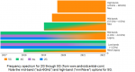
Simulation is woefully incomplete for this kind of checking; production methods depend instead on signoff through static analysis which is very complete but always plagued by a high-level of false errors. You want the analysis to err on the side of pessimism to avoid missing any real errors, but even a little pessimism quickly explodes into hundred of thousand of “possible” errors which you then have to check one by one. In practice many designers throw in the towel, checking the ran-the-tool box but ignoring the output. Or they use waivers to suppress major groups of violations, ignoring the possibility that one or two real problems may lurk under all that noise.
That’s a problem because, according to one speaker, that decision is invariably justified by this defense: “Look, this design/block has been in production for years and we haven’t seen any problems”. He made this point: failure rates on synchronizer cells can certainly be pretty long – that’s the whole point. But sync problems are not always point failures; they can also result from weak design practices at the block or system level. Not seeing any problems so far is no guarantee you won’t see problems in the future, given relentless growth in switchable power domains, clock domains or new use-cases triggered by different applications.
The real value in that reduction is often in isolating crossings triggered by quasi-static signals, which can change but don’t do so very often; resets and configuration signals are examples. Agreeing these few asserted properties are safe is much easier and can eliminate huge numbers of violations at a stroke. And the reasoning is way more robust than blanket waivers. Several speakers emphasized the importance of constraints over waivers for exactly this reason.
Checking reset domain crossings (RDCs) is becoming a big topic, quite closely related to CDC checking but different in some important ways. The need for analysis arises thanks to the increasingly complex hierarchy of resets in large chips, from basic power-on-reset through brown-out resets, to system and sub-system soft resets. Turns out there are many more crossings in a design – places a reset can interact with an async clock – than there are CDCs. So the false error problem has to be managed even more carefully
Ironically the RDC problem can arise in an attempt to resolve lockups in software (or hardware), especially now in fail-operational requirements in ISO 26262, where if a system fails in some respect it must be able to recover without requiring a complete reset. The design fix is to use local resets which if incorrectly implemented can cause their own sync problems.
One user observed that they currently do the reset check in STA, which works but pushes analysis late in design. If they need a fix, it becomes an ECO which can be very painful as these accumulate. Checking from RTL onwards and rechecking at every checkin, regression and checkpoint minimizes ECO surprises (at least from this cause).
Several other points of note: One user observed that they have been doing reset checks in STA, but that necessarily happens late in design. Given increasing complexity of reset hierarchies, these fixes trigger complex and hard to manage ECOs. Going forward, they’re switching to checks from RTL onward to minimize the need for late-stage fixes on resets. Also CDC signoff continues to be important at gate-level, thanks to all the changes that can happen in implementation – clock gating muxes transforming into glitching AOI structures if you’re not careful, synthesis retiming optimizations around synchronizers, you get the idea. Finally, hierarchical analysis is becoming much more important. Full-flat analysis on billion gate designs is as problematic for domain crossing analysis as for STA and everything else. Progress is being made; more is probably needed in the challenging area of abstraction.
You can learn more about Synopsys support in all these areas through the SpyGlass platform HERE.


