
ASML in line QTR with big Orders
Near term slippage w long term upside
Logic is strong but memory recovery unknown
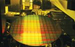
EUV is finally a reality/commercialized
In line quarter- supplier slippage expected in Q4
Results were revenues of Euro 3B and EPS of Euro 1.49, more or less in line with earnings estimate if a tad bit light in revenue. Outlook for Q4 is Euro 4B with 4 EUV systems slipping into 2020 due to supplier issues (now resolved)
Logic is leading the recovery… Obviously TSMC
Over 70% of orders are from foundry/logic customers as everyone is getting in the queue now that EUV is in commercial production. TSMC is the leader in real EUV and likely accounts for the largest portion of those future EUV orders
Memory still an unknown
Several months ago we said that the recovery would be led by logic as the memory recovery would take longer than most people expected due to the sidelined capacity amid excess supply and weak pricing.
This is becoming clearer to most people as we have heard from Micron, which was weaker than many expected and now clearly hearing from ASML that memory business remains weak with unknown timing of a recovery.
Some are expecting a recovery early in 2020, but we would not get our hopes up as it could take all of 2020 to get memory back on track.
Huge orders Euro 5B and 23 EUV tools
ASML is selling out its capacity very quickly as we are now seeing a virtual avalanche of orders. EUV has been proven and no customer wants to be excluded from the party or perhaps run out of capacity.
Part of the huge ramp is the large ramp in the numbers of layers in a chip made with EUV, going from a few ,like 3-5, going to 12 to 15 (depending upon whom you believe). Basically the number of tools has to increase proportionately with the number of layers. Memory is still a long way away from using EUV so in our view the current memory weakness, while impacting DUV and immersion is not slowing down EUV.
In a perverse way, the weakness in EUV demand for memory is likely of benefit to the logic side of the industry as it doesn’t compete for limited EUV tool availability.
40 plus EUV tools should be very easy to book for next year as we are more than halfway there. I think we can get there even without any memory recovery.
Not worried about supplier slippage
Given the complexity of an EUV tool and the huge supply chain we are certainly going to see issues here and there. The fact that its only a one quarter slip suggests its not a big or systemic problem.
We would likely take a longer term view as to the overall trend and worry less about the actual ship date and whether it falls within one quarter or another. ASML is not in a “turns” business like dep and etch or other relatively simple to assemble tools.
It down to production execution
As we are now past the milestone of actual commercial EUV production we are past the point of invention, luck, and pain and suffering trying to get the technology to work and more focused on production issues and the ramp of manufacturing.
To be sure, there are still many issues out there, pellicles, resist, reticle inspection, but what we have is working well enough to push forward on the number of layers using EUV and thus more tools.
We have covered ASML for almost 25 years with much of that history watching the EUV saga play out, so it is interesting to see the final conclusion (or perhaps beginning) of an era.
The stock –
Priced for perfection in an imperfect world, but still pretty good. ASML’s stock has steadily climbing based on the view of a recovering chip sector. Some stocks in the space have gotten a bit ahead of themselves but we think ASML’s value increase is justified given where we are with EUV, the strong logic/foundry demand and overall positioning in the market. Some investors may be unhappy with the slippage, but we are less concerned as you have to look at the longer term.
Some investors may be unhappy with a quarter that was just “in line” but given the memory weakness, we think “in line” is very good performance as ASML is working with one hand (memory) tied behind its back.
Overall we remain constructive on the stock and would look at pull backs or weakness as an opportunity to build or enhance a position going forward.
The stock is not cheap but the performance and positioning support the valuation.
We think that ASML has the lowest China/US trade problem exposure (though not zero) and EUV sales are less impacted by near term economic gyrations as the backlog is likely very strong. All in all a relatively defensive position in a very cyclical industry.
Summary
ASML remains a virtual monopoly, with a huge defensive moat, upside potential in revenues and margins and a leading technology position. We expect margins and therefore profitability to increase steadily as EUV ramps over the next few years leading to long term upside. It remains one of our top picks in large caps in the space.


