
In 1977 I made a job change: I took a job at Raytheon Semiconductor. Raytheon was on Ellis Street next door to the Fairchild “Rust Bucket”. In the early days, they shared the same parking lot so my commute didn’t change much, but my outlook on life changed a bunch. I had mostly enjoyed my days at Fairchild, but I hated every single day I spent at Raytheon.
Then, in 1979, I got a break! Gene Conner (a great boss and AMD’s first product engineer) offered me a job as product manager of AMD’s Interface product line. I jumped on it!!! Wow. It was like dying and going to heaven. Within a few days Gene taught me the most important thing that you had to understand if you were going to be a manager at AMD.
People first. Products and profits will follow.
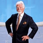
Jerry Sanders was definitely a flamboyant guy. Some of the stories you may have heard are probably overstated, but he was flamboyant! He was also very sensitive to the needs and feelings of the people who worked there. Jerry hated the idea of layoffs. Layoffs are very different from firings. Someone gets fired if they don’t do their job well. It seems harsh, but sometimes that has to happen. With layoffs, though, people who are doing their job well get let go. We all hate that. Jerry particularly hated it. Layoffs were a common part of the Silicon Valley culture at the time (See my week #7. Layoffs Ala Fairchild). Jerry didn’t want AMD to be like that. He instituted a no-layoff policy at AMD. At first it was an informal policy. Later, he had it written in the company’s policy manual. For 17 years he stuck to it. If things weren’t going well temporarily, Jerry’s view was – hold on to the people and let the earnings suffer. Not the other way around. That was unheard of in Silicon Valley semiconductor companies. It made people want to work at AMD. The great recession of 1984 came. We dropped into a loss position. Our spending was too high. Our sales too low. The cash balance wasn’t strong. At an executive staff meeting we were hashing out what we could do about it. The subject of a layoff came up. Several execs were pushing for a layoff. Jerry went apoplectic. He banged on the table yelling, “I’m not going to preside over the dismantling of my life’s work.” Jerry was always a good “quote machine”, but that one in particular will stick with me forever.
(Unfortunately, by the time 1986 rolled around we were still in a loss position and the cash balance was running dangerously low. We were forced to abandon the policy.)
In 1980 we had a very good year. Jerry wanted to spread the wealth. He decided to hold a raffle. The winner of the raffle was to get a house! Yes. The title to a real house here in Silicon Valley! Even back in 1980, production workers generally couldn’t afford their own houses. The raffle was held, as I recall, on a Saturday night. Early Sunday morning Jerry, accompanied by a Channel 7 TV crew, went to the home of the winner (A Fab worker named Jocelyn Lleno who didn’t have any idea that she had won) and knocked on the door. When she answered the door wearing her bathrobe, he told her, “Hi. I’m Jerry Sanders. I came here to tell you that you won the raffle. You’ve won a house here in Silicon Valley.” She was blown away!!! (Actually, the prize was $1000/month for 25 years. Hard to believe, but in those days that was enough to buy a very nice house)
Once at a black tie dinner event for AMD executives and their wives, I was assigned to sit next to Jerry at dinner. My wife Pam sat directly to his right. Jerry knew that Pam owned a dance studio (she still does). He asked her how the studio was going. It happened that Pam was about to take a contingent of dancers to Russia, Poland, and the Ukraine for three weeks as part of an exchange program – a cadre of Russian dancers had just visited Silicon Valley. It was expensive to take all those dancers to Russia and nobody had figured out how they were doing to pay for it. So Pam — extrovert that she is – responded with something like, “Well. I’ve got a problem. I don’t know how I’m going to pay for this Russian exchange. Can you help?” As I crawled out from under the table, I saw Jerry reach into his jacket pocket. He pulled out a check book and wrote out a personal check for $1000.
I first met TJ Rodgers in 1982 when he worked at AMD. Shortly after that, he left AMD to found Cypress Semiconductor. In 1992 plus or minus a year or two Valerie Rice, a writer for the San Jose Mercury News, was interviewing TJ. The fabless concept hadn’t yet taken over the world, but it was making inroads. Valerie asked TJ what he thought about the fabless model. I love TJ Rodgers! He was one of the old guard CEOs (As I was). He believed in Fabs, device physics, and transistor level circuit design (Things have changed. See my upcoming week #15. The Decade that changed the industry.) Valerie tried to help by summarizing what he had said. “So, you’re essentially saying that real men have fabs, right?” That was a play on the title of a book that was very popular back in the day. Real Men Don’t Eat Quiche. TJ jumped on it. “Exactly!!!” Jerry Sanders read that line and loved it! Later that year he was the lunch speaker at the Instat Conference (Jack Beedle’s annual semiconductor conference that was attended by virtually all the big brass in the business). The high point of his talk? In his very strongest “take charge of the room and lay down the law” style: “Now hear me and hear me well. Real Men Have Fabs!!!!” Most of the speakers that afternoon were fabless company CEOs. I was one of them. Jerry’s talk sent us all scurrying back to our power points to make the necessary changes. The Instat Conference was always fun, but that was the best one ever!!
There was something about the AMD environment that spawned CEOs. Was it the collegial environment? In total, 83 former AMDers have gone on to become CEOs of other tech companies. The two who impress me the most, though, are two CEOs who were just starting their careers at AMD during the days when I was a VP there. Jayshree Ullal and Jensen Huang. Jayshree (the CEO at Arista Networks) took Arista from a fledgling company to one now valued at twenty billion dollars! There’s a great article about her in Forbes Magazine. Jensen (the CEO of Nvidea) has built a juggernaut, but I think of him as the best public speaker I have ever listened to. (Actually – he’s tied with Jerry Sanders who is the greatest orator in the history of High Tech!!!). At the typical dinner event, most of us can’t wait until the keynote speaker shuts up so that we can eat. In the case of Jensen, though, you don’t want him to stop. He’s just plain fun to listen to.
There was a terrific amount of camaraderie and love for the company in the early days of AMD. A terrific spirit! It seemed to me that it waned a bit, though, when Jerry left. This May 8th I was invited to attend the AMD 50th birthday celebration in their new offices in Santa Clara. It was a really well planned event. I talked briefly with Lisa Su (The new CEO) and with a dozen or so of the present-day rank and file employees. My takeaway? Lisa Su is great and the spirit is back.
Jerry Sanders was CEO of AMD for 33 years. TJ Rodgers was CEO of Cypress for 33 years. The industry lost a lot when they retired! I miss them!!!
Next week: The IBM PC
See the entire John East series HERE.
Pictured: Jerry Sanders


