The next generation FPGAs have been announced, and they are BIG! Intel is shipping its Stratix 10 GX 10M FPGA, and Xilinx has announced its VU19P FPGA for general availability in the Fall of next year. The former is expected to support about 80M ASIC gates, and the latter about 50M ASIC gates. And, to bring this mind-boggling gate capacity into your prototyping lab immediately, S2C has teamed up with Intel and has rolled out its new 10M Logic System prototyping platform and will be delivering first systems before the end of this year.
On-Demand WEBINAR: Prototyping with Intel’s New 80M Gate FPGA and S2C!
You might ask: “How will this affect FPGA prototyping?”. Well, there are at least three ways you should expect to benefit from these larger FPGAs:
- More usable ASIC gates from a single FPGA.
- Higher prototype performance.
- Faster time-to-prototype.
More Usable ASIC Gates
For those of you gagging for more usable gates from a single FPGA, the 10M Logic System is an FPGA prototyping solution you can deploy today. One example of an application that will need increasingly more ASIC gates over the coming years is video processing. SoCs incorporating video blocks already exceed the gate capacity of the previous generation FPGAs, and designers are scrambling to keep up with today’s video features, with no end in sight of the addition of incremental new features. S2C’s 10M Logic System brings more than twice the usable gate capacity per FPGA to video applications today, and supports continued gate capacity growth with Dual and Quad FPGA versions available early next year.
Higher Prototype Performance
Another inherent benefit from these new, larger FPGAs is performance. The S10 GX 10M die core performance is rated at 900MHz, with LVDS I/O and single-ended I/O rated at 1.4GHz and 250MHz respectively. Actual prototyping performance will vary by application, but, with all other things being equal for a comparison, prototype performance will be higher with these new 14nm FPGAs.
Organizing the design hierarchy for prototyping to contain the high-performance block/signals within one FPGA will certainly lead to higher prototype performance. With S2C’s new 10M Logic Systems, design blocks up to about 80M gates can be contained within a single FPGA, and, for larger designs, Dual and Quad FPGA Logic Systems will include high-speed interconnects between the FPGAs.
The S10 10M Logic System supports six on-board programmable clocks (up to 350MHz), 5 external clocks, and an oscillator socket. Two dedicated programmable clocks are also provided for on-board DDR4 memories, as well as 2 global resets that can be sourced from an on-board push-button, an externally sourced reset through a connector, or under PlayerPro run-time software control.
Faster Time-to-Prototype
One of the keys to successful prototyping is minimizing “time-to-prototype”, and, fast time-to-prototype must consider:
- Getting your design running at your target speed on the FPGA prototype platform.
- A debug environment that enables high design visibility and deep test response data capture.
- A method for applying large quantities of high-speed test stimulus from a host computer or external source.
Getting your design running at your target speed in the FPGA prototype platform should include thoughtful preparation of the design netlist for FPGA implementation, while preserving correlation with the simulation netlist as much as possible. It should not come as a surprise to anyone that having a prototype team member with previous prototyping experience will go a long way to minimize time-to-prototype, especially when it comes to the FPGA implementation of design clocks and gated clocks, embedded memory, and SoC IP.
Since the simulation netlist is the verification “gold standard” that will be used for silicon tapeout, and FPGA prototyping should be viewed as a way to improve verification coverage beyond the capabilities of software simulation. Therefore, maintaining a correlation between the two netlists throughout the verification process is essential to overall verification productivity. If something goes wrong while verifying the design in the FPGA prototype, quickly diagnosing the cause of the problem in terms of the simulation netlist is what makes FPGA prototyping such a powerful verification tool. And, the importance to prototyping productivity of establishing and enforcing a strict discipline of bug tracking and netlist revisioning cannot be overemphasized for keeping the simulation team synchronized with the prototyping team.
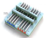
One approach to FPGA prototype debug with S2C’s 10M Logic System is to use S2C’s Multi-Debug-Module, or “MDM”. Set-up and runtime controls for MDM are integrated into S2C’s PlayerPro software, deigned to work with the 10M Logic System hardware, and allows test data from multiple FPGAs to be viewed within a single viewing window. MDM provides for up to 32K probes in eight groups of 4K probes without recompile. Trace data can be captured at speeds up to 80MHz, and up to 8GB of waveform data can be stored in MDM’s external hardware.
S2C Multi-Debug-Module
To assist in reducing time-to-prototype, S2C offers ProtoBridge for use with the 10M Logic System. ProtoBridge uses a PCIe/AXI high-throughput link between the prototype hardware and a host computer to transfer large amounts of transaction-level test data to the design. The test data width can be from 32 bits to 1,024 bits at data rates up to 1GB per second.
S2C ProtoBridge
On-Demand WEBINAR: Prototyping with Intel’s New 80M FPGA and S2C!
Also Read:
S2C Delivers FPGA Prototyping Solutions with the Industry’s Highest Capacity FPGA from Intel!
WEBNAR: How ASIC/SoC Rapid Prototyping Solutions Can Help You!