You are currently viewing SemiWiki as a guest which gives you limited access to the site. To view blog comments and experience other SemiWiki features you must be a registered member. Registration is fast, simple, and absolutely free so please, join our community today!
There is a live CEVA webinar coming up that you will NOT want to miss. We have been working with CEVA since 2012 and have posted 130 collaborative blogs. Those blogs have earned 927,901 views thus far and counting. The average blog on SemiWiki.com gets 5,885 views so they are ahead of the game.
One of the reasons CEVA is so popular on SemiWiki is due to the rising interest in commercial semiconductor IP from the electronics systems companies who are now doing their own chips. Another reason is that CEVA provides some of the best background materials we get on SemiWiki.
Additionally, CEVA is staffed by some of the smartest and most humble semiconductor professionals that we have the fortune to work with. A very good combination for a media portal partner, absolutely.
Robotics is a field that is growing rapidly. In particular, consumer ground-roving robots are becoming mainstream now that they commonly incorporate more intelligent navigation to operate more autonomously. Inertial measurement units (IMUs) are sensors that are essential for achieving precise navigation. IMUs can be used as a primary sensor for navigation or as a complementary sensor that helps VSLAM systems achieve robust performance. But making use of IMUs requires deep understanding of their idiosyncrasies and modeling to assess their impact. In this webinar, engineers will learn about the challenges when working with IMUs, how IMUs are applied in different robotics applications, and what is necessary to test IMU-based robots to achieve great performance.
Join CEVA’s experts to learn about:
Consumer Robot Vacuum Industry Overview
Common home robot navigation paradigms
Sensor idiosyncrasies and the importance of qualifying sensors
How to maintain accuracy over time, temperature, and environment
How to create robust algorithms and verify performance
Target Audience
Design, system, and product engineers looking to enhance their understanding of IMUs, sensor fusion, and how they relate to SLAM. Robot OEMs interested in navigation for their ground-roving robots.
Speakers
Charles Pao
Sr. Marketing Specialist, Sensor fusion BU, CEVA
Steve Scheirey
Sr. Director, Software, Sensor fusion BU, CEVA
About CEVA, Inc. CEVA is the leading licensor of wireless connectivity and smart sensing technologies. We offer Digital Signal Processors, AI processors, wireless platforms and complementary software for sensor fusion, image enhancement, computer vision, voice input and artificial intelligence, all of which are key enabling technologies for a smarter, connected world. We partner with semiconductor companies and OEMs worldwide to create power-efficient, intelligent and connected devices for a range of end markets, including mobile, consumer, automotive, robotics, industrial and IoT. Our ultra-low-power IPs include comprehensive DSP-based platforms for 5G baseband processing in mobile and infrastructure, advanced imaging and computer vision for any camera-enabled device and audio/voice/speech and ultra-low power always-on/sensing applications for multiple IoT markets. For sensor fusion, our Hillcrest Labs sensor processing technologies provide a broad range of sensor fusion software and IMU solutions for AR/VR, robotics, remote controls, and IoT. For artificial intelligence, we offer a family of AI processors capable of handling the complete gamut of neural network workloads, on-device. For wireless IoT, we offer the industry’s most widely adopted IPs for Bluetooth (low energy and dual mode), Wi-Fi 4/5/6 (802.11n/ac/ax) and NB-IoT. Visit us at www.ceva-dsp.com and follow us on Twitter, YouTube,Facebook, LinkedIn and Instagram.
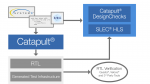
Formal verification has made significant inroads in RTL and gate-level verification because it provides complementary strengths to conventional dynamic verification methods; using both provides higher levels of coverage and confidence in the correctness of an implementation. I haven’t heard as much about formal use in high-level synthesis (HLS) flows so was interested to see a white paper from Renesas on how they use Catapult formal tools in this context.
First, why even use formal in such a flow? One reason is obvious. When you synthesize from one format to another, from C++ to RTL or from RTL to gates, no amount of simulation is going to prove conclusively that synthesis didn’t introduce some subtle error along the way. That’s why equivalence checking was invented, to prove that at minimum the input and output implementations are functionally equivalent at a cycle-level.
Another reason is to do some level of formal checking on the C++ itself. A couple of examples are out-of-range-accesses on arrays and uninitialized memory reads. You might catch these in C++ simulation, but you might not. Experienced programmers know that behind rarely taken branches can lurk dragons; formal is a good way to expose such problems. And the beauty of these methods is that they not only discover that a problem is possible, but they also show you how to create that problem, which should make it easier to figure out a fix.
Still, the bulk of Renesas’ usage is in equivalence checking and this starts with C++ to C++ checks. Renesas talks about image processing IP and communication IP, both natural applications for HLS. Both types of design are intrinsically complex and will evolve through multiple iterations. Equivalence checking between C++ revs can assure as completely as possible that unintended functional changes are not introduced.
This is sequential equivalence checking and will not always get to a proof of equivalence (or no-equivalence) without a little assistance. What will push a proof towards convergence in these cases is more hints (constraints) on behavior, such as bounding the range of an apparently unbound array index.
The best-known application of equivalence checking in HLS flows is in comparing the source C++ with the synthesized RTL. There’s an advantage here (I’m guessing) in having the HLS synthesizer and the SLEC equivalence checker come from the same product group. The checker knows what kinds of transformations the synthesizer can make, such as how it inserts pipeline stages, and can factor these in when looking for a complete proof.
I believe based on my reading of the Renesas white paper that they only edit the source C++, so all RTL changes are based on re-synthesis from source updates. They run equivalence checking on each RTL drop to establish either that they can get to a full proof or to find any bottlenecks to getting to proofs. This is with the goal of ensuring a full proof by the time they get to the final RTL drop.
Methods to help along full-proofs at this level are pretty familiar – help in identifying equivalence points between the two designs, along with some level of abstraction and hierarchical proving.
Renesas results are impressive in comparison with verification through extensive simulation. They show one example, for an image processor IP, in which they were able to reduce turnaround time from 260 days (simulation-based) to 4 days using equivalence checking. Of course you still want to do lots and lots of simulation (in C+) to prove functionality and performance. Catapult SLEC removes the need to worry about implementation bugs being introduced in mapping from C++ to RTL.
Qualcomm today announced three new chipsets for entry level and mid-range smartphones – Snapdragon 720G, Snapdragon 662, and Snapdragon 460. The first one promises to bring many of the Elite Gaming features of the 765G with support for HDR, dynamic color range and high-quality synchronized sound with Qualcomm aptX Adaptive.
The SD662 will bring triple-camera support, which is a first for a Qualcomm 6-series chipset. Snapdragon 460 might be most affordable of all three, but still will be able to provide an increase in CPU and GPU performance over other 4-series chipsets.
According to Rajen Vagadia, president of Qualcomm India, the chip maker is introducing these three platforms for 4G markets where seamless connectivity access is still unraveling. Kedar Kondap from the product management team of the San Diego company confirmed the 720G, 662, and 460 will be able to provide gaming experience at a more affordable price.
Senior executives of smartphone companies such as Manu Kumar Jain at Xiaomi and Madhav Sheth at Realme confirmed they will “work closely” with Qualcomm to introduce phones with the new chips, including the most interesting of all three – Snapdragon 720G.
Snapdragon 460 (11nm)
Key features:
CPU – 8x Kryo 240 cores up to 2.3GHz
GPU – Adreno 610 GPU
DSP – Hexagon 683 with vector extensions, hardware-accelerated TensorFlow Lite
ISP – Spectra 340 ISP supporting 25MP camera, or dual 16MP camera
Connectivity
Cellular – Snapdragon X11 LTE modem
WiFi 6 ready
Bluetooth 5.1 with advanced audio via the Qualcomm FastConnect 6100 platform
GNSS – Dual-Frequency (L1 and L5) GNSS for GPS, Galileo, GLONASS, Beidou, NavIC
Quick Charge 3.0 – 0 to 50% in 20 minutes
Process – 11nm
Snapdragon 460 is an update to the Arm Cortex-A53 based Snapdragon 450 processor with the custom Kryo 240 processor delivering up to 60% extra performance, while Adreno 610 GPU delivers up to 70% performance increase over Adreno 506.
Snapdragon 662 (11nm)
Highlights:
CPU – Octa-core “Kryo 260” processor with four Cortex-A73 cores @ up to 2.0 GHz, and four Cortex-A53 cores @ up to 1.8 GHz
GPU – Adreno 610 GPU
DSP – Hexagon 683 with vector extensions, hardware-accelerated TensorFlow Lite
Bluetooth 5.1 with advanced audio via the Qualcomm FastConnect 6100 platform
GNSS – Dual-Frequency (L1 and L5) GNSS for GPS, Galileo, GLONASS, Beidou, NavIC
Quick Charge 3.0 – 0 to 50% in 20 minutes
Process – 11nm
Snapdragon 662 looks very similar to Snapdragon 665, but with a slower modem, and better ISP. It also shares many features of Snapdragon 460, but with more powerful Cortex-A73 CPU cores, and better camera support.
Snapdragon 720G (8nm)
Key features and specifications:
CPU – Octa-core “Kryo 465” processor with 2x Cortex-A76 cores @ up to 2.3 GHz, and 6x Cortex-A55 cores @ up to 1.8 GHz
GPU – Adreno 618 GPU
DSP – Hexagon 692 Hexagon Tensor Accelerator
ISP – Spectra 350L ISP supporting 192MP cameras, HEIF capture, and 4K video capture
Connectivity
Cellular – Snapdragon X15 LTE modem
WiFi 6 ready
Bluetooth 5.1 with advanced audio via the Qualcomm FastConnect 6200 platform
GNSS – Dual-Frequency (L1 and L5) GNSS for GPS, Galileo, GLONASS, Beidou, NavIC
Fast Charging – Quick Charge 4+ allowing 0 to 50% charge in less than 15 minutes; USB PD support
Process – 8nm
Snapdragon 720G looks to be an upgrade to Snapdragon 712 with the processor delivering a 60% performance increase, and the GPU providing 75% better improve and support for HDR video playback.
Availability
Snapdragon 720G based phones will come to market soon as the first devices are slated for Q1 2020, but we’ll need to wait a little longer for Snapdragon 662 and Snapdragon 460 based smartphones which are scheduled for the end of 2020
Imec is one of the premier semiconductor research organizations and at IEDM they presented dozens of papers. I had the opportunity to see several of the papers presented and interview 3 of Imec’s researchers.
Jan Van Houdt, DMTS ferroelectric and exploratory memory
I have had very interesting discussions with Imec researchers about memory trends in the past and I asked to interview an Imec memory expert at IEDM this year. Jan Van Houdt has been Imec’s chief scientist and is now DMTS ferroelectric and exploratory memory. My interview with him wasn’t so much tied to specific Imec papers but rather a general discussion of the state of memory.
DRAM scaling has slowed and is facing very difficult issues. Last year at IEDM Imec presented work on Strontium Titanite (STO) dielectric for DRAM with higher K values that could potentially enable capacitor shrinks. He said they still hadn’t met all the specifications for k value, thickness and leakage and they are still trying to add elements to the films to address this. I asked him what he thought would be the long-term replacement for DRAM and he said they thought they could get Ferroelectric based memories to cost and density parity with DRAM but endurance is the key limiter. I was surprised by this, I thought Ferroelectric based memories were really just a niche memory but he was very optimistic about the future of Ferroelectric memories and that is why he has made it his focus. The current Ferroelectric material of choice is HfZrO4 with an endurance of 1E11 cycles.
Authors notes, DRAM replacement endurance needs to be >1E15 cycles. Of the current emerging memory types only MRAM and Ferroelectric have good endurance, PCRAM and RRAM are <1E8 cycles. MRAM can potentially have very good endurance but the high switching current requires large selector transistors limiting scaling.
If Ferroelectric can’t replace DRAM as main memory it could be a storage class memory option. He noted that 3D XPoint, a current storage class memory option is too expensive for the performance it offers.
With respect to 3D NAND scaling he mentioned that as the number of layers increases in 3D NAND memory, that the channel resistance becomes an issue. Imec has previously presented work on InGaAs as an alternative to the current polysilicon channels to provide lower resistance. In the original work the InGaAs was in direct contact with the ONO (Oxide-Nitride-Oxide) layer and had a bad interface. They are trying high pressure anneals and looking at ALD deposition. Ideally, they want to use ALD to deposit a crystalline channel. There is currently work being done in the industry to provide a crystalline silicon channel in place of the polycrystalline channel, with epitaxial growth or recrystallization being investigated. To-date epitaxial growth is too slow and expensive and NiSi recrystallization is slow and the Ni stays in the wafer.
There is also a lot of work being done to replace the W word line material in 3D NAND with a lower resistance alternative. They are looking at TiN to fix the channel work function and then Ru fill or Ru without TiN, Mo is also on the list. The switch to an alternate material will be driven by the need to reduce the layer thickness.
Authors note, as an expert in fabrication costs I think Ru will be much too expensive to implement in 3D NAND especially since the deposition is surface area driven and the surface area with a hundred or more word line slots to fill is very high and drives a lot of precursor consumption.
Imec has completed their work on STT MRAM and they are now focused on SOT MRAM using VCMA – Voltage Controlled Magnetic Anisotropy to switch without current. STT must run current through the Magnetic Tunnel Junction (MTJ) for reading and writing. SOT has no current through MTJ, you run the current near it to write but still need to run current through the MTJ to read it. SOT is a three terminal device, so bigger but can switch in 300 picosecond giving SRAM speed. They don’t have the endurance yet; it is early to talk reliability. In theory should be better than STT, STT is 1E10 to 1E12 but some bits fail earlier.
In Ferroelectrics they can do a FET that is a NAND cell and can provide thinner layers for 3D NAND. With InGaXOx they can do a 2T1C (2 transistor – 1 capacitor) memory cell for DRAM like memory, it has a very small capacitor because it is amplified can be in the Back End Of Line (BEOL). They can also try 1T1C (current DRAM standard) or 2T0C and use a parasitic capacitance. He thinks 2T1C is the most interesting.
Christopher Wilson, manager, nano interconnect program and BEOL integration
In this interview we discussed the paper: “Three-Layer BEOL Process Integration with Supervia and Self-Aligned-Block Options for the 3 nm Node”
This paper is an extension of work presented at the IITC conference where they showed 2-layer Ru with metal 2 at a 21nm pitch, the new work adds a 3rd metal layer. In order to achieve a 21nm pitch you need 2 block masks and they used self-aligned block. This work was done on a SRAM so it has a regular layout. The addition of metal 3 allows them to look at stacked vias. Landing via 2 on metal 2 is normally a critical design rule for Cu, the yield didn’t change much with island size. With 3 layers they can also look at super vias with a via from M3 to M1. Authors note super vias are when vias skip metal layers so instead of connecting metal n to metal n-1 you can connect to n-2, n-3 or more.
This paper was all based on ALD deposition of Ru, Co CVD deposition showed gaps. They have newer data on CVD of Ru but this is all ALD based. The ALD Ru deps were 3 hours per wafers and topped with PVD so a CVD or faster ALD deposition will be needed for production.
One important layout dimension in routing is the metal line tip to tip dimension that you want as small as possible. For Cu typically tip to tip is the same as the pitch so for a 21nm pitch, the tip to tip would be 21nm. In the paper they show no change in yield for a tip to tip of 18nm versus a tip to tip of 9nm and the 9nm is actually around 5nm. Ru has 30% better RC (Resistance-Capacitance) than Cu at these pitches.
For M3 the pitch is 36nm and that shows a 10x RC improvment versus M2 at 21nm.
Naoto Horiguchi, Director of CMOS device technology
In this interview we discussed four Imec papers.
First up was “Novel forksheet device architecture as ultimate logic scaling device towards 2nm”
The forksheet is a advanced version of a horizontal nanosheet (HNS) where a dielectric sheet is placed between the nFET and pFET. Because of how HNS are fabricated they can end up with a larger n to p spacing than a FinFET. The additional of the dielectric wall acts as an etch stop layer. Figure 1 illustrates the effect of n to p spacing on standard cell size.
Figure 1. N to P spacing effect on standard cell size.
Figure 2 illustrates how a dielectric wall in a forksheet mitigates the n to p spacing.
Figure 2. Forksheet dielectric wall mitigates n to p spacing issues.
A forksheet is essentially a FinFET rotated 90 degrees so the electrostatic are not as good as a standard HNS. Recessing the channel during dielectric wall formation can help recover some electrostatic performance. The dielectric wall reduces miller capacitance and can yield 10% higher speed or 24% lower power.
N to p boundary is typically 2x the Fin pitch, the dielectric wall reduces this. For example a 5 track height cell can be reduced to a 4.3 track height cell with the dielectric wall, see figure 3.
Figure 3. Cell scaling advantage for forksheet with dielectric wall.
He believes that the forksheet provides a minimum 20% area improvement.
The second paper we discussed was: “Variability sources in nanoscale bulk FinFETs and TiTaN- a
promising low variability WFM for 7/5nm CMOS nodes”
TiTaN si a potential work function material for controlling threshold voltages (Vt). They deposited it on a high-k dielectric and compared it to TiN and TiN with a SiH4 soak. The SiH4 soak of TiN kind of dopes some silicon atoms on the surface and reduces crystallization improving variability and Vt shift. TiTaN showed a significant further reduction in variability, it is a more amorphous material. TiTaN can be deposited by ALD and can be used on n or p although on p a TaN barrier is needed to block from TiAl.
The third paper we discussed was: “3D-carrier Profiling and Parasitic Resistance Analysis in NW h-GAA CMOS Transistors”
In this work a diamond tipped atomic force microscope is as a scalpel to remove material while also running a spreading resistance probe and create a 3D map of conductivity.
What was found is that dopant diffusion is slow in HNS at the S-SiGe interface.
Authors note, HNS are fabricated as alternating layers of Si and SiGe where the SiGe is a sacrificial layer that gets removed later.
This reduced diffusivity effect will become more important as devices scale and it can impact interface resistance. The ability to measure conductivity at a nanoscale enable better modeling and fundamental understand for future device development.
The final paper we discussed was: “Vertical Nanowire and Nanosheet FETs: Device Features, Novel Schemes for Improved Process Control and Enhanced Mobility, Potential for Faster & More Energy Efficient Circuits”
Vertical nanowires (VFET) are very good for regular layouts such as SRAM or MRAM selectors but not as good as HNS for random logic. This work continues previous Imec work on these devices to further refine the fabrication and performance.
In this work a sacrificial SiGe sleeve is used to introduce stress, the sleeve is fabricated introducing stress and then later removed. This work also showed improved alignment control with a partially self-aligned technique using spacers.
This work could be very interesting for fabrication of highly optimized SRAM chiplets to integrate with logic using 3D packaging techniques. I also found the MRAM selector option very interesting. As I mentioned earlier in this article MRAM selector size is relatively large and limits MRAM scaling. Figure 4 illustrates density improvements by using VFET versus a FinFET.
Figure 4. VFET MRAM selector area advantage versus FinFET.
Conclusion
Imec continues to be a premier research organization in Semiconductor devices and process technology. Innovations such as VFET and Forksheet HNS provide promising options for future scaling. More fundamental work such as understanding carrier profiles in 3D and new work function materials are also key enablers.
After returning from a week in Southern China I found the TSMC Q4 2019 conference call even more interesting. In China they are preparing for the New Year’s Celebration so everything is very festive but what struck me hardest was the massive investment in infrastructure and security. Semiconductors are of course a big part of that thus the urgent need for China to be semiconductor-self-sufficient, absolutely.
TSMC of course is a valued partner of China and will benefit the most from China’s continued semiconductor boom. If you read between the lines of the TSMC Q4 conference call you will see it more clearly. First let’s look at the technology parts of the prepared statement:
“16-nanometer and below, accounted for 56% of wafer revenue, up from 51% in the third quarter. On a full year basis, 7-nanometer contribution increased from 9% in 2018 to 27% of wafer revenue in 2019. 10-nanometer was 3% and 16-nanometer was 20%. Advanced technologies accounted for 50% of total wafer revenue, up from 41% in 2018.”
It is interesting to note that TSMC 20nm and 16nm shared fabs where 20nm was the sacrificial lamb and 16nm is the cash cow. It was the same with 10nm and 7nm (cash cow). So, what is going to happen now that TSMC is moving 7nm customers to 6nm and 5nm is ramping up this year? Will TSMC break the cycle and have two cash cows in a row? From what I have been told 6nm is an EXCELLENT process and will be VERY competitive on price / performance with both TSMC and Samsung 5nm. In fact, my guess is that TSMC 6nm will even outperform Intel 10nm on density, yield, and most certainly cost.
“Now let’s take a look at revenue contribution by platform…. On a full year basis, smartphone and IoT led the growth with 12% and 33%, respectively, while HPC, automotive and DCE decreased 8%, 7% and 8%, respectively… Overall, smartphone accounted for 49% of our 2019 revenue; HPC, 30%; and IoT, 8%.”
Remember, in 2019 China is second in TSMC revenue (20%) behind the US (60%) but well in front of the other parts of the world and China revenue is on the rise. My guess is that China will be 25% of TSMC’s revenue in 2020 further out pacing Japan, Korea, Taiwan, and the EU, who are all in single digits.
The TSMC smartphone and IoT surge are a very good reflection of the China market.
Samsung is being pushed out of china leaving Apple as the only foreign smartphone supplier in the top 5. Huawei is dominating and Huawei and TSMC go together like peanut butter and jelly. In order to compete the other China smartphone suppliers are forced to follow Huawei into the TSMC ecosystem so it is all about TSMC.
IoT is the interesting one. The number one IoT driver in China is security (cameras) which are EVERYWHERE and backed by AI. 5G is a national priority in China and will increase the abilities of AI on the edge.
For example, in the US we have license plate readers so our local police can identify and recover stolen cars and the criminals that are driving them. The next level is facial recognition where law enforcement can identify known criminals and recover them. China is already at that next level, semiconductors and AI are everywhere and there is no stopping it no matter how you feel about privacy.
“We raised our 2019 CapEx guidance by $4 billion to $14 billion to $15 billion, and we ended up spending $14.9 billion. Our 2020 capital budget is expected to be between $15 billion and $16 billion. Out of the $15 billion to $16 billion CapEx for 2020, about 80% of the capital budget will be allocated for advanced process technologies including 3, 5 and 7-nanometers, about 10% will be spent for advanced packaging and mask-making and about 10% for specialty technologies.”
As I mentioned before, TSMC won the 7nm, 6nm, and 5nm popular vote so do not be surprised if CapEx is again raised and we have another hockey stick of growth in Q4.
“For the full year of 2020, we forecast the overall semiconductor market growth excluding memory to be 8%, while foundry industry growth is forecast to be about 17%. For TSMC, we are confident we can outperform the foundry revenue growth by several percentage points in U.S. dollar term.”
Now that ‘s what I’m talking about… 20% growth. It really is satisfying when hard work pays off.
“Now allow me to talk about our N5 volume production. Our N5 technology is a full node stride from our N7, with 80% logic density gain and about a 20% speed gain compared with 7-nanometer. N5 will adopt EUV extensively and is well on track for volume production in first half this year and with good yield.”
“Finally, I’ll talk about our N3 status. We are working with customers on N3’s design, and the technology development progress is going well. We have many technology options in development and we carefully evaluate all the different approaches. Our decision is based on technology, maturity, performance and cost… We will announce more details about our N3 technology at our TSMC North America Technology Symposium on April 29.“
TSMC N3 will again be FinFET based. We can talk more about this after the Symposium. The Q&A was pretty lame this time but here is the best answer:
“But I can just tell you that whatever you read on the newspaper is not true…”
In a week where the “phase 1” trade deal between US and China was finally signed, here is all the key news from the semiconductor and technology sector around the world.
Just as important as what is in the phase 1 deal are the items that are left out and are the major items to negotiated for the next phase. This BBC article reviews the major items missing which include the issue of China subsidies to companies in of support it’s “Made in China 2025” policy. Also excluded is the ban on Huawei and further reductions in tariffs that still remain. Let’s hope that progress is made on these more difficult items soon.
According to Gartner, last year Intel regained the number 1 slot for semiconductor companies based on global revenue in 2019 as Samsung dropped to number 2 due to the decline in memory prices and sales in 2019. Overall Global semiconductor revenue dropped 11.9% in 2019 compared to a year ago according to Gartner.
This optimism is backed up by initial trade data from Korea, where Korean semiconductor exports rose 12% in the first 10 days of 2020 in a sign that the industry is recovering from the negative effects of the trade war. This is the first time the figures have shown growth since October 2018.
TSMC expects to post revenues of between US$10.2 billion and US$10.3 billion in the first quarter of 2020, representing a 1.4% sequential decrease, but up a massive 44% on a year ago. TSMC also set its capex target this year at between US$15 ~16 billion, up from the US$14.9 billion allocated in 2019 with the majority of capex to be spent on advanced process nodes including 7nm, 5nm and 3nm. TSMC’s Q4 revenue increased to US$10.4bn, up 10.6% sequentially of which 7nm chip shipments accounted for 35% of its total wafer revenues, up from 27% in the prior quarter. Advanced technologies, defined as 16nm and below, accounted for 56% of TSMC’s total wafer sales. In Q4 2019 smartphone revenues accounted for 53% of TSMC’s total wafer revenues, followed by the HPC segment with 29%, IoT with 8%, automotive 4% and digital consumer electronics 3%. In terms of markets, North America remained TSMC’s largest market with a 59% revenue share in Q4 whilst China accounted for 22%. This is up 9% compared to the same period in 2018. With business booming, according to Digitimes, TSMC 7nm process lead time remains at about six months, with tight supply expected to last through 2020
My friends at McKinsey just released their annual look at the Chinese consumer. As always, they have interviewed thousands across China to draw out “what is different this year?” They start however from the key point that has not changed – that over the 2000s China has accounted for almost one third of the growth in global household consumption. And so, China ends the decade with a consuming middle class, hundreds of millions larger than it started the decade with.
Each of the 5 snapshot conclusions drawn from the survey can benefit from being put in the context of broader trends of the decade, which is what I try to do briefly below using my own personal experiences:
Growth from younger consumers in lower tier cities
Almost every consumer-focused company selling products – beverages, clothing, electronics – or services such as food delivery, travel, education – knows that they need to build reach in third and fourth tier cities. It is simple maths. What has surprised some is the bias of youth in these cities to spend on services rather than stuff, and on their willingness to spend at rates that it seems their income levels could not support. There are 2 reasons for this. Firstly, this generation is less enamored of the save to buy a property life style choice that the previous generation made. This generation is becoming accepting of the less cash demanding approach of renting. They are also much less interested in buying cars, ride sharing is their preferred way of getting around. And when cash flow runs short this generation is the most willing ever in China to spend on credit, to buy on installment. Their leverage is on average still supportable but is rising fast. Larger numbers will hit spending limits over the next couple of years.
Consumers becoming smarter in their spending
The report divides consumers into various segments, largely based on income and on how busy their lifestyles are. The trend of consumers across the board to place greater value on their time is one of the most fundamental changes over the last decade. Enabled by technology, Chinese consumers expect now to never have to wait in line, to check in, to use their bank, to pay at the store, to deal with government services. Recognize my face or my phone, listen to my voice and give me what I want, now. Any company that cannot deliver on this will be consigned to history as fast as the lines at the bank have disappeared. Chinese consumers now look to free up even more time – the replacement of cooking at home with delivery, of going to the store with home delivery and more.
The reminder from the report that the lower income segment still exists and that they want inexpensive products is important. It is too easy to get sucked into the narrative that all consumers are trading up. As the users of Pinduoduo prove, many remain in the “just getting by” category of spenders for whom cost remains paramount.
Health concerns shape more and more of consumer spending
Many, many categories benefit from this trend. Food suppliers using blockchain to prove to consumers the origin and path to plate of foods they are buying. Food suppliers providing more information on their packaging. Food suppliers offering more plant protein alternatives to meats, the source of which is not trusted. Growing cross border imports of food, supplements, vitamins, and pharmaceuticals. Air and water purifiers in the home, office, and car. An explosion of innovation in health insurance products, often linked to the application of technology to personal health tracking. Gyms and other forms of exercise. Companies should seek out and embrace the health-related aspects of their products and services, a potential source of differentiation.
Consumers becoming more sophisticated travelers
Anyone who travels to and from China experiences the spectrum of Chinese tourists – the tour groups of first-time travelers at the back of the plane heading to Bangkok, and the individual family groups at the front of the plane ticking off their third safari destination in southern Africa. Businesses and destinations have to adapt both to the needs of these distinct traveler groups and their numbers. Across China and in many international destinations, popular sites are simply swamped, creating unpleasant experiences and in worst cases safety hazards. Chinese travelers are incredibly sensitive to the perceived risk of travelling. An accident involving Chinese tourists on a boat off Phuket leads to millions fewer visiting Thailand in the following years. For many reasons, but with safety concerns prominent among them, Chinese tourism to Hong Kong is currently down over 90%. At a smaller scale an incident in a hotel where a Chinese tourist reports being badly treated following a theft could lead to a full boycott of the hotel, enabled by WeChat. Chinese tourists are also very sensitive to political winds, if government to government relations with a specific country are poor, Chinese travelers will tend to stay away.
The proximity of the Tokyo Olympics to China will mean that millions of Chinese travelers from the most to least experienced will visit Japan in August 2020. It will be interesting to see if their experience meets their expectations.
Rise of Chinese brands
The rise of Chinese brands in many categories reflects as much as anything the rise in capabilities of the Chinese companies that own these brands. Their growing depth in product development for China specific products, in the intricacies of marketing to Chinese consumers, in supply chain management and more has not just allowed Chinese companies to catch up with their global peers.
Generally, Chinese consumers are buying these products because they prefer them based on the essential characteristics of the product, not because the brand wraps itself in the flag and growing online nationalist tendencies. The one major exception to that is in technology where, with government encouragement, Chinese companies do emphasize their nationality as an important reason for consumers to buy their products. Companies should be alert to this behavior seeping into other sectors.
Closing
What is not in the report this year? There is, surprisingly to me, very little on the impact of an aging China or on the spending patterns of the retired. China’s cities have very varied proportions of young and old. Growth in consumption is going to be skewed to those, like Shenzhen, with the youngest age profile. Is spending by the elderly holding up as they head into retirement and their incomes fall? Is healthcare already consuming their discretionary cash – a recent Chinese government projection forecast spending on this to rise to over 25% of GDP by 2050.
There is a temptation to blame U.S. President Donald J. Trump for everything that is right or for everything that is wrong in the world today. Either that or blame Brexit. It’s just possible that Uber, instead, ought to be considered the target of shame for everything from traffic fatalities to global warming.
The automotive industry is in the midst of an extended sales swoon not attributable to any single obvious global economic downturn. There is a tendency to blame Trump trade tensions for the slide. A more obvious culprit is the emergence of ride hailing which has introduced billions of dollars in cheap, subsidized transportation across the developed and developing world.
Regionally, the auto industry is being hit hardest by the auto sales downturn in Asia, a region which previously delivered the lion’s share of industry growth. It should come as no surprise, then, that Asia has rapidly become the epicenter of the ride hailing phenomenon.
Uber and Lyft and Yandex and Gett may be popular in their respective geographies, but the tsunami of subsidized ride hailing availability in countries such as China and regions such as Southeast Asia (Grab and Gojek) is orders of magnitude beyond the growth rates in more developed markets. China alone dominates the landscape of ride hailing availability and usage.
SOURCE: Strategy Analytics
Strategy Analytics estimates the number of ride hailing drivers – working for operators such as DiDi Chuxing – in China at more than 19M by the end of 2019. The number of users in China, alone, is in the hundreds of millions.
Taxis were already cheap in China. But ride hailing operators can be cheaper still and introduce a new level of convenience for payment and pickup.
Factor in the high cost, complexity, and inconvenience of acquiring a license plate – let alone an actual car – in China, and a clear picture emerges of vastly simplified consumer decision making as regards owning a vehicle or using ride hailing. Perhaps more than in any other market, driving for DiDi may be the shortest path to obtaining a vehicle in China – other than purchasing.
This phenomenon is operative elsewhere in the world. Uber has been blamed for undermining the profitability of prominent car makers such as Ford and General Motors in Brazil, where cars are increasingly being leased by ride hail drivers from rental car operators that purchase vehicle at bulk discounts.
According to a Reuters report, Uber and DiDi encourage the rental car operators to buy cars to be leased to drivers thereby increasing their purchasing leverage with the auto makers. Of course, this has driven up the number of ride hail vehicles on the road – comparable to the run up in China – more drivers, more passengers. (Reuters quoted Anfavea consumer car buying research in Brazil showing the availability of Uber and DiDi as the second most reported reason for avoiding a vehicle purchase – after financial limitations.)
Of course, Brazil (Uber’s second largest market) and other South American countries, may face a reckoning as a surplus of drivers may cause Uber and DiDi to reduce driver incentives. Such actions in China, reported by Bernstein & Associates, produced a fourth quarter 2019 downturn in the number of drivers and passengers.
It is worth noting this ride hailing dialectic, given Uber’s early claims that the service would devastate or eliminate car ownership altogether. At the outset of ride hailing, consumers shift away from owning cars in favor of using Uber et. al. Uber et. al. commence aggressive advertising and recruiting of drivers – including those that do not own cars thereby creating a market for rented/leased cars.
Uber et. al. cut deals with car rental companies to expand their fleets – this “artificially” inflates vehicle demand. Fleets of vehicles sponsored by Uber et. al. add to traffic and congestion. Uber et. al. supply begins to exceed demand, and Uber et. al. begin to reduce incentives thereby puncturing the demand bubble of their own creation.
DiDi’s reported pullback on incentives in China likely reflected a diminishing supply of investment capital, according to analysts. In fact, multiple reports indicate Softbank is pulling in the reins on its investment targets including organizations ranging from WeWork to peer-to-peer car share operator Getaround and car subscription provider Fair.
Where regulators have been shy to step in, capital markets may end up limiting what has ‘til now been unbridled growth in the ride hailing sector. Uber, DiDi, Yandex, Gett, and others have increasingly been blamed for increased congestion, vehicle emissions, and even highway fatalities. Every discounted and subsidized Uber ride is arguably an avoidable contribution to global warming, right?
As cheap capital dries up, however, cheap rides too may become a thing of the past. The decline in cheap rides will, in turn, contribute to the expected recovery in vehicle sales and ownership. One thing seems clear, Trump, alone, cannot be blamed for the current downturn in vehicle sales, and increasing highway congestion, emissions, and fatalities. As for global warming, we can say Trump shares blame with Uber and DiDi and the rest. In reality, we are all to blame as the demand for automobile ownership remains high – reflected in forecasted increases in vehicle sales in the years ahead.
Samsung is warming up and spending again
Samsung gave its preliminary report for Q4 and it was well better than prior muted expectations. It doesn’t take long for Samsung’s business units to respond to business trends in either direction and we have already heard of increased spending plans on the part of Samsung.
Samsung has not been shy about spending and has even spent to excess as 2018 bore out. Samsung is equally not shy about cutting spending when the industry slows. We have heard that Samsung has already started to spend even though the recovery in memory is still in early stages and DRAM is well behind NAND in terms of a recovery.
Obviously this is the Wayne Gretzky philosophy of “skate to where the puck is going, not where it has been”. Samsung is trying to get out in front of an expected memory uptick.
This is despite the fact that we have a ton of excess capacity in idled tools sitting around waiting to be turned back on which could easily satisfy increasing demand.
We think that part of Samsung’s spend is more focused on technology rather than pure capacity spend. Samsung has always tried to best its competitors by staying ahead of the cost/technology curve and one way to lead the way out of the memory slow down would be to have an ability to make money at pricing levels that competitors lose money at.
We certainly don’t expect the “drunken sailor” level of spend that Samsung exhibited in 2018 but rather more focused and cautious spend with a technology leaning.
Will Samsung’s spend offset an eventual TSMC decline? As we have previously mentioned, many times, TSMC is a “seasonal” spender focused on getting to the next node in time for Apple’s fall launch of new Iphones. This means that new tools an technology gets ordered and shipped in Q4 and Q1 to iron out the process in Q2 and ramp production in Q3 for the fall launch. We are currently in the midst of a big seasonal spend cycle for TSMC getting its 5NM act together. It is TSMC’s Q4 spend hockey stick that has gotten the equipment industry off the bottom of the cycle.
But all good things come to an end in this most cyclical of industries and TSMC’s spend will likely slow a bit after Q1 as it focuses its efforts on ramping up all that shiny new equipment for 5NM. The real question is will Samsung’s spending ramp offset the expected slowing of TSMC? Probably yes…
We also expect a bit of share shift as memory based spend is obviously very different from logic/foundry spend.
BIS – Little known government agency may prove impactfull
Most people don’t know who or what BIS is. It is a government agency whose acronym BIS stands for “Bureau of Industry & Security”.
With the recent revelation about behind the scenes US pressure on ASML it is clear the government is using an old tool to combat China in the semiconductor industry and that is “national security”.
Its clear that the trade deal has little to no IP protection in it so other means will have to be used to limit the technology flow.
We have suggested that we will likely see more involvement from the government in the form of export licenses/export controls and other methods that are not tariff based.
The mission statement of BIS- “Advance U.S. national security, foreign policy, and economic objectives by ensuring an effective export control and treaty compliance system and promoting continued U.S. strategic technology leadership.”- seems tailor made to be an alternative method to achieve goals that the trade deal didn’t.
We expect to hear more from companies over the next few quarters as the government gets more involved in the regulatory side of trade with China, especially, obviously, in tech.
With think ASML is both the tip of the iceberg and beginning of new phase of government involvement.
While we don’t expect an embargo, we could easily see more scrutiny, more export license issues, denial of export licenses or delays that may impact tech exports to China without an “overt” action.
What will companies report about Q4?
We think companies will generally be more positive. Reports of end product sales have been good. CES 2020 has been very positive and trade concerns have fallen by the wayside.
Memory is getting better. Tech stocks are doing great. Everything is happy. This is all despite the fact that we are going into a seasonally weak Q1.
In general, companies are not likely to “fight the tape” and will likely talk about the improving environment going forward, probably more so because perceived potential risks are reduced.
2019 wasn’t as bad as it otherwise could have been
At one point, chip equipment companies were looking at a 20% down year versus 2017/18 given memory’s cliff dive. TSMC coming through at the end of the year looks to have limited the downside to a lot less, perhaps on down 10% or so.
The downturn lasted about 4 to 5 quarters spanning the second half of 2018 and first 3 quarters or so of 2019. The downturn spanning over two fiscal years rather than focused in one year has mitigated the absolute differential between peak and trough revenues.
Early reports great – Ichor is Punxsutawney Phil that throws no shade
Ichor, one of our favorite sub suppliers to the industry, just pre-announced a great Q4 and an excellent Q1 guide. This obviously bodes very well for both Lam and Applied the two biggest customers of Ichor.
Its not hard to extrapolate that Lam and Applied should have equally great reports – driven by both TSMC and the start of Samsung spend.
Ichor, being a sub-supplier in a cyclical industry is obviously highly levered to the cyclicality and will see even more leverage to the upside than their customers.
The company management has done a great job of acquisitions throughout the cycle and will likely see full benefit in the coming upcycle. It also takes keen management to navigate the downcycle as well as Ichor has, and they have down a great job managing costs and Ichor is clearly a harbinger of good things coming to the industry.
The stocks
Lam and Applied (and of course Ichor) could easily be bought from the Ichor news. We would also suggest MKS and AEIS as well as UCTT. Right now the news out of Q4 wiil be very good with Q1 outlook equally good so we see reduced downside in the near term for most of the stocks.
It’s a new year, so time to share with you all things cycling being shown at CES. Yes, most of CES is devoted to new TV displays, futuristic automobiles, all things 5G, laptops and mobile phones, but there’s a growing segment of consumer products for fitness, and cycling happens to be my fitness passion. Riding a bike is good for the planet, because it has zero emissions and improves your fitness at the same time.
Smart Lights
ConnectLab created DOTS.bike that combines several safety features into a single device that connects to the seat post and is controlled by an app on your smart phone:
Brake and Rear Light
Real time GPS location
Impact detection and help alert
Fallen bike detection
The high-end Garmin cycling computers (820, 830, 1030) have the last three features, but at a higher price point. GPS used to be an exotic feature, but thanks to semiconductor IP companies, this feature is making its way into many interesting products. MEMS sensors enable the crash detection.
DOTS.bike
With Smart Mimic you can track your bike, without paying a data fee. There’s also an alarm to thwart would-be thieves.
Smart Mimic – bike tracking
The Invoxia theft detection device has a convenient app that alerts you whenever your bike starts moving and you aren’t on it, then you can track where it is. Because the device looks just like a rear light, it doesn’t look like a GPS tracking device.
Invoxia – theft detection
Rothem gives you a backlight, HD camera, radar, speakers and a mic. It connects with an app on your smart phone, telling you how close approaching traffic is. In the event of a crash, your video evidence is uploaded into the cloud automatically.
Rothem – Smart Bicycle Backlight
Smart Helmets
I cycle with a guy that has a helmet with built-in lights, and it certainly does dramatically improve his visibility to motorists, always a smart and safe thing on the road.
Front and rear lights, turn signals, be seen and stay safe, from Zonsou. I’m not so sure about tilting my head to signal a turn though.
Safe-Tec has lights built into their newest helmets, plus Alexa for hands-free voice control of media.
Safe Tec
With the LIVALL smart helmet you get front and rear brake warning light, auto-off, anti-theft alarm, fall detection, phone integration, voice navigation and stereo speakers, whew.
LIVALL
With Cosmo Ride you get a detachable light that connects to the rear of the helmet, then you wirelessly control the signaling from your handlebars.
Cosmo Ride – smart brake light with turn signals
eBikes
Another big year for this product category where vendors add a battery powered electric motor, enabling cyclists to enjoy their spin with less physical effort. Uses span from urban commutes to even mountain biking, with cargo bikes thrown in for good measure. Some of my road cycling buddies are getting e-bikes for their spouses, so that both of them can ride together at the same pace.
The first generation of e-bikes were simply retrofitted bikes with clunky looking external batteries and motors, but today we see vendors like eflow that have totally hidden most of the electric components into the frame, giving a much nicer viewing experience.
eflow – 15 models
Want something electric and very small? Look at Hongji.
Hongji – e-bike, e-scooter, e-motorcycle
Another tiny e-bike comes from QM Wheel, most attractive to city dwellers and others that value how little space it takes up for storage.
QM Wheel – folding e-bike
The most artistic-looking, foldable e-bike comes from Smacircle.
Smacircle – folding e-bike
Coleen has a sleek design, along with hidden battery, the new breed of e-bike designed from the ground up.
Coleen – from France
Panasonic’s e-bike looks more like the retrofitted classical commuter bike.
Panasonic and Kent International
Cargo e-bikes are a thing, even here in Portland we see many cargo bikes delivering goods in a green way.
Cargobike from IAV
The Measy cargo e-bike has an out-front storage area and looks less boxy.
Measy
If you just want to buy the integrated motor and battery setup, then get in touch with Brose.
Brose – e-bike drives
A futuristic-looking e-bike from Calamus One focused on integrating a computer display into the handlebars.
Calamus One
The Batmobile look award has to go to Rad Power Bikes for their commuter, cruiser styled e-bikes.
Rad Power Bikes
Small size, but with a front shock makes Go Power e-bike stand out.
Go Power Bike
Another artistic-looking e-bike comes from Ridel, mostly attractive to short distance commutes.
Ridel
The Manta5 got a lot of press this year, because it’s really a new category of transportation on the water that is both pedal-powered and battery-assisted, creating a water foil.
https://www.youtube.com/watch?v=XvOxfJsH3vc
Are you handy with tools and fancy converting your bike into an e-bike? Then check out the CYC Motor X1 Pro Gen 2. Yeah, some assembly required.
CYC conversion kit
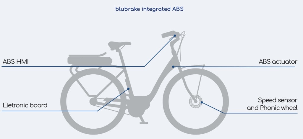
ABS for e-bikes
Blubrake wants your front wheel on an e-bike to have ABS, ensuring a safer cycling experience. The general trend in bikes is to replace rim brakes with disc brakes.
Blubrake min
Sun-powered E-trike
Wello has a hybrid pedal-powered trike that converts sunlight into electricity, giving you a boost.
Bicycle Computer
I’ve used CatEye, Garmin and Wahoo products for road cycling, and success draws competitors. This new computer from Million Concept Electronics is aimed at entry-level cyclists.
Million Concept Electronics – isport (Distance, speed, heart rate)
Bosch showed a new bike computer designed for e-bikes, it even controls a headlight and brake light, has a color display showing motor power versus pedal power, time of day, miles per hour, all sorts of analytics. There’s nothing from traditional bike computer makes like Wahoo, Garmin or CatEye designed specifically for e-bikes.
Kiox from Bosch, for e-bikes
Bio Sensors
Something totally new from Leomo is Type-S, a system with two sensors placed on your thighs and then a display with real-time analytics about how smooth your pedal stroke is, heel movement, even the pelvic angle, rock and rotation. Wow, there isn’t anything else like this in the world, although it’s something that would benefit a bike fitting session for sure.
Leomo min
Gaming Rollers
Real Design Tech has a set of rollers that you ride on, then use your bike to control a gaming joystick, pedals act like shooting controls.
I used my first rollers back in the 1970’s and the trick was how to balance without flying off the sides, because there were no guards to keep you in place. With the RealDesignTech rollers they’ve designed it so that you cannot fall off at all. To be viable they need to have a smart resistance unit and work with Zwift, instead of a proprietary system.
RealDesignTech
https://www.youtube.com/watch?v=lfNW3sqU4I4
Adaptive Suspension
Bumpy roads are the bane of cyclists, so HiRide has come up with electronically-controlled adaptive suspension for both Road and Mountain bikes.
HiRide adaptive suspension
Smart Lock
How about using your fingerprint to open a bike lock? That’s what BenjiLock showed, so no need to remember that key or combination again.
BenjiLock
Smart Glasses
Bosch will tout their Light Drive smart glasses that will help cyclists see more information from a bike computer system.
Light Drive from Bosch
Air-free Tires
I had 21 flats cycling in 2018, so yeah, I’m a bit interested in a flat-proof tire but it has to roll fast.
Bridgestone
Spin Bikes
In 2019 we watched the spin bike company Peleton go IPO and stumble in price, yet this category continues to grow with new entrants. The trainers come with a display and use WiFi to connect to an online instructor or workout sequence.
Myx FitnessEchelon EX 5S Indoor Cycle
You may be wondering what qualifies me to write about cycling, well for 2019 I biked 12,798.9 miles, so follow me on Strava, or let’s go for a ride when you visit Oregon. During the rainy winter months I do some virtual rides indoors on a Tacx Neo 2T smart trainer, using the Zwift app, so follow me: Daniel Payne (VV).
Just finished the 205 mile Seattle to Portland ride


