RVN! 26 Banner revised (800 x 100 px) (600 x 100 px)

Safety and Platform-Based Design

Safety and Platform-Based Design
by Bernard Murphy on 10-22-2019 at 5:00 am

Safety infrastructure in platform design

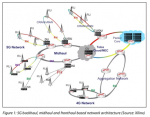
I was at Arm TechCon as usual this year and one of the first panels I covered was close to the kickoff, hosted by Andrew Hopkins (Dir System Technology at Arm), Kurt Shuler (VP marketing at Arteris IP) and Jens Benndorf (Managing Dir and COO at Dream Chip Technologies). The topic was implementing ISO 26262-compliant AI SoCs with Arm and Arteris IP, highly relevant since more and more of this class of SoC are appearing in cars. One thing that really stood out for me was the value of platform-based design in this area, something you might think would be old news for SoC design but which introduces some new considerations when safety becomes important.

A key aspect of platform-based design is being able to combine IP from multiple sources with differing levels of compliance to certain expectations, notably safety in this case. This can be most noticeable when you want to design part of the architecture to an ASIL D (safety critical) level while having enough safety diagnostic coverage to achieve ASIL B or C capabilities in other parts of the design. Designing an IP to this level entails a lot of overhead which may not be justified for safety-nominal (ASIL A/B) or even safety-indifferent (QM) components that you may want to use in your design.

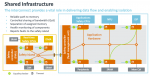
How then can you get your SoC to higher ASIL compliance? The answer lies in being able to ensure that safety-nominal systems cannot corrupt safety-critical functions and can be tested or taken offline if they malfunction. This is all significantly mediated by the network between the IPs, as indicated in the figure above. Among other functions this requires health monitoring for all components and of course reporting faults to a safety controller which can channel problems upstream to decision-making functions (are we in trouble, should the driver grab the wheel, pay special attention, pull the car over to the side of the road?).

Monitoring functions (all provided through or together with the interconnect) include time-out checks for data requests, IP isolation through powering down the appropriate NoC socket connection to run live LBIST checks (at suitable times), and finally end-to-end ECC error detection/correction.

This ability to monitor, check and isolate faulty IP provides the means to ensure ASIL B,C or D compliance at the system level, but depends also on a “cannot-fail” subsystem called a safety island. This is a special function designed fully to ASIL D requirements, with lockstep CPUs, independent memories and run-time testable cache and many more mechanisms to ensure independence from the rest of the system. This safety island continuously monitors for faults and will report (at presumably programed levels of concern) to higher-level decision-making functions in the car.

Closing the loop, Jens talked about a reference platform design they have built at Dream Chip using these capabilities and how that has been spun into several production derivatives. The reference design is based on a quadcore A53, an ISP and vision processor, peripherals and memory interfaces, all connected through an Arteris IP Resilient NoC, together with the safety island. They have a cool demo of this functioning in an autonomous car according to Kurt.

Derivatives modify this platform with different numbers of CPUs in the cluster and different IP subsystems for the vision processor (GPU, NPU or a simpler processor) for active mirror replacements, front-camera and radar applications. In a pre-safety platform, spinning these derivatives would be no big deal. For systems requiring a higher ASIL (B, C, or D), it is a big deal and what makes it possible is this safety modularity around functions, the ability to monitor, isolate and ECC check through the interconnect and a carefully isolated safety island. All of these guarantee higher ASIL operation no matter what else in the SoC may go wrong.

You can learn more about this design by downloading the Arm TechCon presentation HERE.


GLOBALFOUNDRIES and Arm Showcase Broad Range of Partnership

GLOBALFOUNDRIES and Arm Showcase Broad Range of Partnership
by Randy Smith on 10-21-2019 at 10:00 am

I previously blogged on the GLOBALFOUNDRIES (GF) Technology Conference (GTC) held in Santa Clara, CA. The main takeaway that I shared in that blog was that GF’s announced “pivot” to a specialty foundry announced over a year ago, including its decision not to pursue 7nm and smaller nodes, appears to be working and GF is gaining momentum. There was not enough room in that blog to go into what I feel is another strategic decision GF made that is serving this transition well – its deep and broad relationship with Arm®. As many activities are going on between these companies, let me first break this into two broad categories – foundation IP and computing IP.

To have a thriving ecosystem on any given manufacturing process requires a strong collection of base-level IP, including standard cells, IO cells, memory compilers, and other basic building blocks. Collectively, I refer to this as foundation IP. Other IP providers and GF customers build their IP on top of the foundation IP. In my opinion, and I am admittedly biased1, TSMC’s rapid rise from $387M quarterly revenue in Q1 1998 to $2.5B by Q2 2006, coincided with its decision to have much of its foundation IP supplied by Artisan Components starting with TSMC’s 0.25-micron process in March of 1998. Arm announced its acquisition of Artisan® in August 2004. The foundry model took off in part due to the availability of foundation IP that was as good or better than what semiconductor manufacturers were developing themselves.

As a specialty manufacturer, GF has a large collection of processes. GF needs to make sure each process has a solid IP foundation. More than that, since each process is intended for a different field of use, that foundation IP should be tailored for the specific needs of designers using that process (e.g., low power design for a low power process, etc.) – a generic library is not very helpful. Along those lines, last month GF announced its 12LP+ solution, which makes use of Arm Artisan physical IP and ARM POP  IP (more on POP IP later in this blog). These libraries are available now, and tape-outs are expected in 2020.

Arm Comprehensive Physical IP Platform at GF 12LP

  • Two logic library architectures (SC7.5, 9)
  • Nine memory compilers
  • GPIO for 1.8V and 3.3V
  • Specially optimized single rail 0.55V low-voltage compilers
  • Single-Fin Logic libraries to enable lowest power designs

Just two months ago, GF and Arm announced that they had taped out “an Arm-based 3D high-density test chip that will enable a new level of system performance and power efficiency for computing applications such as AI/ML and high-end consumer mobile and wireless solutions.” This unique project made use of breakthrough technology from both companies to come up with a more advanced packaging solution that should benefit GF customers needing a lower latency, higher bandwidth solution for applications such as AI and ML.

Gus Yeung

At GTC, there was a joint presentation by Ted Letavic, GF VP and Senior Fellow and Gus Yeung, GM VP and Fellow, Physical Design Group, Arm. Ted spoke about many innovations GF is developing under its specialty strategy, including IP coming from many other IP suppliers. There was again the GF Innovation Equation, which was prominent throughout the event and featured IP as a multiplier in supplying innovation to GF customers. Gus focused a bit more on ML,

Ted Letavic

showing the path Arm and GF are taking together in this rapidly evolving market. The partnership also includes Arm’s POP IP, which is a core-hardening acceleration technology. POP gives you Arm’s expertise captured in a way to accelerate your implementation of specific Arm cores while minimizing area, leakage, and dynamic power while also optimizing performance.

There is so much going on between GF and Arm, that I am sure to have left some things out. This relationship is certain to benefit both companies, and I am looking to further progress they can achieve together.

1 Randy Smith previously served as Artisan Components Director, Japan Sales, and Vice President of Corporate Ventures.


WEBINAR: PAVE360 Validating Autonomous Vehicle Behavior

WEBINAR: PAVE360 Validating Autonomous Vehicle Behavior
by Daniel Nenni on 10-21-2019 at 6:00 am

Siemens Mentor recently announced PAVE360™, a very cool comprehensive pre silicon simulation environment. Autonomous cars are very popular here in Silicon Valley and quite safe on the highways since the average speed is 25mph (horrible traffic). In the city you need autonomous parking unless you want to waste precious time scavenging for a spot and climbing out your window since spaces continue to shrink and cars continue to grow. Kind of like airline seats.

The problem is that the lines of software code that power these new vehicles is increasing exponentially and validating the silicon and software integration is incredibly time consuming. I was very fortunate to work for one of the brilliant minds behind silicon simulation and I am honored to quote him here:

“PAVE360 represents the first output of an innovation process born from the combination of Mentor and Siemens employees, ideas, and technologies two years ago,“ said Ravi Subramanian, vice president and general manager of the IC Verification Solutions Division of Mentor, a Siemens business. “PAVE360 from Siemens delivers a comprehensive program to support the deep, cross-ecosystem collaboration necessary for our customers to develop powerful custom silicon and software solutions to power the autonomous vehicles revolution.“

To dig into PAVE360 further I organized a webinar with Mentor. I hope to see you there:

WEBINAR: PAVE360 Validating Autonomous Vehicle Behavior

Abstract: Validating an SoC for intelligent vehicles requires much more than conventional methodologies have used. In fact, correctness is only defined in the context of the physical environment, vehicle dynamics and occupant survivability. Mentor/Siemens’ PAVE360 addresses this complexity with a holistic engineering methodology pioneered by the smartphone industry and refined to apply to intelligent vehicles.

Presented by David Fritz: With over 25 years of experience in the Semiconductor industry having held senior technical roles at NVidia, Qualcomm, Texas Instruments, and others, Mr. Fritz leads the global autonomous IC and validation initiative at Siemens Mentor. Mr. Fritz brings innovation and entrepreneurial drive of fast moving Silicon Valley companies to the Siemens Mentor team by applying transformative technologies to the challenges of autonomous and connected vehicles.

About PAVE360
Democratizing Automotive IC Design and Development
As advances in processing continue to play an increasingly prominent role in automotive evolution, carmakers are turning to custom silicon designs to deliver the “just right” blends of cost, power, performance and advanced features necessary to enable an autonomous future.

With PAVE360, chip design can be democratized, enabling carmakers, chipmakers, tier one suppliers, software houses and other vendors to collaborate on the development and customization of extraordinarily complex silicon devices for autonomous vehicles. PAVE360 delivers a robust platform for this collaboration, helping to speed chip design and software validation, and enabling the creation of model-specific silicon for the first-generation of self-driving cars.

PAVE360 establishes a design-simulation-emulation solution that scales from individual blocks of a system-on-chip’s (SoC’s) IP, to hardware and software on the SoCs, to vehicle subsystems, and up through deployment of vehicles in smart cities – a true “chip-to-city” approach based on the increasing digitalization of the automotive industry.


ASML – In Line Qtr but big bookings – Logic Strong! Memory ? EUV?

ASML – In Line Qtr but big bookings – Logic Strong! Memory ? EUV?
by Robert Maire on 10-20-2019 at 6:00 am

ASML in line QTR with big Orders
Near term slippage w long term upside
Logic is strong but memory recovery unknown
EUV is finally a reality/commercialized

In line quarter- supplier slippage expected in Q4
Results were revenues of Euro 3B and EPS of Euro 1.49, more or less in line with earnings estimate if a tad bit light in revenue. Outlook for Q4 is Euro 4B with 4 EUV systems slipping into 2020 due to supplier issues (now resolved)

Logic is leading the recovery… Obviously TSMC
Over 70% of orders are from foundry/logic customers as everyone is getting in the queue now that EUV is in commercial production. TSMC is the leader in real EUV and likely accounts for the largest portion of those future EUV orders

Memory still an unknown
Several months ago we said that the recovery would be led by logic as the memory recovery would take longer than most people expected due to the sidelined capacity amid excess supply and weak pricing.

This is becoming clearer to most people as we have heard from Micron, which was weaker than many expected and now clearly hearing from ASML that memory business remains weak with unknown timing of a recovery.
Some are expecting a recovery early in 2020, but we would not get our hopes up as it could take all of 2020 to get memory back on track.

Huge orders Euro 5B and 23 EUV tools
ASML is selling out its capacity very quickly as we are now seeing a virtual avalanche of orders. EUV has been proven and no customer wants to be excluded from the party or perhaps run out of capacity.

Part of the huge ramp is the large ramp in the numbers of layers in a chip made with EUV, going from a few ,like 3-5, going to 12 to 15 (depending upon whom you believe). Basically the number of tools has to increase proportionately with the number of layers. Memory is still a long way away from using EUV so in our view the current memory weakness, while impacting DUV and immersion is not slowing down EUV.

In a perverse way, the weakness in EUV demand for memory is likely of benefit to the logic side of the industry as it doesn’t compete for limited EUV tool availability.

40 plus EUV tools should be very easy to book for next year as we are more than halfway there. I think we can get there even without any memory recovery.

Not worried about supplier slippage
Given the complexity of an EUV tool and the huge supply chain we are certainly going to see issues here and there. The fact that its only a one quarter slip suggests its not a big or systemic problem.

We would likely take a longer term view as to the overall trend and worry less about the actual ship date and whether it falls within one quarter or another. ASML is not in a “turns” business like dep and etch or other relatively simple to assemble tools.

It down to production execution
As we are now past the milestone of actual commercial EUV production we are past the point of invention, luck, and pain and suffering trying to get the technology to work and more focused on production issues and the ramp of manufacturing.

To be sure, there are still many issues out there, pellicles, resist, reticle inspection, but what we have is working well enough to push forward on the number of layers using EUV and thus more tools.

We have covered ASML for almost 25 years with much of that history watching the EUV saga play out, so it is interesting to see the final conclusion (or perhaps beginning) of an era.

The stock –
Priced for perfection in an imperfect world, but still pretty good. ASML’s stock has steadily climbing based on the view of a recovering chip sector. Some stocks in the space have gotten a bit ahead of themselves but we think ASML’s value increase is justified given where we are with EUV, the strong logic/foundry demand and overall positioning in the market. Some investors may be unhappy with the slippage, but we are less concerned as you have to look at the longer term.

Some investors may be unhappy with a quarter that was just “in line” but given the memory weakness, we think “in line” is very good performance as ASML is working with one hand (memory) tied behind its back.

Overall we remain constructive on the stock and would look at pull backs or weakness as an opportunity to build or enhance a position going forward.
The stock is not cheap but the performance and positioning support the valuation.

We think that ASML has the lowest China/US trade problem exposure (though not zero) and EUV sales are less impacted by near term economic gyrations as the backlog is likely very strong. All in all a relatively defensive position in a very cyclical industry.

Summary
ASML remains a virtual monopoly, with a huge defensive moat, upside potential in revenues and margins and a leading technology position. We expect margins and therefore profitability to increase steadily as EUV ramps over the next few years leading to long term upside. It remains one of our top picks in large caps in the space.


TSMC – Solid Q3 Beat Guide- 5G Driver – Big Capex Bump – Flawless Execution

TSMC – Solid Q3 Beat Guide- 5G Driver – Big Capex Bump – Flawless Execution
by Robert Maire on 10-19-2019 at 6:00 am

TSMC puts up solid QTR, Capex increase for 5NM and capacity increase, 5G/mobile remains driver- HPC good 7NM, 27% of revs- Very nice margins!

In line quarter-Good guide
TSMC reported revenues of $9.4B and EPS of $0.62 , more or less in line with expectations, perhaps a touch below ” whisper” expectations which had been growing along with the lead times for 7NM. Gross margin was a nice 47.6%.
Q4 is expected to be between $10.2B and $10.3B with gross margins between 48% and 50%. This revenue outlook is well above current street expectations.

Large bump up in Capex
We have been talking about a logic led recovery, in chip equipment, given the strength at TSMC. TSMC bumped up their 2019 capex from $12.5B to $14 to $15B with initial outlook for 2020 to be similar to 2019.

This suggests a bit of a hockey stick like capex spend in the current Q4 of 2019.This hockey stick will show up in a better than expected guide from tool companies

We think this is likely a strong mix of not only 5NM spend but also 7NM capacity related spend given better than expected demand and long lead times currently seen by customers.

Capex intensity, currently at 40% is expected to come down in 2020 and further come down in 2021 to 30% to 35%

5G and mobile remains the big upside in demand
In our view, customers in the mobile space are all rushing to get to market first with 5G devices to try to stake a claim to market share and early dominance. This has created a strong “land rush” of orders to insure enough 5G chips to power those devices.

7NM was 27% of total sales which supports this strong demand and suggests strong pricing ability as well.

This is quite a strong ramp from the start of 7NM earlier in the year. We are sure that HPC (read that as AMD) is also clearly helping to drive demand over the top.

Smartphone was 49% of revenue with HPC at 29%.

We don’t think any significant portion of sales was due to inventory build or channel stuffing as fears of trade ware related cut offs have subsided in the market.

TSMC winning on both yield and packaging
In our view, we think that TSMC is attracting more customers and thus the longer lead times as they have both better yields and better packaging technology.

We think Samsung has had more struggles with yield and coming up to speed despite (and potentially because of ) EUV implementation.

We also think that TSMC’s advanced capabilities in packaging allow it to offer customers more and better options in 2.5 and 3D packaging.

As customers look for other strategies outside of Moore’s law scaling, such as “chiplets”, these packaging options become a critical differentiating and enabling technology. Some customers, such as AMD, are currently banking on advantages of a “chiplet” architecture.

Collateral impact on equipment companies
TSMC’s report , and large capex increase, confirms our view that there is a strong near term pick up in equipment demand despite memory “sucking wind”.

We think most equipment suppliers will report at least in line or likely better than expected results in the current quarter but more importantly will guide even higher going forward as orders from TSMC hit their order books.

This is very much in line with our “logic/foundry led recovery” that we have talked about for several months. While not a rip roaring semicap recovery, its better than the bouncing along the bottom that the industry has been stuck with and importantly puts an upward bias on business even though the slope may be low without memory.

The Stock – Nice quarter, but perhaps not up to the unrealistic expectations of the market
Its clear that chip stocks have been on a tear and along with the stocks, and so have expectations. Much of this in TSMC’s case is a combination of Apple talking about increasing supplier orders by 10% along with the extended lead times at TSMC 7NM. We think expectations and the stock both got a little bit ahead of themselves such that when the company reported an excellent quarter, such as it did, that investors were unimpressed as it didn’t blow away numbers.

We would use any weakness as an entry point to add to positions in TSMC.

They are now more dominant in foundry than ever before and if anything they are lengthening their lead over number two Samsung. Near term demand looks very good, margins are good and getting better.

Most importantly, TSMC continues to push Moore’s Law forward without any visible hiccups or delays…..perhaps they make it look too easy…..perhaps they should have a one quarter “oops” to make them look human and reset investors expectation of perfect performance in technology execution.

They have a very long runway of upside in 5G , with little competition, ahead of them. They are also the “real” engine behind AMD’s success and will get their fair share of the upside associated with that and other HPC business.

We like companies that have dominant or monopolistic-like positions, great execution on technology with a strong defensive “moat” . All this usually combines to show up in financial performance and future upside which we clearly have with TSMC.

We continue to be a buyer of the stock and would be more aggressive on pullbacks. Our only significant cautions would be trade and macro economic risk that all chip companies share.


The New Silvaco CEO is SURGING!

The New Silvaco CEO is SURGING!
by Daniel Nenni on 10-18-2019 at 6:00 am

One of my great pleasures in the semiconductor industry is meeting the people who have brought us to where we are today, at the forefront of modern life. One of those people is Babak Taheri, now CEO of Silvaco who I spent time with yesterday. Babak started in semiconductors around the same time I did 30+ years ago. He has a PhD in EECS and Neurosciences from UC Davis, a Masters Degree from San Jose State and his Bachelors from San Francisco State so he is truly a Silicon Valley native. He held executive positions in engineering, R&D, and corporate management at leading technology firms including Freescale, Cypress Semiconductor, Apple, Invensense, and SRI International, he is also the holder of 28 patents.

Babak came to Silvaco as the CTO last year and was bumped up to CEO in August when David Dutton decided to go back to the equipment manufacturing business. David however is still involved with Silvaco as the Vice Chairman of the board. Having known Silvaco since its beginning I am VERY impressed by this move.

Next week is the Silicon Valley Silvaco SURGE event where Babak will be giving the keynote : From Atoms to Systems. As we all know the semiconductor business is very systems orientated now so it will be interesting to see Babak’s perspective, absolutely.

SURGE brings the TCAD, EDA, and IP communities together to discuss new technologies, explore smart application integration, and discover innovative techniques for advanced semiconductor design. The event includes eight demo stations, a catered lunch, and cool prizes and giveaways for attendees.

  • Executive keynotes
  • Technology Tracks: TCAD, EDA and Design IP
  • Roadmap presentations
  • Customer and partner presentations and success stories
  • Eight unique demo stations
  • Networking with industry experts

SURGE is at the Santa Clara Marriott again this year so you can bet that the food will be great. Take a look at the agenda, after the keynotes there are EDA, TCAD, and IP tracks so something for everyone. As much as I love EDA, I’m all about IP these days so that is where I will be.

I hope to see you there!

About Silvaco
Silvaco Inc. is a leading EDA tools and semiconductor IP provider used for process and device development for advanced semiconductors, power IC, display and memory design. For over 30 years, Silvaco has enabled its customers to develop next generation semiconductor products in the shortest time with reduced cost. We are a technology company outpacing the EDA industry by delivering innovative smart silicon solutions to meet the world’s ever-growing demand for mobile intelligent computing. The company is headquartered in Santa Clara, California and has a global presence with offices located in North America, Europe, Japan and Asia. For more information, visit Silvaco.com.


The SiFive Tech Symposiums are Heading To Portland and Seattle Next Week!

The SiFive Tech Symposiums are Heading To Portland and Seattle Next Week!
by Swamy Irrinki on 10-17-2019 at 2:00 pm

We’re confirming seats in Portland and Seattle for the Pacific Northwest leg of our worldwide 2019 SiFive Tech Symposiums. We are pleased to have Mentor, A Siemens Business as our co-host, and Lauterbach, a leader in microprocessor development tools, as our partner in both cities. The Portland symposium will take place Tuesday, October 22 at the Portland Community College. Our Seattle symposium will be on Wednesday, October 23 at thinkspace Seattle. All of the SiFive Tech Symposiums have been significantly instrumental in engaging the hardware community in the RISC-V ecosystem, and spearheading the emergence of new applications. We are constantly in awe of the brilliant minds that convene at these events. We thrive on watching intense conversations and the sharing of ideas between those already entrenched in RISC-V and others who are simply exploring design alternatives.

The symposiums in Portland and Seattle will both feature presentations by the RISC-V Foundation, SiFive, Mentor and Lauterbach, as well as other ecosystem partners and academic luminaries. There will also be a tutorials, demos and presentations on RISC-V developments tools, platforms, core IP and SoC IP. As always, we have arranged for plenty of time for networking.

Attendance is free, but registration is required!

  • To view the agenda, and to confirm your seat in Portland, please click here.
  • To view the agenda, and to confirm your seat in Seattle, please click here.

We look forward to seeing you!

About SiFive
SiFive is the leading provider of market-ready processor core IP, development tools and silicon solutions based on the free and open RISC-V instruction set architecture. Led by a team of seasoned silicon executives and the RISC-V inventors, SiFive helps SoC designers reduce time-to-market and realize cost savings with customized, open-architecture processor cores, and democratizes access to optimized silicon by enabling system designers in all market verticals to build customized RISC-V based semiconductors. With 14 offices worldwide, SiFive has backing from Sutter Hill Ventures, Spark Capital, Osage University Partners, Chengwei, Huami, SK Hynix, Intel Capital, and Western Digital. For more information, www.sifive.com.

About the RISC-V Foundation
RISC-V (pronounced “risk-five”) is a free and open ISA enabling a new era of processor innovation through open standard collaboration. Founded in 2015, the RISC-V Foundation comprises more than 325 members building the first open, collaborative community of software and hardware innovators powering innovation at the edge forward. Born in academia and research, the RISC-V ISA delivers a new level of free, extensible software and hardware freedom on architecture, paving the way for the next 50 years of computing design and innovation.

The RISC-V Foundation, a non-profit corporation controlled by its members, directs the future development and drives the adoption of the RISC-V ISA. Members of the RISC-V Foundation have access to and participate in the development of the RISC-V ISA specifications and related HW / SW ecosystem. The Foundation has a Board of Directors comprising seven representatives from Bluespec, Inc.; Google; Microsemi; NVIDIA; NXP; University of California, Berkeley; and Western Digital.

In November 2018, the RISC-V Foundation announced a joint collaboration with the Linux Foundation. As part of this collaboration, the Linux Foundation will also provide an influx of resources for the RISC-V ecosystem, such as training programs, infrastructure tools, as well as community outreach, marketing and legal expertise.

Each year, the RISC-V Foundation hosts global events to bring the expansive ecosystem together to discuss current and prospective RISC-V projects and implementations, as well as collectively drive the future evolution of the instruction set architecture (ISA) forward. Event sessions feature leading technology companies and research institutions discussing the RISC-V architecture, commercial and open-source implementations, software and silicon, vectors and security, applications and accelerators, simulation infrastructure and much more. Learn more by visiting the Event Proceedings page.


eSilicon White Paper on Chiplets – Good Read

eSilicon White Paper on Chiplets – Good Read
by Randy Smith on 10-17-2019 at 10:00 am

eSilicon recently released a paper detailing its experiences and its thoughts on the future of chiplets. The author of the white paper is Dr. Carlos Macián. I have also covered a presentation given by Carlos recently at the AI Hardware Summit, and he is well-spoken and quite knowledgeable. To get the white paper, go to the eSilicon website white paper page where you can access a lot of white papers they have developed.

Chiplets are more than an interesting concept. There are many large companies and start-ups all investing in this approach. Even the US government, in the form of the Defense Advanced Research Projects Agency (DARPA), is trying to develop a useful methodology for this approach. So, what is a chiplet?

When you design using chiplets, you put multiple dies into the same package. This approach by itself is not a new technique. We have had multichip modules (MCM) for quite some time. But, MCM designs were usually reserved for high-end, somewhat expensive products. Today’s chiplet market is not about stacking a big memory die over a big processor die. The modern chiplet market is about standardizing the connection method to place multiple dies on a substrate to build a complete system. The problem is, there is not a standard specification for chiplets.

One of the benefits of using a chiplet approach is that you can develop each chiplet in a different technology node, and of course they can be from different manufacturers. This method would seem to be a more efficient approach than putting everything in one very fast expensive process, if not all of the design implementation needs to be at that expensive node. Analog or RF portions of the design may very well be best suited to 28nm or higher. Slower portions of the design may be just fine at 90nm. But, these chiplets have to “plug in” to the substrate used to connect them. To make an effective market out of this, you need a standardized “socket.”

The appropriate socket will depend on the target market. There are low-end applications that could plug in multiple sensors, small processors, small radios, and a bit of memory to make IoT devices. These could be done using a BGA model, though the pitch and electrical interfaces would need some standardization. There are already companies trying to build a design environment around this approach, such as zGlue. You could use faster chip-to-chip interfaces such as those from NVIDIA, Intel, or eSilicon for higher-end applications with 2.5D/3D interconnects, and other approaches to get memory closer to the processors, creating a huge benefit. This approach to chiplets is a good method for some designs, but if you want to be a chiplet provider, how do you standardize your chiplet products across the different vendor technologies? Then there is DARPA, who might be able to build a solution that is not as dependent on what is best from a cost perspective. You can read more about DARPA’s Common Heterogeneous Integration and IP Reuse Strategies (CHIPS) program here.

I think Carlos’ white paper provides the answer applicable to the sweet spot of this market. I don’t expect an off-the-shelf market to develop anytime soon for high-end applications. But data center, machine learning, domain-specific processors, and other high-performance, high-efficiency solutions are needed right now. Fortunately, this technology is also available now. Grab the eSilicon white paper here.


Virtualizing 5G Infrastructure Verification

Virtualizing 5G Infrastructure Verification
by Bernard Murphy on 10-17-2019 at 5:00 am

5G backhaul, midhaul, fronthaul

Mentor have pushed the advantages of virtualized verification in a number of domains, initially in verifying advanced networking devices supporting multiple protocols and software-defined networking (SDN), and more recently for SSD controllers, particularly in large storage systems for data centers. There are two important components to this testing, the first being that simulation is clearly impractical; testing has to run on emulators simply because designs and test volumes are so large. The second factor is that the range of potential testing loads in these cases is far too varied to consider connecting the emulator test platform to real hardware, the common ICE model for testing in such cases. The “test jig” to represent this very wide range must be virtualized for pre-silicon (and maybe even some post-silicon) validation.

Jean-Marie Brunet, Dir. Marketing for Emulation at Mentor, has now released another white paper following this theme for 5G, particularly the radio network infrastructure underlying this technology. This makes for a good yet quick read for anyone new to the domain, in part on what makes this technology so complex. In fact “complex” hardly seems to do justice to this standard. Where in simpler times we’ve become familiar with mobile/edge devices connecting to base stations and from there to the internet/cloud through backhaul, in 5G there are more layers in the radio access network (RAN).

These are not only for managing aggregation and distribution. Now backhaul to the internet connects (typically through fiber) to the central unit (CU) which handles baseband processing. The CU then connects to distribution units (DUs) and those connect to remote radio units (RRUs), which are possibly small cells. The CU to DU connection is known as midhaul and the DU to RRU connection is known as fronthaul. (More layers are also possible.) This added complexity has been designed to allow for greater capacity with appropriate latency in the fronthaul network, for example ultra-low latencies are only possible if traffic can flow locally without need to go through the head node.

With this level of layering in the network it shouldn’t be surprising that operators want software-defined networking, in this domain applied to something called network slicing to offer different tiers of service. It also shouldn’t be surprising to learn that more compute functionality is moving into these nodes, known here as Multi-Access Edge Computing (MEC), more colloquially as fog computing. If you don’t want to take the latency hit of going back to the cloud for everything, you need this local compute. And I’m guessing the operators like it because this can be another chargeable service.

Then there’s the complexity of radio communication in ultra-high-density edge-node environments. This requires support for massive MIMO (multi-input-multi-output) where DUs and possibly the edge nodes themselves sport multiple antennae. The point of this is to allow communication to adaptively optimize, through beamforming, to highest available quality of link. Some indications point to that link adaptation moving under machine-learning (ML) control since look-up table approaches in LTE are becoming too complex to support in 5G.

ML/AI will also play a role in adaptive network slicing, judging by publications from a number of equipment makers (Ericsson, Nokia, Huawei et al). This obviously has to be robust around point failures in the RAN, and it also needs to be able to adapt to ensure continued quality of service in guaranteed latency provisions. I also don’t doubt that if ML capability is needed anyway in these RAN nodes, operators will be tempted to add access to that ML as an additional service to users (perhaps for more extensive natural language processing for example).

So – multi-tiered RANs, software-defined virtual networks through these RANs, local compute within the network, massive MIMO with beamforming and intelligently adapted link quality, machine learning for this and other applications – that’s a lot of functionality to validate in highly complex networks in which many equipment providers and operators must play.

To ensure this doesn’t all turn into a big mess, operators already require that equipment be proven out in compliance-testing labs to be allowed to sit within and connect to sub-5G networks. This concept no doubt continues for 5G, now with all of these new requirements added. Unit validation against artificially constructed tests and hardware rigs is a necessary but far from sufficient requirement to ensure a reasonably likelihood of success in that testing. I don’t see how else you could get there without virtualized network testing against models running on an emulator.

You can read the Mentor white-paper HERE.


Optimizing High Performance Packages calls for Multidisciplinary 3D Modeling

Optimizing High Performance Packages calls for Multidisciplinary 3D Modeling
by Tom Simon on 10-16-2019 at 10:00 am

For all the time we spend thinking and talking about silicon design, it’s easy to forget just how important package design is. Semiconductor packages have evolved over the years from very basic containers for ICs into very specialized and highly engineered elements of finished electronic systems. They play an important role in every aspect of chip operation. New packaging technologies, such as 3D IC, SiP, etc., have actually made packages integrated to chip operation. Package design and analysis is becoming more critical because packages can strongly influence cost, reliability, performance, area and a host of other characteristics.

The list of “care abouts” for package design has become pretty long and without a doubt calls for a multidisciplinary approach. Packages essentially are the cocoon that protects the IC die from the effects of its environment. Outside the package there can be threats from moisture and physical shock and vibration. The package also plays a critical role in removing thermal energy away from the IC. Due to expansion and contraction of materials with different CTEs, thermal stress arises at material interfaces in the package. Ultimately, this stress can cause fractures and cracking, leading to failures. Packages also play a significant role in signal and power integrity, which is extremely important for high speed RF and digital applications.

Because of the wide range of factors and issues involved in package design, a comprehensive approach is called for. Dassault Systèmes offers an in-depth solution for every aspect of package design. The3DEXPERIENCE platform allows designers to look at electromagnetic, thermal, and mechanical design considerations using advanced 3D simulators and solvers. With Knowledge Based Modeling, design changes can be quickly updated and analyzed. 3DEXPERIENCE offers the tools and infrastructure to enable rapid design updates to all stakeholders to accelerate the design process.

The solvers in the CST Studio Suite can be used for a wide range of electromagnetic, thermal and mechanical simulations. Applying them to package design and analysis allows designers fully understand each of the multi-disciplinary aspects of the package design. The integrated environment allows a DOE approach to specifying and verifying the package design to fully understand the performance tradeoffs.

Dassault Systèmes has also thought a lot about the user experience for engineers using the 3DEXPERIENCE platform. They offer advanced HPC capabilities and Cloud computing services for faster throughput and reduced simulation costs. Dassault Systèmes has built lightweight visualization technologies for viewing and sharing 3D models and simulation results in web-based apps.

Packaging can be make-or-break for many semiconductor products and systems. This is especially true when looking at product lifecycle management and reliability. It is one thing to design something that works when brand new, but over time residual stresses from operation and the environmental impact can lead to reduced fatigue life or even failure. In applications such as automotive, the expected lifetime of a product in the field should extend out decades, way beyond the expected lifetime of many consumer gadgets. The economic or even human cost of a failure can also be incredibly high.

The Dassault Systèmes website has detailed information on their solutions for advanced electronics packaging. For more information click HERE.

Also Read

A Brief History of IP Management

Delivering Innovation for Regulated Markets

Webinar: Next Generation Design Data & Release Management