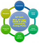
Bronco Webinar 800x100 1

Debugging Hardware Designs Using Software Capabilities

Debugging Hardware Designs Using Software Capabilities
by Daniel Nenni on 12-20-2019 at 6:00 am

Every few months, I touch base with Cristian Amitroaie, CEO of AMIQ EDA, to learn more about how AMIQ is helping hardware design and verification engineers be more productive. Quite often, his answers surprise me. When he started describing their Design and Verification Tools (DVT) Eclipse Integrated Development Environment (IDE), my first reaction was that engineers had plenty of GUIs at their fingertips already. When he talked about Verissimo SystemVerilog Testbench Linter, I said that lint surely must be a solved problem by now. Then I wondered how the Specador Documentation Generator differs from all the shareware solutions available. In my most recent talk with him, the topic was AMIQ EDA’s DVT Debugger, their fourth major product. Given that simulators have built-in debuggers I was curious once again how their tools are differentiated and how they actually make money.

As in our previous discussions, Cristian was clear in describing the limitations of other solutions, including features built into other tools. In the case of interactive debugging of test cases, the major simulators do have some nice capabilities. However, the GUIs are different and proprietary, so moving from an IDE to a simulator for debug is jarring. If the project uses multiple simulators, a not uncommon practice, the engineers are cycling through multiple screens constantly. The DVT Debugger is an add-on to the DVT Eclipse IDE, so users can debug in the same environment that they use to write, analyze, and visualize their design and verification code in SystemVerilog, VHDL, or the e language. The tool supports all major simulators, so even with multiple vendors involved the debug interface is unchanged.

The DVT Debugger provides all the interactive functionality that software programmers enjoy, applied to design and verification code. The debugger can launch a new simulation run or connect to an existing run on the same machine or on the network. Users can insert breakpoints into their code, including conditional breakpoints, and enable or disable them. A breakpoint stops a running simulation to allow examining the values of variables to see what is happening in the design and testbench. It is possible to change variable values before resuming the run or starting a new one. Under user control, the debugger can step line by line through the code, step over (skip) a line of code, or step into or out of a function. The complete call stack is displayed, and users can move up or down. Users can define and watch complex expressions for more insight into the running code. Further, dedicated views display the simulation output and allow typing commands directly to the simulator.

While using all these debugging features, users remain within the IDE. They can take advantage of all the navigation and visualization features for which the DVT Eclipse IDE is known. These include tracing signals, finding usages, generating schematic views, and cross-probing across the wide range of available views. The Debug View and the code editor are always synchronized. For example, when the user moves up and down the call stack, the active line corresponding to the selected stack frame is automatically highlighted. Similarly, the Variables View displays the variables associated with the stack frame selected in the Debug View. These include the arguments of the current function, locally declared variables, class members, and module signals. Users can change variable values at runtime from this view.

A powerful debugger is required for modern hardware designs. Cristian reminded me of the old-fashioned way of debug: adding print statements to the code to trace what’s happening. Well-designed debug messaging is valuable, but iteratively adding temporary statements is tedious and error-prone since engineers must guess the source of a test failure and re-compile every time they change the code. These temporary print statements should be deleted so they do not reduce code readability and clutter simulation output once the bug is fixed, but editing code excessively introduces more risk. Controlling a simulation as a test runs, having full visibility into all variables, and modifying variables to exercise “what-if” scenarios make for a more scalable and more efficient process.

I asked Cristian whether DVT Debugger users ever use the debuggers built into the simulators, and he said that they do. Simulation vendors provide a lot of “hooks” for other tools to link in but there may be features available only in their own debuggers that require proprietary connections. He said that the goal of their tool is not to replace simulator debuggers but rather to offer a rich, software-like debug experience in the same environment where design and verification engineers write their code. As in their other products, AMIQ EDA has taken powerful, proven techniques originally developed for programmers and adapted them to add value to the hardware design and verification flow. As Martha Stewart used to say, it’s a good thing.

To learn more, visit https://www.dvteclipse.com/products/dvt-debugger.

Also Read

Automatic Documentation Generation for RTL Design and Verification

An Important Next Step for Portable Stimulus Adoption

With Great Power Comes Great Visuality


Network on Chip Brings Big Benefits to FPGAs

Network on Chip Brings Big Benefits to FPGAs
by Tom Simon on 12-19-2019 at 10:00 am

NAPs provide connection to high speed NoC

The conventional thinking about programmable solutions such as FPGAs is that you have to be willing to make a lot of trade-offs for their flexibility. This has certainly been the case in many instances. Even just getting data across the chip can eat up valuable routing resources and add a lot of overhead. These problems are exacerbated when wide or fast transfers are needed. In ASIC based SoCs it is easy to add IP for high speed interfaces. However, in FPGAs valuable logic units are often used to implement these same interfaces. It turns out that using one type of solution that is used in ASICs for connecting blocks is also a big win for FPGAs. We see Network on Chip (Noc) used a lot for ASICs, and now they have found a home in FPGA’s. The number of benefits they provide may surprise you.

Achronix has written an interesting white paper that covers eight benefits that come from the addition of a NoC in their Speedster7t FPGA. Their NoC is specialized to address the needs of an FPGA. It is arranged in vertical and horizontal channels that travel through the FPGA core. Each channel has two uni-directional high speed buses that operate at 512 Gbps. The FPGA also retains its traditional FPGA routing structure. NoC Access Points (NAP) located at the row and column intersections are used to make connections to the NoC. The NoC connects to all external interfaces for memory and networking.

I won’t go through each of the eight benefits here, but I want to discuss a few of them.

Two of the benefits have to do with the ability to connect to PCIe and 400G Ethernet. Making a PCIe interface work in an FPGA requires detailed work to understand placement and routing to manage delays and throughput. With a NoC, much of the work that previously required time and FPGA resources is handled automatically. Not only is design time saved, but also testing and debugging is reduced.

400G Ethernet also gets a boost from the NoC. Using their new Packet Mode, incoming packets are cascaded across four independent 256 bit buses in parallel, so that packets are efficiently conveyed. Packets are interleaved across these four buses so the FPGA can efficiently keep up with the incoming data stream.

One of the surprising benefits relates to how multiple teams can work more efficiently on FPGA projects that contain a NoC. Traditionally team design has been difficult to perform because of conflicts in accessing interconnect resources in the FPGA fabric. With the Achronix Speedster7t NoC any design block in the FPGA can access any other through the NAPs connected to the NoC. This suddenly removes any issues with placement or interconnect resources from the design design considerations.

The Achronix white paper has several other surprising benefits relating to how their NoC improves the design process. The NoC together with their high performing FPGA fabric is a winning combination. This is especially true for machine learning applications because of the specially architected Machine Learning Processors (MLP) found in the Speedster7t. I suggest reading the white paper, entitled “Eight Benefits of Using an FPGA with an On-chip High-Speed Network”. It is available for download on the Achronix website.


Full Solution for eMRAM Coming in 2020

Full Solution for eMRAM Coming in 2020
by Tom Simon on 12-19-2019 at 6:00 am

Trimming for eMRAM in Tessent

It’s amazing to think that Apollo moon mission used computers that were based on magnetic core memories. Of course, CMOS memories superseded them rapidly. However, over the decades since, memory technologies have advanced significantly, in terms of density, power and new types of technologies, e.g NAND Flash. Ever since the 90’s magnetoresistive technology has been under investigation. Now Spin Torque Transfer Magnetic Random Access Memory (STT-MRAM) is becoming feasible and bringing with it many advantages over SRAM and/or NAND Flash. STT-MRAM fits in an interesting niche where it can be used for a variety of applications with big benefits.

In particular, it is very well suited for embedded memory applications. Embedded MRAM (eMRAM) has a much smaller cell size than SRAM, being comparable to NAND Flash. However, unlike NAND Flash it only requires an additional 2 or 3 mask layers, making it much easier to add to a CMOS die. Unlike NAND Flash it does not have endurance issues. This will be very important, especially to companies that have seen field issues with NAND Flash failures due to heavy write activity. STT-MRAM has a much faster write time that NAND Flash, making it a good choice for replacing last-level cache SRAM. The non-volatility opens up the ability to improve system architectures so that working memory does not need to be loaded at system start or wakeup.

The commercialization of eMRAM is progressing quickly. Mentor has just announced their partnership with Samsung and ARM to bring the full flow for developing products that use eMRAM. Samsung will offer eMRAM on its 28nm SOI process. ARM is developing the memory compilers, and Mentor will offer an IC test solution for it. Mentor’s Tessent software will offer BIST for the next generation ARM eMRAM compiler.

Because this is an entirely new technology it requires close collaboration between all three companies. They have already forged strong relationships from previous development activities. One of the big differences with eMRAM is that it is inherently probabilistic. This means specialized error correction should be used. Also, trimming is needed to reliably differentiate between a read 0 and 1. The test solution for eMRAM has to be developed with these key differences in mind. ARM and Mentor have stated that they are working to ensure that the complete flow offers the highest yield and quality.

According to Mentor the technology is still developing and each of the three companies is working together closely to fully understand all of the aspects that need to be considered to implement a comprehensive Memory BIST solution. A big part of the development process is using preliminary silicon to validate the flow and methodology. They expect to provide a solution to their key customers the second half of 2020.

A lot of work has gone into this technology. Just as LEDs, FinFETs and NAND Flash brought enormous changes to the systems they would be used in, eMRAM has the potential to bring about unforeseen changes as well. I always enjoy hearing about some technology that moves from being ‘under research’ to commercial rollout. More information about the Mentor Tessent announcement on eMRAM can be found on the Mentor website.


Ultra-Short Reach PHY IP Optimized for Advanced Packaging Technology

Ultra-Short Reach PHY IP Optimized for Advanced Packaging Technology
by Tom Dillinger on 12-18-2019 at 10:00 am

Frequent Semiwiki readers are no doubt familiar with the rapid advances in 2.5D heterogeneous multi-die packaging technology.  A relatively well-established product sector utilizing this technology is the 2.5D integration of logic die with a high-bandwidth memory (HBM) DRAM die stack on a silicon interposer;  the interposer is then attached to an organic substrate.  An emerging sector of this packaging technology is the 2.5D integration of multiple die directly on an organic substrate, without the interposer.  The figure below depicts the relative advantages between discrete packages on a PCB, 2.5D multi-die integration with interposer, and multi-die integration directly on the organic substrate. [Reference 1]

The interposer offers optimal coefficient of thermal expansion (CTE) matching and inter-die wiring density, at a significant cost premium.  The multi-die organic substrate solution provides an attractive balance of the five product characteristics at the corners of the pentagon in the figure.

The figures below illustrate cross-sections of these offerings, with an expanded view of the organic package layers. (also from [1])

For the interposer-based solution with processor(s) and HBM die, a wide parallel signal interface is optimal, leveraging the wiring density advantages available with the interposer layers (commonly denoted as a bunch of wires, or BoW).

The applications for direct organic substrate integration are more varied.  As an example, consider a large radix data switching system, where an increased number of ports permits flatter topologies, resulting in less cost while expanding the aggregate bandwidth.  Consider the figure below – a 51.2Tbps switch could be realized by the integration of two principal core chips with additional die providing the off-package SerDes communication.  (Source:  Cadence Design Systems)


A key design consideration is the die-to-die (D2D) interface on the package, highlighted in yellow in the figure above.  The figure below categorizes the technology options to evaluate for the D2D interconnect.  (Source:  Cadence)


A sweet spot for many applications will be the adoption of a non-return-to-zero (NRZ) D2D serial interface.  A parallel interface would be too costly.  The emerging PAM4 serial signaling definition would provide high bandwidth, at the expense of significantly more complex Tx and Rx SerDes circuitry.  The simple NRZ (2-level) serial interface may be appropriate for this class of multi-die packaging.

Parenthetically, there is an engineering assessment used for the NRZ versus PAM4 tradeoff.  The frequency-dependent signal loss for the connection between Tx and Rx is represented by the S-parameter matrix element S21 (assuming a matched impedance throughout the network).  S21 is negative;  its absolute value |S21| is typically referred to as the insertion loss.  The Nyquist frequency for NRZ is one-half the Gbps datarate – e.g., 28Gbps corresponds to a Nyquist frequency of 14GHz.  PAM4 signaling enables doubling the channel data rate without changing the required bandwidth, at the expense of additional SerDes circuit complexity – e.g., 56Gbps PAM4 also corresponds to a Nyquist frequency of 14GHz.  If the data rate were the key design consideration, the PAM4 versus NRZ evaluation is done using the following insertion loss relation:

PAM4 is preferred if:   S21(NRZ_Nyquist) < ( S21(PAM4_Nyquist) – 9.6dB )

In other words, PAM4 requires about 9.6dB more signal-to-noise ratio than NRZ (at their respective Nyquist frequencies), to maintain the same error rate characteristics.

A new type of SerDes has been defined to represent this class of multi-die interface design – an ultra-short reach (USR) serial interface topology.  The critical characteristics of USR serial communications are:

  • bandwidth/mm of die-to-die edge interface (Tbps/mm)
  • power dissipation (pJ/bit):  e.g., <1 pJ/bit for USR, compared to 6-10 pJ/bit for long-reach interfaces
  • latency (nsec):  critical for data switching applications, requiring minimal serial link training time
  • bit error rate:  extremely critical, target would be BER < 10**-15;  note that the typical BER for a long-reach (LR) SerDes interface is more on the order of BER~10**-12
  • reach:  characterized by the low dB signal insertion loss for the USR distance between Tx and Rx lanes in the D2D configuration of the organic package;   e.g., a interconnect length of ~20-50 mm

For the USR SerDes circuitry, a number of simplifying design selections are made, addressing the requirements above while concurrently optimizing the area and cost:

  • a “clock-forwarded” interface is used;  (a divided frequency of) the Tx clock is provided with a set of lanes
  • only basic signal equalization is required
  • no clock-data recovery (CDR) or forward error correction (FEC) circuitry is included with the Rx design
  • NRZ (two-level) signaling is used, rather than PAM4
  • the IP supporting the D2D links needs to support multiple system power states
  • the IP supporting the D2D links needs to support self-test

The figure below illustrates the simplification of the Tx and Rx SerDes circuitry for the USR design. (from [1])

Another illustration of the USR D2D interface is provided in the figure below – a set of Tx lanes are designed with the clock driver as part of the SerDes IP layout. (Source:  Cadence)  Physical wiring design constraints are applied for the package interconnects between the die.

Cadence has recently announced their UltraLink D2D PHY IP offering, with the following characteristics:

  • 7nm process
  • 6 lanes per forwarded clock (1/4 rate, with 6 Tx and 6 Rx lanes)
  • 20-40 Gbps NRZ PHY
  • 1 Tbps/mm bandwidth (aggregate throughput, ~500 Gbps/mm Tx and Rx individually)
  • 130um bump pitch on organic substrate
  • microbumps also supported for interposer-based packages

The D2D PHY IP is silicon-proven.  Cadence provided the following diagram of the PHY I/O footprint, and a photo of their D2D PHY IP test board.  All the related IP collateral is available, as well – e.g., Verilog-AMS model, IBIS-AMI electrical model, current profile for SoC physical integration.

For more information on the Cadence PHY IP, here are some links:

UltraLink D2D PHY IP:  link

Additional high-performance interface IP:  link

PS.  The standards for ultra-short reach die-to-die SerDes specifications are emerging.  The Optical Internetworking Forum, or OIF, is taking the lead in defining implementation specifications for D2D interfaces.  For more information, refer to the OIP Common Electrical Interface for 112Gbps web page – link.  (Note that OSI refers to this topology as extra-short reach, or XSR.)  Designers may encounter some availability issues with “chiplets” for multi-die integration that support this standard.  The initial product ramp will likely be driven by D2D implementations where the design team owns both sides of the interface, and can utilize USR PHY IP.

-chipguy

[1]  B. Dehlaghi Jadid, “Ultra Short Reach Die-to-Die Links”, Univ. of Toronto, https://tspace.library.utoronto.ca/handle/1807/80831


A VIP to Accelerate Verification for Hyperscalar Caching

A VIP to Accelerate Verification for Hyperscalar Caching
by Bernard Murphy on 12-18-2019 at 6:00 am

NVMe

Non-volatile memory (NVM) is finding new roles in datacenters, not currently so much in “cold storage” as a replacement for hard disk drives, but definitely in “warm storage”. Warm storage applications target an increasing number of functions requiring access to databases with much lower latency than is possible through paths to traditional storage.

In common hyperscalar operations you can’t hold the whole database in memory, but you can do the next best thing – cache data close to compute. Caching is a familiar concept in the SoC/CPU world, though here caches are off-chip, rather than in the processor. AWS for example provides a broad range of caching solutions (including 2-tier caching) and talks about a wide range of use-cases, from general database caching, to content delivery networks, DNS caching and Web caching.

There are several technology options for this kind of storage. SSD is an obvious example, and ReRAM is also making inroads through Intel Optane, Micron 3D Xpoint and Crossbar solutions. These solutions have even lower latency than SSD and much finer-grained update control, potential increasing usable lifetime through reduced wear on rewrites. Google, Amazon, Microsoft and Facebook have all published papers on applications using this technology. In fact Facebook was an early innovator in this area with their JBOF (just a bunch of flash) solution.

JBOF is a good example of how I/O interfaces have had to evolve around this kind of system. Traditional interfaces to NVM have been based on SATA or SAS but are too low bandwidth and high latency to meet the needs of storage systems like JBOF. This has prompted development of an interface much better suited to this application, called NVMe. This standard provides hugely higher bandwidth and lower latency through massive parallelism. Where SATA for example supports only a single I/O queue, with up to 254 entries, NVMe support 64K queues, each allowing 64K entries. Since NVM intrinsically allows for very high parallelism in access to storage, NVMe can maximally exploit that potential.

The NVMe standard is defined as an application layer on top of PCIe, so builds on a proven high-performance standard for connectivity to peripherals. This is a great starting point for building chip solutions around NVMe since IP and verification IP (VIP) for PCIe are already well-matured. Still, a verification plan must be added around the NVMe component of the interface.

Which is understandably complex. An interface to an NVM cache can have multiple hosts and NVM controller targets, each through deep 64K queues. Hosts can be multicore, and the standard supports parallel I/O with those cores. Multiple namespaces (allowing for block access) and multiple paths between hosts and controllers are supported, along with many other features. (Here’s a somewhat old but still very informative intro.)

Whatever NVMe-compliant component you might be building in this larger system, it must take account of this high-level of complexity, correctly processing a pretty rich range of commands in the queues, along with status values. If you want a good running start to getting strong coverage in your verification, you can learn more about Coverage Driven Verification of NVMe Using Questa VIP HERE.


Cadence Continues Photonics Industry Engagement

Cadence Continues Photonics Industry Engagement
by Daniel Nenni on 12-17-2019 at 10:00 am

On November 13, Cadence held its annual Photonics Summit. Cadence has been hosting this event for several years with the intention of advancing the photonics industry. With this event, Cadence has been a catalyst in furthering photonic product development. It’s quite remarkable that Cadence hosts such an event in a field where it began engagment only a few years ago. It indicates that Cadence’s intentions here are related to the overall expansion in this segment, spanning beyond its software.

Fiber optics has been around for a long time. In 1952, UK-based physicist Narinder Singh Kapany invented the first actual fiber optic cable based on John Tyndall’s experiments three decades earlier. For those unfamiliar with photonics, and per Wikipedia, “Photonics is the physical science of light generation, detection, and manipulation through emission, transmission, modulation, signal processing, switching, amplification and sensing.” More practically, with this science, we can transmit information using photons rather than electrons. Optical transmission of data has several advantages, but, most notably, photons travel at the speed of light, faster and with far less energy loss than with electrons through copper. While we have had data transmission through fiber optics for some time, this domain of science has advanced more rapidly into various applications over the past few years. Instead of being used for just transoceanic data transmission, companies are now using photonics for intra-data center communications, and products are available for 100G transmission of data. We should soon be seeing 400G optical solutions as well. Optical products may also provide a backbone for the deployment of 5G.

To the uninitiated, it seems quite remarkable that this technology works at all in silicon. Silicon is the primary ingredient in glass (SiO2). We know that glass is one of the materials we use because it allows photons (light) to pass through it. So, how do you make use of light with semiconductor structures made of silicon? There’s a lot of science involved. Intel has been working on this technology for decades, but only recently it has enjoyed much commercial success in deploying it. (To learn more about Intel’s technology, start here.)

Given this background, it was appropriate that the keynote at the summit was given by Intel’s Yuliya Akulova. Yuliya’s presentation was titled Hybrid Laser Platform: The Power of Optics with the Scalability of Silicon. Presentations followed by Andrew McKee, PhD (CST Global), Jose Capmany (iPronics), David Harame (AIM Photonics), Michael Hochberg (Elenion Technologies), Paul Ballentine, PhD (Mosaic Microsystems) and Thien Nguyen, PhD (GenXComm). James Pond, Lumerical Founder and CTO, gave the closing address of Day 1. (See the complete Photonics Summit agenda.)

Lumerical started Day 2 of the event. Day 2 included hands-on training and exercises covering a 2.5D heterogenous electro-optical RF system. Indeed, Cadence and Lumerical have been working together since 2015 to build tooling in this area. (Learn more about Cadence’s photonics efforts and its collaboration with Lumerical.)

In this short post, I cannot cover all the presentations. However, I will be publishing a second post from the Photonics Summit soon based on Jose Capmany’s presentation titled RF/nm and Programmable Photonics, which sparked my imagination. Programming circuits made of light is certainly a fascinating topic. Check back for that post soon.


IP to SoC Flow Critical for ISO 26262

IP to SoC Flow Critical for ISO 26262
by Tom Simon on 12-17-2019 at 6:00 am

IP integration flow for functional safety

In thinking about automotive electronics safety standards, such as ISO 26262, it is easy to jump to the conclusion that they are in reference to systems such as autonomous driving, which are entering the marketplace. In reality, functional safety in automotive electronics plays a significant role in many well-established automotive systems, not just exotic emerging applications. ISO 26262 breaks down system failures into categories, known as Automotive Safety Integrity Levels (ASIL). They range from ASIL A to ASIL D, where D denotes failures that can have the highest potential for causing harm or death. Each of these potential failure types has well defined detection and response specifications.

Let’s consider some of the types of failures that might exist and are necessary to manage in today’s cars without fancy self-driving capabilities. Engine management and control fall within this category. Engine failure during critical driving maneuvers, such as crossing busy roads or merging onto a freeway could lead to injury. Likewise, uncommanded acceleration could prove extremely dangerous. More subtle failures such as premature or failed airbag deployment can lead to human injury. The same goes for braking and traction control systems, where erroneous or missed activation can lead to serious consequences. The truth of the matter is that cars now have dozens of systems that use sophisticated electronics to manage their operation – where failures can lead to big problems.

Many of these systems contain SoCs that integrate multiple IPs for processing, data communication, storage, sensor or actuator operation, etc. Designers of these SoCs need to rely on externally developed IP for portions of them. The issue that arises is that ISO 26262 requirements contemplate whether the IP is developed with the final application in mind, so system level consequences of low-level failures can be understood. There is a concept called Safety Element out of Context (SEooC) that enables us to discuss and deal with IP like this.

Technical safety flow at IP or SoC levels

Synopsys has released a technical paper that discusses how externally developed IP can be properly integrated into automotive systems that must be ISO 26262 compliant. It is still necessary to develop SEooC IP correctly for it to be considered for use in ISO 26262 compliant systems. The paper outlines the extra processes and development steps needed to properly build and document these IPs. Failure modes for the IPs must be identified and methods for verifying correct operation and detecting the failures must be defined.

There is a clear process for SoC developers to use when integrating externally developed IP. At the system level, when a fault is detected the system must be informed to transition into emergency operation or safe state to avoid a hazardous event. Monitoring, detection and response require bidirectional linkage amid the safety requirements between top level and lower level blocks in the system. The safety integration process needs to also consider the safety aspects, when performed with the proper deliverables ensures that danger from failures is minimized.

Synopsys has a keen interest in this because they are a provider of many automotive-grade IP components that are intended for use in ISO 26262 compliant systems. After summarizing the process for developing and integrating IP for these systems, they outline key deliverables that are essential for the process to proceed efficiently. Test cases and test environments are at the top of their list. Part of ISO 26262 is real-time fault injection to test during operation to see if the system can respond to failures. Fault locations and observation points are important deliverables. IP developers also need to document and transmit their SEooC assumptions. In addition to documentation, formal assertion checkers, test benches and test cases need to be provided as part of this. Finally, a full suite of hardware-software integration validation deliverables should be included. This is a broad set of pre and post silicon verification test method documentation and information.

The process is not a simple one, neither for the IP developer or the integrator. The paper is very helpful in identifying areas where attention should be paid in the overall process. This information is useful in determining if IP has adequate collaterals and was designed with the proper consideration for integration into automotive electronic systems. The paper also is useful for helping identify the work needed in taking properly built IP and integrating it into SoCs for automotive systems. The full paper, titled “Aligning Automotive Safety Requirements Between IP and SoCs” is available for download on the Synopsys website.


IEDM 2019 – TSMC 5nm Process

IEDM 2019 – TSMC 5nm Process
by Scotten Jones on 12-16-2019 at 10:00 am

IEDM is in my opinion the premiere conference for information on state-of-the-art semiconductor processes. In “My Top Three Reasons to Attend IEDM 2019” article I singled out the TSMC 5nm paper as a key reason to attend.

IEDM is one of the best organized conferences I attend and as soon as you pick up your badge you are handed a memory stick with all the conference papers (unlike some other conferences where there are no proceedings). It is very useful to get the papers before seeing them, I typically review a paper, see it presented, and then review it again. I quickly previewed the TSMC paper in advance of the presentation and I have to say I was very disappointed with the lack of real data in the paper, there were no pitches and most of the results graphs were in normalized units. At the 2017 IEDM conference Intel and GLOBALFOUNDRIES (GF) presented their 10nm (7nm foundry equivalent) and 7nm processes respectively and both companies provided critical pitches and electrical results in real units. You can see my previous write up on these papers here.

I would like to take this opportunity to call on TSMC to provide more transparency with respect to their processes. 

At the press lunch on Monday many of the IEDM session chairs were available and I asked them about this paper and whether they ever push back on companies to provide more data or reject a paper for lacking enough detail. The answer I got back was yes and in fact they turned down a platform paper from another leading logic company this year for lack of data and said they debated whether to let the TSMC paper in. It is a difficult position for the organizers, this is the kind of headline paper that attracts attendees but at the same time the conference must maintain a standard of quality.

In the balance of this article I will discuss what TSMC disclosed and then try to fill in some of the details they didn’t disclose based on my own investigations. I have read the paper, seen the paper presented, and asked the presenter a question at the end of the presentation and discussed this process with a wide range of industry experts.

TSMC’s disclosures
The key bullet points from the TSMC paper and presentation are:

  • Industry leading 5nm process.
  • Full fledged EUV, >10 EUV layers replacing >3 immersion layers each resulting in a reduction in mask count improving cycle time and yield. The paper says >4 immersion layers for each EUV layer but in the presentation the presenter said >3.
  • High mobility channel FETs.
  • 021µm2 high density SRAM.
  • ~1.84x logic density improvement, ~1.35x SRAM density improvement and ~1.3x analog density improvement.
  • Gate contact over diffusion, unique diffusion termination, EUV based gate patterning for logic and SRAM.
  • ~15% speed gain or 30% power reduction.
  • Low resistance and capacitance interconnect with enhanced barrier lines and etch stop layer (ESL) with copper reflow gap fill. The Back-End-Of-Line (BEOL) also features a high resistance resistor for analog use and super high-density Metal-Insulator-Metal (MIM) capacitors
  • 5 and 1.2 volt I/O transistors.
  • True multi-threshold voltage process with 7 threshold voltages over a >250mv range supported and an extreme low Vt transistor 25% faster than the previous generation. Presumably only around 4Vts are available at a time.
  • Passed qualification.
  • High yielding test chip with 256Mb SRAM and CPU/GPU/SOC blocks and D0 ahead of plan with a faster yield ramp than any previous process. 512Mb SRAM has ~80% average yield and >90% peak yield.
  • In risk production now with 1st half 2020 planned high volume production.

Density and pitches
At 7nm Samsung and TSMC have similar process densities. Moving from 7nm to 5nm Samsung has disclosed a 1.33x density improvement and TSMC has disclosed a ~1.84x density improvement. Clearly TSMC will have a far denser process than Samsung and with Intel’s 7nm (5nm foundry equivalent process) not due until 2021, TSMC will have the process density lead in 2020.

In terms of specifics other than an SRAM cell size of 0.021µm2 TSMC didn’t provide any. SRAM density is certainly important for SOC designs where SRAM can often make up over half the device area.

Logic designs are created with standard cells. The height of a standard cell is the Metal 2 Pitch (M2P) multiplied by the track height (TH) and the width is defined by the Contacted Poly Pitch (CPP), cell type and whether the process supports single or double diffusion break. For the TSMC 7FF process M2P is 40nm and the TH is 6. The CPP is specified as 54nm although 57nm is seen in standard cells, however since TSMC stated their density improvement we will assume 54nm as a starting point and the process supports a double diffusion break (DDB). Running these dimensions through the Intel density metric we have discussed before yields 101.85 million transistor/mm2.

I have heard that TSMC is going to use a very aggressive 28nm M2P at 5nm and I also believe they will stay with a 6-track cell. A 5-track cell requires Buried Power Rails (BPR) and TSMC did not disclose that as part of the process, I also believe it is too early to see BPR in a process. I also expect this process to support Single Diffusion Break (SDB), SDB was added with the 7FFP version of TSMC’s 7nm process and I believe they will maintain that. The net result is for a 1.84 density improvement CPP is between 49 and 50nm. If I assume 50nm I get 185.46 MTx/mm2 a 1.82x improvement in density.

Figure 1 presents a 7FF versus 5FF process comparison.

Figure 1. TSMC 5FF Process Density.

EUV usage
As I stated previously, the paper mentions a single EUV layer replaces >4 immersion layers although the presentation revised this to >3 immersion layers. The paper and presentation both report 5nm using >10 EUV layers and that would imply >30 immersion layers will be replaced. This is presumably versus the number of immersion layers required if 5FF were done with multi patterning instead of with EUV.

In the article a graph of mask layers is presented with normalized units where 16FFC is 1.00, 10FF ~1.30, 7FF ~1.44 and 5FF ~1.30. I believe TSMC’s 7FF process is 78 masks and the 5FF is 70 masks. When I use my mask estimates for 16FFC, 10FF, 7FF and 5FF I reproduce the graph from the paper nicely.

I also believe TSMC’s 7FFP process has ~5 EUV masks and 5FF will have ~15 EUV masks.

Another interesting EUV comment, I am hearing Samsung has a very high dose for their EUV process for critical layers and I have heard TSMC’s EUV dose is much lower with TSMC a >2x throughput advantage over Samsung> This is also consistent with reports that Samsung is having trouble getting enough wafers through their EUV tools. At another conference I saw an IBM presentation where they discussed developing the 5nm process with Samsung. They said that they turned up the EUV dose until they got good yield and transferred the process to Samsung with the idea that Samsung would then work on reducing the dose. It sounds like the process may have been rushed into production before reducing the EUV dose.

High mobility channels
I have been expecting for some time that Silicon Germanium (SiGe) High Mobility Channels (HMC) will be introduced at 5nm for pFETs.

When I got the TSMC paper and read through it they talk about HMCs plural and even have a figure that says HMC and show both nFET and pFET results, they further show HBC on silicon with no interface buffer layers. The only answer that fits this in my view would be if TSMC had implemented Germanium channels for both nFET and pFET devices, but I thought that was an advance that wasn’t ready yet. If that were the case this would be similar to Intel introducing High K Metal Gates (HKMG) at 45nm or FinFETs at 22nm.

After the TSMC talk I asked the presenter whether the nFET and pFET devices were both HHC or just the nFET or just the pFET. The presenter responded that only one of the device types had HMC although he wouldn’t say which one. I believe it is almost certain that the pFET is a SiGe channel as expected.

Conclusion
In conclusion TSMC has developed a high density 5nm process that will provide the industries highest process density in 2020 and establishes TSMC as the current leader in logic process technology.


Why is the Press Giving AMD a Free Pass?

Why is the Press Giving AMD a Free Pass?
by Daniel Nenni on 12-16-2019 at 6:00 am

The Intel versus AMD rivalry is legendary amongst us Silicon Valley AARP members and is one of the reasons why the semiconductor industry is as competitive as it is today, absolutely.

AMD’s boisterous corporate culture started with AMD’s co-founder and long time CEO Jerry Sanders. Jerry was the ultimate showman but his credo “People first, products and profit will follow!” really did set AMD up for the success that followed. Jerry also negotiated the second source deal with IBM for the Intel based PC which created the Intel vs AMD rivalry we still enjoy today.

Unfortunately, one of the mantras that Jerry is also famous for “Real men Have Fabs” not only proved to not be true, it was also proved not to be his. Jerry retired in 2000 and AMD has had CEO issues ever since, including today, my opinion.

Over the last 20 years AMD’s corporate culture has changed but engineering hasn’t. AMD still has very strong engineering teams for both CPUs and GPUs. Unfortunately, AMD marketing is well known for outpacing engineering and that still stands today.

A recent example is the UBS interview with Ruth Cotter AMD’s Senior Vice President of Marketing, HR, and IR. Ruth has spent her entire semiconductor career at AMD which is one problem. The other problem is that a semiconductor marketing executive that also heads up human resources and investor relations is just absurd.

The interview was very fluffy as you would expect but there were some key points worth commenting on:

In regards to datacenters: “We’re at about 7% share today Tim, if you look at the IDC TAM of about 20 million units. We also are — it’s our goal over time to get back to the historical levels which was 26%.”

This seems like a pretty low market share considering Intel cannot meet current customer demand, is priced higher, and AMD continues to brag about architectural and roadmap superiority.

In regards to TSMC 7nm vs Intel 10nm: “We’re at 7-nanometer. We have a leadership position there that we’re very pleased about. And we expect to continue to drive that moving forward in partnership with TSMC.”

This is not true of course. Intel 10nm is a better high performance process (tuned for Intel CPUs) than TSMC 7nm. Intel 10nm and TSMC 7nm are equivalent on density though but for CPUs and GPUs performance is key.

In regards to TSMC: “I think given our size, two foundry partners is plenty for us to manage within the supply chain. So we’re very happy with TSMC on the leading edge and GlobalFoundries more on the trailing edge as our customer set. If we were to introduce a third partner into that mix, it would just be too much given our size.”

This is true and for one really big reason. If AMD partners with both TSMC and Samsung they will not be part of TSMC’s trusted inner circle. Leading edge recipe secrets are even more protected now than ever before. If your team is the first to design on TSMC they will not be first to design on Samsung.

Companies can brag all they want about roadmaps, architecture, and process technology but revenue is where the rubber meets the semiconductor highway:

AMD annual revenue for 2016 was $4.319B
AMD annual revenue for 2017 was $5.253B
AMD annual revenue for 2018 was $6.475B
AMD estimated annual revenue for 2019 is $6.7B

While these numbers do not look too bad you must remember that Intel is a $70B+ company with a new CEO, pumped up executive staff, and new purpose.

Bottom line: I’m still not convinced that AMD has crossed the chasm from the single digit “Cheaper than Intel” dig to the double digit “Better than Intel” gold mine, just my opinion of course.


The Tech Week that was December 9th 2019

The Tech Week that was December 9th 2019
by Mark Dyson on 12-15-2019 at 6:00 am

In a week that finally saw some good news in the trade war between US & China, here is a summary of all the key semiconductor and technical news from around the world that you may have missed.

On Friday, US and China announced agreement on the so called phase one agreement, as a result the extra tariffs due to be imposed on S180billion of Chinese goods from Dec 15th will now not be implemented and the tariffs already imposed on $120billion of goods from 1st September have been halved from 15% to 7.5%. This is particularly good news for the semiconductor sector as these tariffs impacted laptops, smartphones and many other electronic goods. For now the 25% tariffs on another $250billion worth of goods will remain in place. In return China has committed to purchase $32billion more farm products and other exports in the next 2 years..

According to Trendforce, foundry revenue in Q4 is due to increase 6% QoQ. TSMC has increased it’s market share by 2.2% since Q3 with 52.7% of the market due to strong demand for it’s advanced nodes. Samsung is second with 17.8% and Globalfoundries third with 8% market share.

November revenue figures for Taiwanse foundries and subcons have been released.  TSMC increased it’s monthly revenue 1.7% in November compared to October, whilst it’s 2 other Taiwan rivals UMC and Vanguard (VIS) saw sequential drops in revenue of 4.8% and 7.6% respectively.

TSMC’s reported November revenue of US$3.6billion, up 1.7% on October and up 9.7% yoy due to strong demand from it’s 7nm technology driven by high-end smartphones, initial 5G deployment and HPC-related applications. For the year to date TSMC has recorded revenue of US$32billion, up 2.7% on the same period a year ago.

UMC reported revenues of US$460million, down 4.8% sequentially but up 20% on a year ago. Despite the drop in November, UMC expects Q4 shipments to be up 10% compared to Q2, reporting sustained demand from new product deployment across communications and computing market segments. For the year to date UMC have recorded revenue of US$4.5billion down 3.6% on the same period a year ago.

Vanguard International Semiconductor (VIS) reported November sales of US$75million, down 7.6% sequentially and down 12.2% on year ago. Shipments were down due to high inventory levels at customers. For the year to date revenue VIS has recorded US$850million down 2.5% for the same period in 2018.

For the Backend assembly test suppliers the ASE ATM group which includes both ASE and SPIL subcons, reported revenues of US$751million, up slightly sequentially and up 7.3% yoy.

Broadcom reported it’s 4th quarter earnings this week. For the full year Broadcom’s revenue was a record US$22.6billion growing 8% despite the trade war however this was mainly due to growth from the software solutions sector. Semiconductor solutions revenue was US$17.4billion for the full year, down 8% YoY.   For Q4, overall revenue was US$5.8billion of which S4.6billion was from semiconductor solutions, this was up 5% QoQ but down 7% YoY. Looking ahead they forecast overall revenue to be US$25billion of which semiconductor solutions will be approx. $18billion.

According to IHS Markit, Samsung has clear lead in the 5G smartphone market holding 74% market share. Samsung is reported to have shipped 3.2million 5G handsets in Q3 2019. In second place was LG with 10% market share having shipped 400,000 units.

To support the expected recovery of the memory segment next year, Samsung is reported to be planning to increase it’s NAND memory capacity at it’s Fab in China. According to reports it is expected to spend $8billion to boost production in China.

Finally, according to research firm IDC, wearable device shipments grew 94.6% in Q3 compared to a year ago. Leading this market is Apple with a 35% market share due to it’s Apple watch and Airpod sales, having shipped 29.5million devices in Q3. 2nd is Xiaomi followed by Samsung and Huawei as smartphone makers dominate this market. The biggest category is earwear which grew 240% yoy, followed by wristband and smartwatch catagories which both grew around 48% yoy.