Each year on the Sunday before the SPIE Advanced Lithography Conference, Nikon holds their LithoVision event. This year I had the privilege of being invited to speak for the third consecutive year, unfortunately, the event had to be canceled due to concerns over the COVID-19 virus but by the time the event was canceled I had already finished my presentation so I thought I would share it with the SemiWiki community.
Outline
The title of my talk is “Economics in the 3D Era”. In the talk I will discuss the three main industry segments, 3D NAND, Logic and DRAM. For each segment I will discuss the current status and then get into roadmaps with technology, mask counts, density and cost projections. All the status and projections will be company specific and cover the leaders in each segment. All the data for this presentation, technology, density, mask counts, and cost projections come from our IC Knowledge – Strategic Cost and Price Model – 2020 – revision 00 model. The model is basically a detailed industry roadmap that provides simulations of cost, equipment and materials requirements.
You can read about the model here.
3D NAND
3D NAND is the most “3D” segment of the industry with a layer stacking technology that provides density improvement by adding layers in the third dimension.
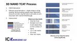
Figure 1 illustrates the 3D NAND TCAT Process.
Figure 1. 3D NAND TCAT Process.
In the 3D NAND segment, the market leader is Samsung and they use the TCAT process illustrated in this slide. Number two in the market is Kioxia (formerly Toshiba Memory) and they use an essentially identical process. Micron Technology is also adopting a charge trap process we expect to be similar to this process making this process representative of the majority of the industry. SK Hynix uses a different process that still shares many key elements with this process. The only companies not using a charge-trap process are Intel-Micron and now that Intel and Micron have split apart on 3D NAND, Intel will be the only company pursuing floating gate.
The basic process has three major sections:
- Fabricate the CMOS – the CMOS writes, reads and erases the bits. Initially everyone except Intel-Micron fabricated the CMOS next to the memory array with Intel-Micron fabricating some of the CMOS under the memory array. Over time other companies have migrated to CMOS under the array and we expect within a few generations that all companies will migrate to CMOS under the array because it offers better die area utilization.
- Fabricate the memory array – for charge trap the array fabrication takes place by depositing alternating layers of oxide and nitride. A channel hole is then etched down through the layers and refilled with an oxide-nitride-oxide (ONO) layer, a poly silicon tube (channel) and filled with oxide. A stair step is then fabricated using a mask – etch – mask shrink – etch approach. A slot is then etched down through the array and the nitride film is etched out. Blocking films and tungsten are then deposited to fill the horizontal openings where the nitride was etched out. Finally, vias are etched down to the horizontal sheets of tungsten.
- Interconnect – the CMOS and memory array are then interconnected. For CMOS under the array, some interconnect takes place before the memory array fabrication.
This approach is very mask efficient because many layers can be patterned with a few masks. The overall process requires a channel mask, several stair steps masks depending on the number of layers and process generation, in early generation processes, a single mask could produce approximately 8-layers but some process today can reach 32-layers with a single mask. The slot requires a mask, sometimes there is also a second shallow slot that requires a mask and finally via requires a mask.
The channel hole etching is a very difficult high-aspect-ratio (HAR) etch and once a certain maximum number of layers is reached the process must be broken up into “strings” in something called “string stacking”. In string stacking, basically, a set of layers is deposited, a mask is applied, and the channel is etched and filled. Then another set of layers is deposited and masked, etched and filled. In theory this can be done many times. Intel-Micron use a floating gate process that uses oxide-polysilicon layers that are much more difficult to etch than oxide-nitride layers, and they were the first to string stack. Figure 2 illustrates Intel-Micron string stacking.
Figure 2. Intel-Micron String Stacking.
Each company has their own approach to channel etching and their own limit in terms of when they string stack. Because they use oxide-poly layers Intel-Micron produced a 64-layer device by stacking 2 – 32-layer strings and then produced a 96-layer device by stacking 2 – 48-layer strings. Intel has announced a 144-layer device that we expect to be 3 – 48-layer strings. SK Hynix began string stacking at 72-layers and Kioxia at 96-layers (both charge trap processes with alternating oxide-nitride layers). Samsung is the last holdout on string stacking having produced a 92-layer device as a single string and they have announced a 128-layer – single string device.
Memory density can also be improved by storing multiple bits in a cell. NAND Flash has moved through a progression from 1 bit – single-level cell (SLC), to 2 bit – multi-level cell (MLC), to 3 bit – three-level cell (TLC), to 4 bit – quadruple-level cell (QLC). Companies are now preparing to introduce 5 bit – penta-level cells (PLC) and there is even discussion of 6 bit – hexa-level cells (HLC). Increasing the number of bits per cell helps with density but the benefit is decreasing, SLC to MLC is 2.00 the bits, MLC to TLC is 1.50x the bits, TLC to QLC is 1.33x the bits, QLC to PLC will be 1.25x the bits and if we get there PLC to HLC will be 1.20x the bits.
Figure 3 presents string stacking by year and company on the left axis and maximum bits per cell on the right axis.
Figure 3. Layers, Stacking and Bits per Cell.
Figure 4 presents our analysis of the resulting mask counts by exposure type, company and year. The dotted line is the average masks by year that is increasing from 42 in 2017 to 73 in 2025, this contrasts with the layers increasing from an average of 60 in 2017 to 512 in 2025. In other words, only a 1.7x increase in masks is required to produce an 8.5x increase in layers highlighting the mask efficiency of the 3D NAND processes.
Figure 4. Mask Count Trend.
Figure 5 presents actual and forecast bit density by company and year for both 2D NAND and 3D NAND. This is the bit density for the whole die or in other words the die bit capacity divided by the die size.
Figure 5. NAND Bit Density.
From 2000 to 2010, 2D NAND bit densities were increasing by 1.78x per year driven by lithographic shrinks. Around 2010 the difficulty of continuing to shrink 2D NAND led to a slow down to 1.43x per year until around 2015 when 3D NAND became the driver and continued at a 1.43x per year rate. We are projecting a slight slowdown from 2020 to 2025 to 1.38x per year. This is an improvement in our forecast from last year because we are seeing the companies push the technology faster than we originally expected. Finally, SK Hynix has talked about 500 layers in 2025 and 800 layers in 2030 resulting in a further slow down after 2025.
Figure 6 presents NAND Bit Cost Trends.
Figure 6. NAND Bit Cost Density.
In this figure we have taken wafer costs calculated using our Strategic Cost and Price Model and combined them with the bit density from figure 5 to produce a bit cost trend. In all cases the fabs are new greenfield 75,000 wafer per month fabs because that is the average capacity of NAND fabs in 2020. The countries where the fabs are located are Singapore for Intel-Micron, China for Intel, Japan for Kioxia and South Korea for Samsung and SK Hynix. These calculations do not include packaging and test costs, do not take into street width and have only rough die yield assumptions in them.
The first three nodes on the chart are 2D NAND where we see a 0.7x per node cost trend. With the transition to 3D NAND the bit cost initially increased for most companies but has now come down below 2D NAND bits costs and is following a 0.7x per node trend until around 300 to 400 layers. At 300-400 layers we project the cost per but will level out possibly placing an economic limit on this technology unless there are some breakthroughs in process or equipment efficiency.
Logic
For 3D NAND “nodes” are easy to define based on physical layers, for DRAM nodes are the active half-pitch, for logic nodes are pretty much whatever the marketing guys at a company wants to call them.
Some people consider the current leading edge FinFET processes to be 3D because the FinFET is a 3D structure but in the context of this discussion we consider 3D to be when device stacking allows multiple active layers to be stacked up to create stacks of devices. In this context 3D Logic will really come in once CFETs are adopted.
Figure 7 presents the nodes by year for the 3 companies pursuing the state of the art.
Figure 7. Logic Roadmap.
The node comparisons in this chart are complicated by the split between Intel and the foundries. Intel has followed the classic node names, 45nm, 32nm, 22nm, 14nm whereas the foundries have followed the “new” node names of 40nm, 28nm, 20nm, 14nm. Furthermore, intel has shrunk more per node and so Intel 14nm has similar density to foundry 10nm and Intel 10nm has similar density to foundry 7nm.
At the top of the figure I have outlined a consistent node name series based on alternating 0.71 and 0.70 shrinks.
In the bottom of the figure I have nodes by company and year with transistor density for each node. The transistor density is calculated based on a weighting of NAND and Flipflop cells as I have previously discussed. Next to each node in parenthesis is either FF for FinFET, HNS for horizontal nanosheet, HNS/FS for horizontal nanosheets with a dielectric wall (Forksheet) to improve density based on work Imec has done and CFET for complimentary stacked FETs where nFETs and pFETs are vertically stacked. CFETs will be when logic crosses over into a layer-based scaling approach and becomes a true 3D solution, in principle CFETs can continue to scale by adding more layers.
Bold indicates leading density or technology. In 2014 Intel takes the density lead with their 14nm process. In 2016 TSMC takes the density lead with their 10nm process and maintains the lead in 2017 with their 7nm process. TSMC and Samsung have similar densities at 7nm but going to 5nm TSMC is producing a much larger shrink than Samsung and in 2019 TSMC maintains the process density lead with their 5nm technology. If Samsung delivers on their HNS technology in 2020 that we are calling a 3.5nm node, they may take the density lead and be the first company to manufacture HNS. In 2021 the TSMC node we are calling 3.5nm may return them to the density lead. If Intel can deliver on their two-year cadence with the kind of shrinks they typically target we believe they could take the density lead in 2023 with their 5nm process. In 2024 we may see a first CFET implementation from Samsung taking the density lead until 2025 when Intel may regain the lead with their first CFET process.
Figure 8 presents the logic mask counts for these processes. The introduction of EUV is mitigating mask layers, without EUV we would likely see over 100 masks on this chart. As we did with the NAND mask count figure, the dotted line is average mask counts. We have also grouped processes based on “similar” densities so for example Intel 14nm is combined with the foundry 10nm process and intel 10nm with the foundry 7nm processes.
Figure 8 Logic Mask Counts.
Figure 9 presents the logic density in transistors per millimeter squared based on the NAND/Flipflop weighting metric mentioned previously.
Figure 9. Logic Density Trend.
There are six types of processes plotted on this chart.
Planar transistors were the primary leading-edge logic process until around 2014 and produced a density improvement of 1.33x per year, FinFETs then took over at the leading edge and have provided a 1.29x per year density improvement. In parallel to FinFETs we have seen the introduction of FDSOI processes. FDSOI offers simpler processes with lower design costs and better analog, RF and power but cannot compete with FinFETs for density or raw performance. When HNS takes over from FinFETs we expect the rate of density improvement to further slow to 1.16x per year and eventually CFETs take over and increase density at 1.11x per year. We have also plotted SRAMs produced by vertical transistors based on work by Imec that may provide an efficient solution for cache memory chiplets.
Figure 10 illustrates the trend in logic transistor cost.
Figure 10. Logic Transistor Cost.
Figure 10 presents the cost per billion transistors by combining wafer cost estimates from our Strategic Cost and Price Model with the transistor densities in figure 9. All fabs are assumed to be new greenfield fabs with 35,000 wafers per month capacity because that is the average size of logic fabs in 2020. The assumed countries are Germany for GLOBALFOUNDRIES except for 14nm that is done in the United States, the United States is also assumed for Intel except for 10nm in Israel, South Korea is assumed for Samsung and Taiwan for TSMC.
This plot does not include mask set or design cost amortization so while manufacturing cost per transistor is coming down the number of designs that can afford to access these technologies is limited to high volume products.
This plot does not include any packaging, test or yield impact.
From 130nm down to the i32/f28 (intel 32nm/foundry 28nm) node costs were coming down by 0.6x per node, then at the i22/f20 and f16/f14 node the cost reductions slowed because the foundries decided not to scale for their first FinFET processes. This slow down led to many in the industry erroneously predicting the end of cost reduction. From the f16/f14 node down to the i5/f2.5 node we expect costs to decrease by 0.72x per node and then slow to 0.87x per node thereafter. The g1.25 and g0.9 nodes are generic CFET processes with 3 and 4 decks respectively.
Figure 11 examines the impact of mask set amortization on wafer cost.
Figure 11. Mask Set Amortization.
The wafer costs in figure 11 are based on a new greenfield fab in Taiwan running 40,000 wafers per month. The amortization is mask set only and does not include design costs.
The table presents the 2020 mask set cost for 250nm, 90nm, 28nm and 7nm mask sets. Please note that at introduction these mask sets were more expensive. The mask set cost is them amortized over a set number of wafers and the resulting normalized costs are shown in the figure. In the table the wafer cost ratio is the wafer cost with amortization for 100 wafers run on a mask set divided by the wafer cost with amortization for 100,000 wafers run on a mask set.
From the figure and table, we can see that mask set amortization has a small effect at 250nm (1.42x ratio) and a large effect at 7nm (18.05x ratio). Design cost amortization is even worse.
The bottom line is that design and mask set costs are so high at the leading edge that only high-volume products can absorb the resulting amortization.
DRAM
Leading edge DRAMs have capacitor structures that are high aspect ratio “3D” devices but similar to current logic devices, DRAM doesn’t have scaling by stacking of active elements.
Figure 12 presents DRAM nodes by company in the top table and on the bottom of the figure are some of the key structures.
Figure 12. DRAM Nodes.
As DRAM nodes proceeded below the 4x nm generation the buried saddle fin access transistor with buried word line came into use (see bottom left). The bottom right illustrates the progression of the capacitor structure to higher aspect ratio structures with two layers of silicon nitride “MESH” support. DRAM capacitor structures are reaching the mechanical stability limits of the technology and with dielectric k values also stalled, DRAM scaling is evolving into single nanometer per node scaling.
Figure 13 illustrates mask counts by exposure type and company.
Figure 13. DRAM Mask Counts.
From figure 13 it can be seen that from the 2x to 2y generation there is a big jump in mask counts. The jump is driven by performance and power requirements that led to the need for more transistor types and threshold voltages in the peripheral logic.
At the 1x node Samsung is the first company to introduce EUV to DRAM production and the number of EUV layers grows at the 1a, 1b and 1c nodes. SK Hynix is also expected to implement EUV, we do not currently expect Micron to implement EUV.
Figure 14 illustrates the trend in DRAM bit density by year.
Figure 14. DRAM Bit Density.
In figure 14 the bit density is the product capacity in gigabytes divided by the die size in millimeters square.
Form figure 14 is can be seen that there has been a slowdown in bit density growth beginning around 2105. DRAM bit density is currently constrained by the capacitor and it isn’t clear what the solution will be. Long term a new type of memory may be needed to replace DRAM. DRAM requires relatively fast access with high endurance and currently MRAM and FeRAM appear to be the only options that have the potential to meet the speed and endurance requirements. Because MRAM requires relatively high current to switch, large selector transistors are required constraining the ability to shrink MRAM to competitive density and cost. FeRAM is also a potential replacement and is getting a lot of attention at places like Imec.
Figure 15 illustrates the DRAM bit cost trend.
Figure 15. DRAM Bit Cost Trend.
Figure 15 is based on combining wafer cost estimates from our Strategic Cost and Price Model with the bit densities in figure 14. All fabs are assumed to be new greenfield fabs with 75,000 wafers per month capacity because that is the average size of DRAM fabs in 2020. The assumed countries are Japan for Micron and South Korea for Samsung and SK Hynix.
These calculations do not include packaging and test costs and do not take into street width or die yield.
In this plot the combination of higher mask counts and slower bit density growth lead to a slow down from 0.70x per node cost trend to a 0.87x per node cost trend.
Conclusion
NAND has successfully transitioned from 2D to 3D and now has a scaling path until around 2025. After 2025 scaling may be possible with very high layers counts but unless a breakthrough in the process or equipment efficiency is made, cost per bit reductions may end.
Leading edge logic today utilizes 3D FinFET structures but won’t be a true stacked device 3D technology until CFETs are introduced around 2025. Logic has the potential to continue to scale until the end of the 2020s by transitioning from FinFET to HNS to CFET although the cost improvements will likely slow down.
DRAM is the most constrained of the 3 market segments, scaling and cost reductions have already slowed down significantly and no solution is currently known. Slower bit density and cost scaling will likely continue until around 2025 when a new memory type may be needed.
Here is the full presentation:
Lithovision 2020
Also Read:
IEDM 2019 – Imec Interviews
IEDM 2019 – IBM and Leti
The Lost Opportunity for 450mm